JP2007298950A - Method and apparatus for reducing irregularity in color filter - Google Patents
Method and apparatus for reducing irregularity in color filter Download PDFInfo
- Publication number
- JP2007298950A JP2007298950A JP2007026439A JP2007026439A JP2007298950A JP 2007298950 A JP2007298950 A JP 2007298950A JP 2007026439 A JP2007026439 A JP 2007026439A JP 2007026439 A JP2007026439 A JP 2007026439A JP 2007298950 A JP2007298950 A JP 2007298950A
- Authority
- JP
- Japan
- Prior art keywords
- ink droplets
- ink
- size
- lateral position
- relative lateral
- Prior art date
- Legal status (The legal status is an assumption and is not a legal conclusion. Google has not performed a legal analysis and makes no representation as to the accuracy of the status listed.)
- Pending
Links
Images


Classifications
-
- G—PHYSICS
- G02—OPTICS
- G02B—OPTICAL ELEMENTS, SYSTEMS OR APPARATUS
- G02B5/00—Optical elements other than lenses
- G02B5/20—Filters
- G02B5/201—Filters in the form of arrays
-
- B—PERFORMING OPERATIONS; TRANSPORTING
- B41—PRINTING; LINING MACHINES; TYPEWRITERS; STAMPS
- B41J—TYPEWRITERS; SELECTIVE PRINTING MECHANISMS, i.e. MECHANISMS PRINTING OTHERWISE THAN FROM A FORME; CORRECTION OF TYPOGRAPHICAL ERRORS
- B41J2/00—Typewriters or selective printing mechanisms characterised by the printing or marking process for which they are designed
- B41J2/005—Typewriters or selective printing mechanisms characterised by the printing or marking process for which they are designed characterised by bringing liquid or particles selectively into contact with a printing material
- B41J2/01—Ink jet
- B41J2/07—Ink jet characterised by jet control
-
- B—PERFORMING OPERATIONS; TRANSPORTING
- B41—PRINTING; LINING MACHINES; TYPEWRITERS; STAMPS
- B41J—TYPEWRITERS; SELECTIVE PRINTING MECHANISMS, i.e. MECHANISMS PRINTING OTHERWISE THAN FROM A FORME; CORRECTION OF TYPOGRAPHICAL ERRORS
- B41J2/00—Typewriters or selective printing mechanisms characterised by the printing or marking process for which they are designed
- B41J2/005—Typewriters or selective printing mechanisms characterised by the printing or marking process for which they are designed characterised by bringing liquid or particles selectively into contact with a printing material
- B41J2/01—Ink jet
-
- G—PHYSICS
- G02—OPTICS
- G02B—OPTICAL ELEMENTS, SYSTEMS OR APPARATUS
- G02B5/00—Optical elements other than lenses
- G02B5/20—Filters
- G02B5/22—Absorbing filters
- G02B5/223—Absorbing filters containing organic substances, e.g. dyes, inks or pigments
-
- G—PHYSICS
- G02—OPTICS
- G02F—OPTICAL DEVICES OR ARRANGEMENTS FOR THE CONTROL OF LIGHT BY MODIFICATION OF THE OPTICAL PROPERTIES OF THE MEDIA OF THE ELEMENTS INVOLVED THEREIN; NON-LINEAR OPTICS; FREQUENCY-CHANGING OF LIGHT; OPTICAL LOGIC ELEMENTS; OPTICAL ANALOGUE/DIGITAL CONVERTERS
- G02F1/00—Devices or arrangements for the control of the intensity, colour, phase, polarisation or direction of light arriving from an independent light source, e.g. switching, gating or modulating; Non-linear optics
- G02F1/01—Devices or arrangements for the control of the intensity, colour, phase, polarisation or direction of light arriving from an independent light source, e.g. switching, gating or modulating; Non-linear optics for the control of the intensity, phase, polarisation or colour
- G02F1/13—Devices or arrangements for the control of the intensity, colour, phase, polarisation or direction of light arriving from an independent light source, e.g. switching, gating or modulating; Non-linear optics for the control of the intensity, phase, polarisation or colour based on liquid crystals, e.g. single liquid crystal display cells
- G02F1/133—Constructional arrangements; Operation of liquid crystal cells; Circuit arrangements
- G02F1/1333—Constructional arrangements; Manufacturing methods
- G02F1/1335—Structural association of cells with optical devices, e.g. polarisers or reflectors
- G02F1/133509—Filters, e.g. light shielding masks
- G02F1/133514—Colour filters
- G02F1/133516—Methods for their manufacture, e.g. printing, electro-deposition or photolithography
Abstract
Description
本出願は、2006年2月7日に、「カラーフィルタにおける不整を低減するための方法及び装置」の名称で出願された米国特許仮出願第60/771284号に基づく優先権を主張し、この出願は引用により全ての目的のため全体的に本願に組み込まれる。 This application claims priority from US Provisional Application No. 60/771284 filed on Feb. 7, 2006 under the title "Method and Apparatus for Reducing Irregularities in Color Filters" The application is incorporated herein by reference in its entirety for all purposes.
本出願は以下の共通して譲渡され、同時に係属中の出願に関連し、これらの出願は引用により全ての目的のため全体的に本願に組み込まれる。
2005年2月18日に「印字ヘッドアセンブリを精密制御するための方法及び装置」の名称で出願された米国特許出願第11/061120号(代理人整理番号9769)。
2005年9月29日に「ディスプレイ用インクジェット印刷カラーフィルタのための方法及び装置」の名称で出願された米国特許出願第11/238632号(代理人事件整理番号9521−5/P01)。
This application is related to the following commonly assigned and concurrently pending applications, which are incorporated herein by reference in their entirety for all purposes.
US patent application Ser. No. 11/061120 (Attorney Docket No. 9769) filed on Feb. 18, 2005 under the title “Method and Apparatus for Fine Control of Printhead Assembly”.
U.S. Patent Application No. 11/386632 (Attorney Docket No. 9521-5 / P01) filed on September 29, 2005, under the name "Method and Apparatus for Inkjet Printing Color Filters for Display".
本発明は一般に電子機器製造方法に係り、特にはフラットパネルディスプレイ用カラーフィルタの製造に関する。 The present invention generally relates to an electronic device manufacturing method, and more particularly to manufacturing a color filter for a flat panel display.
フラットパネルディスプレイ産業は、ディスプレイ装置、特にカラーフィルタを製造するためにインクジェット印刷を用いようと試みてきた。インクジェット印刷を効果的に用いる際の1つの問題点は、高いスループットを保ちながら正確かつ精密に基板上にインク又はその他の材料をインクジェットすることが困難であるということである。従って、インクジェットヘッドを用いて基板上に効率的に印刷するための改善された方法及び装置が必要とされる。 The flat panel display industry has attempted to use inkjet printing to manufacture display devices, particularly color filters. One problem with using inkjet printing effectively is that it is difficult to inkjet ink or other materials onto a substrate accurately and precisely while maintaining high throughput. Accordingly, there is a need for an improved method and apparatus for efficiently printing on a substrate using an inkjet head.
本発明の一態様において、インク液滴を基板上でピクセルウェル内に堆積し、それに続いて同じピクセルウェル内に堆積させるインク液滴のサイズを意図的に変える方法を提供する。変更サイズをランダムに選択し、ムラ不整の発生を防止する。 In one aspect of the invention, a method is provided for intentionally changing the size of an ink droplet that is deposited in a pixel well on a substrate and subsequently deposited in the same pixel well. The change size is selected at random to prevent unevenness.
本発明の他の態様において、インク液滴を基板上でピクセルウェル内に堆積し、それに続いて同じピクセルウェル内に堆積させる液滴の相対位置を意図的に変える方法を提供する。変更位置をランダムに選択し、ムラ不整の発生を防止する。 In another aspect of the present invention, a method is provided for intentionally altering the relative position of droplets that are deposited in a pixel well on a substrate and subsequently deposited in the same pixel well. The change position is randomly selected to prevent unevenness.
更に、本発明の他の態様において、複数のインク液滴を基板上でピクセルウェル列に堆積し、ピクセルウェルに堆積させるインク液滴のサイズを意図的に変えることを含む方法を提供する。 Furthermore, in another aspect of the invention, a method is provided that includes depositing a plurality of ink droplets in a pixel well row on a substrate and deliberately changing the size of the ink droplets deposited in the pixel wells.
更に、本発明の他の態様において、複数のインク液滴を基板上でピクセルウェル列に堆積するよう構成した印字ヘッドと、印字ヘッドによってピクセルウェルに堆積させるインク液滴のサイズを変えられるよう構成した制御装置とを含む装置を提供する。 Furthermore, in another aspect of the present invention, a print head configured to deposit a plurality of ink droplets on a pixel well array on a substrate, and a size of the ink droplets deposited on the pixel wells by the print head can be changed. And a control device.
更に、本発明の他の態様において、複数のインク液滴を基板上でピクセルウェル列に堆積し、ピクセルウェルに堆積させるインク液滴の相対横位置を意図的に変えることを含む方法を提供する。 Further, in another aspect of the present invention, a method is provided that includes depositing a plurality of ink droplets in a pixel well row on a substrate and deliberately changing the relative lateral position of the ink droplets deposited in the pixel wells. .
更に、本発明の他の態様において、複数のインク液滴を基板上でピクセルウェル列に堆積するよう構成した印字ヘッドと、印字ヘッドによってピクセルウェルに堆積させるインク液滴の相対横位置を変えられるよう構成した制御装置とを含む装置を提供する。 Furthermore, in another aspect of the present invention, a print head configured to deposit a plurality of ink droplets on a pixel well array on a substrate, and a relative lateral position of the ink droplets deposited on the pixel wells by the print head can be changed. And a control device configured as described above.
本発明のその他の構成及び態様は、典型的な実施形態についての以下の詳細な説明、特許請求の範囲及び添付図面からより充分に明らかになる。 Other features and aspects of the present invention will become more fully apparent from the following detailed description of the exemplary embodiments, the appended claims and the accompanying drawings.
本発明は、フラットパネルディスプレイ用のカラーフィルタの製造で起こる誤差状態を排除するためのシステム及び方法を提供する。誤差状態は、インクジェットプリンタを使用して精密にインク、あるいは別の材料を基板上に堆積してカラーフィルタを形成する際に起こり得る現象に起因する。精度における機械的、電気的な限界により、基板上に噴射されたインク液滴の容量及び位置は理想の目標サイズ及び/又は位置から一様にずれ、インクを堆積しているプリンタが例え公差内で作動しているとしても、各液滴について同じ小さな誤差を繰り返すことによる蓄積効果は、インクジェットプリンタを用いて製造したカラーフィルタを備えたフラットパネルディスプレイを裸眼で見ても見える不整となって現れる。即ち、1つ1つの液滴の理想位置からのズレが目に見えないものだけとなるようインク液滴を公差内で安定的に堆積させたとしても、このように均一に配置された一連の液滴が全体としては目に見えるムラとなる場合がある。この誤差は、ムラ不整又はムラ効果と呼ぶことができる。ムラとは、日本語を音訳したものであり、明らかに対応する英単語を有さない。 The present invention provides a system and method for eliminating error conditions that occur in the manufacture of color filters for flat panel displays. The error condition results from a phenomenon that can occur when an ink jet printer is used to precisely deposit ink or another material on a substrate to form a color filter. Due to mechanical and electrical limitations in accuracy, the volume and position of the ink droplets ejected onto the substrate will deviate uniformly from the ideal target size and / or position, and the printer depositing the ink will be within tolerances. Even if it is operating on, the accumulation effect of repeating the same small error for each droplet appears as an irregularity that can be seen with the naked eye on a flat panel display with a color filter manufactured using an inkjet printer . That is, even if the ink droplets are stably deposited within the tolerance so that the deviation from the ideal position of each droplet is not visible, a series of uniformly arranged in this way In some cases, the droplets may become visible unevenness as a whole. This error can be referred to as unevenness or unevenness effect. Unevenness is transliteration of Japanese and clearly has no corresponding English word.
本発明は、フラットパネルディスプレイにムラ不整を起こすことなくカラーフィルタを印刷するための方法及び装置を提供する。本発明により、基板上にインク液滴を堆積する際に起こる量のばらつきは意図的に増大させられ(例えば、プリンタの最高精度によって規定される最小変動量から)、隣接するピクセル又はピクセルの集合における、液滴位置及び/又はサイズにおける目に見える画一的繰り返しが回避される。 The present invention provides a method and apparatus for printing color filters without causing irregularities in flat panel displays. With the present invention, the amount of variation that occurs when depositing ink droplets on a substrate is intentionally increased (eg, from the minimum amount of variation defined by the highest accuracy of the printer) and adjacent pixels or collections of pixels. Visible uniform repeats in droplet position and / or size are avoided.
図1は、理想的なカラーフィルタ100の一例の拡大したものである。カラーフィルタ100はブラックマトリクス材料104によって画成されたピクセル列を備えた基板102を含む。各ピクセル106は、各々が一連のインク液滴110で満たされた三色(例えば、赤、緑、青)のサブピクセルウェル108を含む。図示した例においては、各サブピクセルウェル108には4滴のインク110が一列に堆積されている。製造中、基板102はXYテーブルによって駆動され、印字ヘッド(図示せず)の下のステージ上に移動される。印字ヘッドは、4滴のインクを各サブピクセルウェル108に堆積した。
FIG. 1 is an enlarged view of an example of an
図1のカラーフィルタ100は理想的なカラーフィルタの平面図を表したものであり、各サブピクセル108は、各サブピクセルウェル108のちょうど中心に列状に堆積された、同一サイズの液滴110を含む。インク液滴の理想的なサイズ決め及び配置の達成は困難である。個々の印字ヘッドノズルを始動しインクを噴射させるために使用される信号間の電気的クロストークを含む様々な要因が、液滴サイズにおけるばらつきを生み出す。中でも、XYテーブル(ステージ)はもとより印字ヘッドノズルの整列における機械的誤差は、位置決めにおける誤差につながる可能性がある。こういった類の誤差はかなりの範囲までは修正し得るが、例えば、各ノズルの発信パルス電圧信号(液滴サイズを制御する)を調節して閾値パーセンテージ誤差公差未満になるよう、又は液滴着地精度が±閾値距離未満にまで改善されるようにすることは困難及び/又は非常にコストがかかる。例えば、アプライドマテリアル社製の現在の世代のインクジェットプリンタは、発信パルス電圧を1%公差にまで制御することができ、これは±10%の容量誤差と±5μmまでの液滴着地精度になる。これらの精度閾値又は公差は目的のピクセルウェル内に適切なサイズの液滴を常に着地させるものの、これらの公差はムラ不整の発生を回避するに充分なものではない場合がある。
The
図2を参照すると、カラーフィルタ200の平面図の一例を拡大したものが描かれており、矢印はムラ不整202を示す。液滴100は全て各自のピクセルウェル106に適合するよう位置決め、サイズ合わせがされている、つまり公差内にあることに留意する必要がある。公差内にあるにも関わらずムラ不整は起こる場合があり、例えば、サブピクセル列における液滴の一部が各々のサブピクセルウェルの中心から若干ずれて配置される。図3は濃淡のない白い視野を示す一方ムラ不整302を示すフラットパネルディスプレイ300の出力の一例を描いたものである。ムラ不整が存在するとき、線が目に見えることに留意する必要がある。
Referring to FIG. 2, an enlarged plan view of an example of the
図4は、各々3つのサブピクセルを有する二列のピクセルの斜視図である。各サブピクセルの高さが、サブピクセルに堆積されたインクの総量を示す。矢印がムラ不整を示す場所において、隣接するサブピクセル列は2列のインク量間に一貫して比較的大きな差を有することに留意する必要がある。この効果は、公称インク量の列に隣接する列に堆積されるインクの量が一様に低下及び/又は増加することから起こる。この問題は、インク量が増加した列に隣接する列のインク量が低下することにより悪化する場合がある。従って、図2の例に示される一様に中心からズレたインク液滴又は図4に示されるインク量の一様な低下(又は増加)は、図3に示される目に見えるムラ効果につながる可能性がある。更に、一貫して中心からズレた液滴と、一貫して量が低下又は増加したインクが組み合わさることにより、たとえその片方だけでは目に見えるムラ効果は起こらないとしても、累積したムラ効果が生じる場合がある。 FIG. 4 is a perspective view of two rows of pixels each having three subpixels. The height of each subpixel indicates the total amount of ink deposited on the subpixel. It should be noted that where the arrows indicate unevenness, adjacent subpixel columns have consistently relatively large differences between the two ink amounts. This effect arises from the uniform decrease and / or increase in the amount of ink deposited in a row adjacent to the nominal ink amount row. This problem may be exacerbated by a decrease in the ink amount in a row adjacent to the row in which the ink amount has increased. Accordingly, the ink droplet uniformly displaced from the center shown in the example of FIG. 2 or the uniform drop (or increase) of the ink amount shown in FIG. 4 leads to the visible unevenness effect shown in FIG. there is a possibility. In addition, the combination of consistently misaligned droplets and consistently reduced or increased amounts of ink results in a cumulative mura effect, even if only one of them does not cause a visible mura effect. May occur.
感覚的には逆だが、本発明は、インクジェットプリンタの公称誤差公差を上げることによりムラ不整問題を解決する。つまり、プリンタの設定作動閾値がなんであれ、その値より低く誤差公差を低減しようと試みるのではなく、本発明は目的液滴サイズ及び/又は液滴位置を変化させて、そのままでは目に見えるムラ不整となる一連の液滴における同じ微誤差を防ぐ。図5は、各々3つのサブピクセルを備えた2列のピクセルの斜視図である。図4と同様に、各サブピクセルの高さは各々のサブピクセルに堆積されたインクの総量を表す。異なるサブピクセル間におけるインク量のばらつきが増大しており、ゆえに、どの列においても一定してインク量が少ない(又は多い)ということがないことに留意する必要がある。従って、液滴サイズにおけるこのばらつきは、液滴サイズ及び/又は液滴位置に関連して起こる目に見えるムラ効果を回避するのに使用することができる。 Although sensibly the reverse, the present invention solves the unevenness problem by increasing the nominal error tolerance of an inkjet printer. In other words, whatever the set operating threshold of the printer is, the present invention does not attempt to reduce the error tolerance lower than that value, but the present invention changes the target droplet size and / or the droplet position to make the visible unevenness as it is. Prevents the same minor error in a series of irregular droplets. FIG. 5 is a perspective view of two rows of pixels, each with three subpixels. Similar to FIG. 4, the height of each subpixel represents the total amount of ink deposited on each subpixel. It should be noted that the variation in ink amount between different sub-pixels is increasing, and therefore there is no consistently low (or high) ink amount in any column. Thus, this variation in drop size can be used to avoid visible mura effects that occur in relation to drop size and / or drop position.
図6A、6B、7A、7Bは、図4、図5の例を各々作成するのに使用した実際値を示す表である。集計表600、700は、図4、図5の各々でプロットした総インク量を含む。これらの値は、原表602、604、702、704に記載のランダム生成液滴サイズデータ例を用いて計算された。この例において、各ピクセル(サブピクセル)は表602、604、702、704で1、2、3、4と番号をふられ、液滴サイズで表されている4滴のインクを充填されている。ピクセル識別符号(例えば、aR1、aG1、aB1等)の下に並ぶ値は、各々のサブピクセルに堆積された4滴の液滴サイズの合計(例えば、総量)である。総量値は、集計表600、700の各々の位置に入力される。 6A, 6B, 7A, and 7B are tables showing actual values used to create the examples of FIGS. 4 and 5, respectively. The tabulation tables 600 and 700 include the total ink amount plotted in each of FIGS. These values were calculated using the randomly generated droplet size data examples described in the original tables 602, 604, 702, 704. In this example, each pixel (sub-pixel) is numbered 1, 2, 3, 4 in Tables 602, 604, 702, 704 and is filled with 4 drops of ink represented by drop size. . The values listed below the pixel identification code (for example, aR1, aG1, aB1, etc.) are the total (for example, the total amount) of the droplet sizes of the four droplets deposited on each subpixel. The total amount value is input to each position of the summary tables 600 and 700.
生成した際、図6A及び6Bのランダム液滴サイズデータ例は理想/目標値の±10パーセント以内に抑制された。よって、目標値が25plの場合、個々の液滴サイズは22.5plから27.5plにわたるが、任意のサブピクセル列内における液滴サイズは一定である。この一貫性は、任意のサブピクセル列にインクを堆積するのに同一の印字ヘッドノズルが使用され、誤差が同一サイズの液滴から液滴へと同じまま残るからである。対照的に、図7A、7Bのランダム生成液滴サイズデータ例は、任意のサブピクセル列(例えば、任意の印字ヘッドノズル)について±10パーセントで変化しており、容量誤差は±10%であった。これにより、総公称誤差が±20%、個々の液滴は20plから30plとなるが、これらは任意のサブピクセル列内で異なる。同一液滴サイズを繰り返す場合とは異なり、液滴サイズが異なると、誤差の幅は異なるサイズの液滴ごとに変わり得ることに留意する必要がある。これらの値と範囲は単に例として挙げたに過ぎず、多くの異なる値と範囲が使用可能であることに留意する必要がある。液滴サイズ及び位置を変化させるための様々な方法が、引用よって以前に本願に組み込まれた文献に詳細に記載されている。 When generated, the random droplet size data example of FIGS. 6A and 6B was suppressed to within ± 10 percent of the ideal / target value. Thus, when the target value is 25 pl, the individual droplet size ranges from 22.5 pl to 27.5 pl, but the droplet size in any subpixel column is constant. This consistency is because the same printhead nozzle is used to deposit ink on any subpixel column, and the error remains the same from drop to drop of the same size. In contrast, the example randomly generated droplet size data in FIGS. 7A and 7B vary by ± 10 percent for any subpixel column (eg, any printhead nozzle) with a volume error of ± 10%. It was. This results in a total nominal error of ± 20% and individual drops from 20 pl to 30 pl, but these are different within any subpixel column. It should be noted that, unlike the case of repeating the same droplet size, the error width can vary for different size droplets for different droplet sizes. It should be noted that these values and ranges are merely given as examples, and many different values and ranges can be used. Various methods for changing the droplet size and position are described in detail in the literature previously incorporated herein by reference.
図6Aの集計表600と比較した図7Aの集計表700からわかるように、公称誤差を上げることにより、液滴サイズのばらつき度が増大する。集計表600、700のプロットからわかるように、図4及び5において、このばらつきは目に見えるムラ効果の発生を回避するために使用し得る。 As can be seen from the summary table 700 of FIG. 7A compared to the summary table 600 of FIG. 6A, increasing the nominal error increases the degree of variation in droplet size. As can be seen from the plots in the summary tables 600, 700, in FIGS. 4 and 5, this variation can be used to avoid the occurrence of visible mura effects.
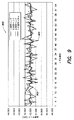
図8、図9は各々、本発明に従って液滴サイズにばらつきを導入することによりピクセルあたりのインク容量の標準偏差が低下することを示す表及びグラフである。図8の表800に示される例において、公称液滴サイズは直径42μmである。誤差は3.5%であり、よって、液滴サイズの範囲は41.265μmから42.735μmまで変動し得る。表800は、1つの印字ヘッドのノズルが平均して41.927μmの液滴(例えば16滴サブピクセル内に)を標準偏差0.432で列ごとに(例えば、プリントパスごとに)堆積することを表している。しかしながら、各ピクセルに堆積される16滴の液滴サイズを意図的に変えることにより、平均液滴サイズは42.009、標準偏差は0.092となり、これは1印字ヘッドでの結果の四分の一未満である。この結果は、ほぼ平坦な折れ線グラフ902(ノズル全体にわたる、意図的に変えた液滴サイズを示す)と、比較的急な山形の折れ線グラフ904(1つの印字ヘッドの液滴サイズを表す)とを比較させて図9にグラフ状に表されている。 8 and 9 are tables and graphs showing that the standard deviation of the ink capacity per pixel is lowered by introducing the variation in the droplet size according to the present invention. In the example shown in table 800 of FIG. 8, the nominal droplet size is 42 μm in diameter. The error is 3.5%, so the droplet size range can vary from 41.265 μm to 42.735 μm. Table 800 shows that one printhead nozzle averages 41.927 μm droplets (eg, in 16 droplet subpixels) to be deposited column by column (eg, every print pass) with a standard deviation of 0.432. Represents. However, by deliberately changing the size of the 16 drops deposited on each pixel, the average drop size is 42.09 with a standard deviation of 0.092, which is a quarter of the result with one printhead. Less than one. The result is a substantially flat line graph 902 (showing intentionally varied droplet sizes across the nozzles) and a relatively steep chevron line graph 904 (representing one printhead droplet size). Are shown in a graph in FIG.
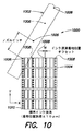
図10及び図11は、ムラ効果を回避するための付加的又は別の方法を示す。製造中のカラーフィルタ1000の拡大図が示されている。印字ヘッド1002は基板1004上方に位置した状態で示されており、基板1004をY軸指示によって示されるY方向で印字ヘッド1002下方に移動すると、印字ヘッド1002のノズル1006が整列してカラーフィルタ1000のサブピクセルウェル1008にインクが堆積される。各目標サブピクセルウェル1008内において、一連の液滴着地位置1010、1012は相互に繋いだ点によって表されている。
10 and 11 illustrate additional or alternative methods for avoiding the mura effect. An enlarged view of the
図10のカラーフィルタ1000は、プリンタの精度に照らし、インクをピクセルウェル1008の中心に可能な限り近接させて堆積する従来の方法を用いて製造されている。しかしながら、インク液滴着地位置オフセットMによって示されるように、サブピクセルウェル1008の一部の列における誤差(例えば、公差範囲内である±10μm)には目に見えるムラ効果につながるものもでることが予測される。
The
対照的に、図11のカラーフィルタ1000は、本発明の実施形態によって製造されている。インクを各サブピクセルの絶対横中心に直列に堆積しようとする代わりに、図11の液滴着地位置1012によって示されるように、ピクセルウェル1008にインク液滴を様々な横位置(例えば、固有の±10μm誤差に加えて±10μm)に堆積することを目標とする。
In contrast, the
一部の実施形態において、液滴サイズと同様に、液滴着地位置をランダムに、あるいは例えば図11に描かれる正弦曲線等の関数に基づいて変化させてもよい。液滴着地位置1012の変動は、印刷中に印字ヘッド位置を変化させること及び/又は印刷中に基板の位置を横方向に(例えば、印刷方向と直角に)移動させることによって達成してもよい。一部の実施形態において、印字ヘッド1002をステージ(基板を支持する台)又は基板位置の関数として、あるいは時間の関数として移動させてもよい。例えば、基板をステージによって印刷方向に移動させるにつれ、印字ヘッドをステージ位置に応じて、あるいは所定の周期、定数、変数に基づいて継続的に移動させる。例えば、フィルタ1000を印刷しながら(Y方向に向かって)、印字ヘッド1002をX方向に公称目標位置から±5から20μmで継続的に移動させる。印字ヘッド位置決め機構に連結された乱数発生器を用いて、所定の範囲内の±X方向移動変化量を継続的に選択してもよい。一部の実施形態においては、印字ヘッド1002の位置は、液滴ごとに(例えば、20KHz)、液滴群ごとに(例えば、〜800Hzから20KHz)、各ピクセルごとに(例えば、〜500から〜800Hz)、及び/又はピクセル群ごとに(例えば、各5から10ピクセル、50から60Hz)に変化させてもよい。インクジェットプリンタを用いた、液滴サイズと位置を変化させるための様々な方法は、参照することにより以前に本願に組み込んだ上述の文献に詳細に記載されている。一部の実施形態においては、サーボモータ又は圧電アクチュエータを用いて、印刷中に、印字ヘッド及び/又は基板/ステージの位置変化を正確に生じさせてもよい。別の実施形態においては、印字ヘッド1002を高周波及び/又は可変周波数で振動させて、位置変化を比較的ランダムに発生させてもよい。
In some embodiments, similar to the droplet size, the droplet landing position may be varied randomly or based on a function such as, for example, a sinusoid drawn in FIG. Variations in the
図12に示されるように、一部の実施形態において、本発明による液滴サイズ変化法及び位置変化法の双方を同時に用いてもよい。2つの方法を組み合わせることにより、ムラ効果の発生傾向を最低限に抑えるのに最適な液滴サイズ量及び/又は液滴位置変化量を見つけてもよい。 As shown in FIG. 12, in some embodiments, both the droplet size change method and the position change method according to the present invention may be used simultaneously. By combining the two methods, an optimal droplet size amount and / or droplet position change amount may be found to minimize the tendency of occurrence of the uneven effect.
上記説明は本発明の特定の実施形態のみを開示したものであり、上記で開示の方法及び装置を本発明の範囲内で改良したものは当業者には明らかである。例えば、いかなる種類のインク又はカラーフィルタ材料を用いてどの種類又はサイズのカラーフィルタの作成にも本発明は使用し得ることを当業者は理解し得る。従って、本発明はその特定の実施形態に関連して開示されたが、特許請求の範囲によって定義されるように、他の実施形態も本発明の精神と範囲に含まれることを理解しなくてはならない。 The foregoing description discloses only specific embodiments of the invention, and it will be apparent to those skilled in the art that the methods and apparatus disclosed above have been modified within the scope of the invention. For example, those skilled in the art can appreciate that the present invention can be used to make any type or size of color filter using any type of ink or color filter material. Thus, although the invention has been disclosed in connection with specific embodiments thereof, it should be understood that other embodiments are within the spirit and scope of the invention as defined by the claims. Must not.
Claims (38)
ピクセルウェルに堆積させるインク液滴のサイズを意図的に変化させることを含む方法。 Depositing multiple ink droplets onto a column of pixel wells on a substrate;
Intentionally changing the size of the ink droplets deposited in the pixel wells.
印字ヘッドによってピクセルウェルに堆積されるインク液滴のサイズを変化できるよう構成した制御装置とを含む装置。 A printhead configured to deposit a plurality of ink droplets onto a pixel well array on a substrate;
And a controller configured to change the size of the ink droplets deposited in the pixel wells by the print head.
ピクセルウェルに堆積させるインク液滴の相対横位置を意図的に変化させることを含む方法。 Depositing multiple ink droplets onto a pixel well array on a substrate;
A method comprising intentionally changing a relative lateral position of an ink droplet deposited on a pixel well.
印字ヘッドによってピクセルウェルに堆積されるインク液滴の相対横位置を変化できるよう構成した制御装置とを含む装置。 A printhead configured to deposit a plurality of ink droplets onto a pixel well array on a substrate;
And a controller configured to change the relative lateral position of the ink droplets deposited in the pixel well by the print head.
Applications Claiming Priority (1)
| Application Number | Priority Date | Filing Date | Title |
|---|---|---|---|
| US77128406P | 2006-02-07 | 2006-02-07 |
Publications (2)
| Publication Number | Publication Date |
|---|---|
| JP2007298950A true JP2007298950A (en) | 2007-11-15 |
| JP2007298950A5 JP2007298950A5 (en) | 2010-03-25 |
Family
ID=38600906
Family Applications (1)
| Application Number | Title | Priority Date | Filing Date |
|---|---|---|---|
| JP2007026439A Pending JP2007298950A (en) | 2006-02-07 | 2007-02-06 | Method and apparatus for reducing irregularity in color filter |
Country Status (5)
| Country | Link |
|---|---|
| US (1) | US7923057B2 (en) |
| JP (1) | JP2007298950A (en) |
| KR (2) | KR20070080580A (en) |
| CN (1) | CN101029943A (en) |
| TW (1) | TWI328520B (en) |
Cited By (3)
| Publication number | Priority date | Publication date | Assignee | Title |
|---|---|---|---|---|
| JP2008116929A (en) * | 2006-10-31 | 2008-05-22 | Icf Technology Ltd | Substrate structure having thin-film pattern layer and manufacturing method thereof |
| WO2010029957A1 (en) * | 2008-09-12 | 2010-03-18 | 株式会社アルバック | Ejection method and color filter manufacturing method |
| JP2019188387A (en) * | 2018-04-18 | 2019-10-31 | パナソニックIpマネジメント株式会社 | Printing method, printing device, el and solar battery manufacturing method |
Families Citing this family (11)
| Publication number | Priority date | Publication date | Assignee | Title |
|---|---|---|---|---|
| US7625063B2 (en) * | 2004-11-04 | 2009-12-01 | Applied Materials, Inc. | Apparatus and methods for an inkjet head support having an inkjet head capable of independent lateral movement |
| TWI312540B (en) * | 2006-10-11 | 2009-07-21 | Icf Technology Limite | Patterned thin-film layer and method for manufacturing same |
| KR20090123976A (en) * | 2007-04-26 | 2009-12-02 | 가부시키가이샤 알박 | Placement method of spacer |
| JP5150625B2 (en) * | 2007-05-22 | 2013-02-20 | 株式会社アルバック | Manufacturing method of liquid crystal display device |
| TWI346047B (en) | 2008-05-12 | 2011-08-01 | Au Optronics Corp | Jetting method for color ink printing |
| JP2010104861A (en) * | 2008-10-28 | 2010-05-13 | Seiko Epson Corp | Method of ejecting liquid material, method of manufacturing color filter and method of manufacturing organic el device |
| US10209556B2 (en) * | 2010-07-26 | 2019-02-19 | E Ink Corporation | Method, apparatus and system for forming filter elements on display substrates |
| CN103489893A (en) * | 2013-09-29 | 2014-01-01 | 京东方科技集团股份有限公司 | COA substrate, display device and manufacturing method of COA substrate |
| CN104299983B (en) * | 2014-09-25 | 2017-12-08 | 京东方科技集团股份有限公司 | Electroluminescent device and its manufacture method, display base plate and display device |
| CN109119550B (en) * | 2018-09-11 | 2021-02-26 | 合肥鑫晟光电科技有限公司 | Ink-jet printing method, pixel structure, OLED substrate and display device |
| KR102361655B1 (en) * | 2021-04-07 | 2022-02-14 | 부경대학교 산학협력단 | Method of manufacturing display panel with no color unevenness using inkjet printing |
Citations (2)
| Publication number | Priority date | Publication date | Assignee | Title |
|---|---|---|---|---|
| JP2002174718A (en) * | 2000-12-08 | 2002-06-21 | Dainippon Printing Co Ltd | Method for manufacturing color filter |
| JP2003279724A (en) * | 2002-03-26 | 2003-10-02 | Seiko Epson Corp | Method and apparatus for manufacturing display, display, and device |
Family Cites Families (169)
| Publication number | Priority date | Publication date | Assignee | Title |
|---|---|---|---|---|
| DE1218473B (en) | 1963-07-18 | 1966-06-08 | Standard Elektrik Lorenz Ag | Method and device for the crease-free transport of a paper web moistened for labeling purposes |
| DE3328284A1 (en) * | 1983-08-05 | 1985-02-21 | Cavalet ApS, Korsoer | LOCKING FOR CASE OR SIMILAR EQUIPPED WITH PERMUTATION LOCK |
| JPS60162655A (en) | 1984-02-03 | 1985-08-24 | Nec Corp | Ink jet printer |
| DE3882524T2 (en) | 1988-05-10 | 1994-02-17 | Agfa Gevaert Nv | Process for the production of a multicolor filter set. |
| EP0371398B1 (en) | 1988-11-26 | 1995-05-03 | Toppan Printing Co., Ltd. | Color filter for multi-color liquid-crystal display panel |
| US5232781A (en) | 1989-04-01 | 1993-08-03 | Nippon Sheet Glass Co., Ltd. | Method for manufacturing layer-built material with silicon dioxide film containing organic colorant and the layer-built material manufactured thereby |
| DE69010537T2 (en) | 1989-04-01 | 1994-12-01 | Nippon Sheet Glass Co Ltd | Process for producing a layered material with an organic dye-containing silicon dioxide film and the product thus produced. |
| US5705302A (en) | 1989-04-28 | 1998-01-06 | Seiko Epson Corporation | Color filter for liquid crystal display device and method for producing the color filter |
| US5399450A (en) | 1989-04-28 | 1995-03-21 | Seiko Epson Corporation | Method of preparation of a color filter by electrolytic deposition of a polymer material on a previously deposited pigment |
| DE69026482T2 (en) | 1989-11-20 | 1996-10-17 | Sharp Kk | Colored liquid crystal display device |
| JP2700945B2 (en) | 1990-08-30 | 1998-01-21 | キヤノン株式会社 | Substrate with color filter |
| US5432538A (en) | 1992-11-12 | 1995-07-11 | Xerox Corporation | Valve for an ink jet printer maintenance system |
| JPH06340094A (en) | 1993-05-31 | 1994-12-13 | Canon Inc | Method and apparatus for ink jet recording |
| US5340619A (en) | 1993-10-18 | 1994-08-23 | Brewer Science, Inc. | Method of manufacturing a color filter array |
| TW417034B (en) | 1993-11-24 | 2001-01-01 | Canon Kk | Color filter, method for manufacturing it, and liquid crystal panel |
| JP3332515B2 (en) | 1993-11-24 | 2002-10-07 | キヤノン株式会社 | Color filter, manufacturing method thereof, and liquid crystal panel |
| US6686104B1 (en) | 1993-11-24 | 2004-02-03 | Canon Kabushiki Kaisha | Color filter, method for manufacturing it, and liquid crystal panel |
| JP2952143B2 (en) | 1993-12-21 | 1999-09-20 | キヤノン株式会社 | Manufacturing method of color filter |
| JP3463362B2 (en) | 1993-12-28 | 2003-11-05 | カシオ計算機株式会社 | Method of manufacturing electroluminescent device and electroluminescent device |
| ATE207620T1 (en) | 1994-01-28 | 2001-11-15 | Canon Kk | COLOR FILTER, METHOD FOR PRODUCING THEREOF, AND LIQUID CRYSTAL PANEL |
| JP3034438B2 (en) | 1994-03-31 | 2000-04-17 | キヤノン株式会社 | Color filter manufacturing equipment |
| JP2839133B2 (en) | 1994-03-31 | 1998-12-16 | キヤノン株式会社 | Method and apparatus for manufacturing color filter, method for manufacturing liquid crystal display, and method for manufacturing apparatus equipped with liquid crystal display |
| JP2839134B2 (en) | 1994-05-20 | 1998-12-16 | キヤノン株式会社 | Method of manufacturing color filter, method of manufacturing liquid crystal display device, method of manufacturing device having liquid crystal display device, and method of reducing color mixture between adjacent colored portions of color filter |
| US6106093A (en) | 1994-06-17 | 2000-08-22 | Canon Kabushiki Kaisha | Ink jet recording apparatus capable of recording in different resolutions, and ink jet recording method using such apparatus |
| JP3376169B2 (en) | 1994-06-17 | 2003-02-10 | キヤノン株式会社 | Color filter manufacturing method and color filter manufactured by the method |
| WO1995035525A1 (en) | 1994-06-21 | 1995-12-28 | Toray Industries, Inc. | Resin black matrix for liquid crystal display |
| JP3372671B2 (en) | 1994-09-14 | 2003-02-04 | キヤノン株式会社 | Method and apparatus for manufacturing color filter |
| JP3372724B2 (en) | 1994-09-21 | 2003-02-04 | キヤノン株式会社 | Color filter and manufacturing method thereof, liquid crystal panel, and information processing device |
| JPH08227011A (en) | 1994-09-30 | 1996-09-03 | Canon Inc | Color filter, production thereof, liquid crystal panel and information processing device equipped with same |
| US5757387A (en) | 1994-12-12 | 1998-05-26 | Pitney Bowes Inc. | Print head cleaning and ink drying apparatus for mailing machine |
| US5648198A (en) | 1994-12-13 | 1997-07-15 | Kabushiki Kaisha Toshiba | Resist hardening process having improved thermal stability |
| US5626994A (en) | 1994-12-15 | 1997-05-06 | Fuji Photo Film Co., Ltd. | Process for forming a black matrix of a color filter |
| DE69527840T2 (en) | 1995-01-25 | 2003-05-28 | Mitsubishi Chem Corp | POLYMERIZABLE COMPOSITION FOR COLOR FILTERS |
| JP3014291B2 (en) | 1995-03-10 | 2000-02-28 | インターナショナル・ビジネス・マシーンズ・コーポレイション | Liquid crystal display panel, liquid crystal display device, and method of manufacturing liquid crystal display panel |
| JPH08311345A (en) | 1995-03-13 | 1996-11-26 | Toshiba Corp | Organopolysilane composition, material for coloring part, production of material for coloring part and liquid crystal display element |
| JP3124718B2 (en) | 1995-03-31 | 2001-01-15 | キヤノン株式会社 | Method and apparatus for manufacturing color filter and method for reducing color unevenness in filter element row of color filter |
| US5984470A (en) | 1995-04-20 | 1999-11-16 | Canon Kabushiki Kaisha | Apparatus for producing color filter with alignment error detection |
| US5962581A (en) | 1995-04-28 | 1999-10-05 | Kabushiki Kaisha Toshiba | Silicone polymer composition, method of forming a pattern and method of forming an insulating film |
| JP3059678B2 (en) | 1995-07-14 | 2000-07-04 | キヤノン株式会社 | Method and apparatus for manufacturing color filter |
| JP3234748B2 (en) | 1995-07-14 | 2001-12-04 | キヤノン株式会社 | Method for selective water-repellent treatment of substrate, light-shielding member-formed substrate, and method for manufacturing color filter substrate using this light-shielding member-formed substrate |
| JP3124722B2 (en) | 1995-07-31 | 2001-01-15 | キヤノン株式会社 | Method and apparatus for manufacturing color filter, method of reducing color mixture between partitioned areas of color filter, method of improving accuracy of ink application position to partitioned area of color filter, and coloring unevenness of partitioned area of color filter Reduction method |
| JP3133949B2 (en) | 1995-08-25 | 2001-02-13 | キヤノン株式会社 | Method and apparatus for manufacturing color filter |
| JP3058257B2 (en) | 1996-02-16 | 2000-07-04 | キヤノン株式会社 | Method for manufacturing color filter, apparatus for manufacturing color filter, method for manufacturing display device, and method for manufacturing apparatus provided with display device |
| US6023318A (en) | 1996-04-15 | 2000-02-08 | Canon Kabushiki Kaisha | Electrode plate, process for producing the plate, liquid crystal device including the plate and process for producing the device |
| US5847735A (en) | 1996-04-26 | 1998-12-08 | Pelikan Produktions Ag | Ink cartridge for a printer |
| JPH1076660A (en) | 1996-07-12 | 1998-03-24 | Canon Inc | Ink jet printing apparatus |
| JP3317637B2 (en) | 1996-07-30 | 2002-08-26 | シャープ株式会社 | Liquid crystal display device substrate, method of manufacturing the same, and liquid crystal display device using the same |
| JP3927654B2 (en) | 1996-08-07 | 2007-06-13 | キヤノン株式会社 | Color filter and method for manufacturing liquid crystal display device |
| JP3996979B2 (en) | 1996-08-08 | 2007-10-24 | キヤノン株式会社 | Color filter manufacturing method, color filter, and liquid crystal display device |
| US5715740A (en) * | 1996-08-22 | 1998-02-10 | Sims; James O. | Combined piston rod alignment and sealing assembly for fluid actuator cylinders |
| US6582048B1 (en) | 1996-09-30 | 2003-06-24 | Canon Kabushiki Kaisha | Ink-jet print method and apparatus, color filter, display device, apparatus having display device, ink-jet head unit adjusting device and method, and ink-jet head unit |
| KR100256392B1 (en) | 1996-09-30 | 2000-05-15 | 겐지 아이다 | Photosensitive resin coloring composition for color filter, color filter formed therefrom, new anthraquinone compound and preparing method thereof |
| JP2978459B2 (en) * | 1996-09-30 | 1999-11-15 | キヤノン株式会社 | Method and apparatus for manufacturing color filter, color filter, display apparatus, and apparatus having display apparatus |
| JP3949759B2 (en) | 1996-10-29 | 2007-07-25 | 東芝電子エンジニアリング株式会社 | Color filter substrate and liquid crystal display element |
| DE69733880T2 (en) | 1996-10-30 | 2006-05-24 | Seiko Epson Corp. | METHOD OF MANUFACTURING COLOR FILTERS |
| US5916735A (en) | 1996-11-21 | 1999-06-29 | Matsushita Electric Industrial Co., Ltd. | Method for manufacturing fine pattern |
| US6162569A (en) | 1996-11-21 | 2000-12-19 | Matsushita Electric Industrial Co., Ltd. | Method for manufacturing fine pattern, and color filter, shading pattern filter and color LCD element formed and printed board by using the same |
| JPH10170905A (en) | 1996-12-09 | 1998-06-26 | Alps Electric Co Ltd | Color polarization filter for reflection and reflection-type color liquid crystal display device using the filter |
| JPH10268292A (en) | 1997-01-21 | 1998-10-09 | Sharp Corp | Color filter substrate and color filter display element |
| GB9701680D0 (en) | 1997-01-28 | 1997-03-19 | Cambridge Display Tech Ltd | Viscosity modification of precursor solutions |
| TW442693B (en) | 1997-02-24 | 2001-06-23 | Seiko Epson Corp | Color filter and its manufacturing method |
| US6367908B1 (en) | 1997-03-04 | 2002-04-09 | Hewlett-Packard Company | High-resolution inkjet printing using color drop placement on every pixel row during a single pass |
| JP3106110B2 (en) | 1997-03-17 | 2000-11-06 | キヤノン株式会社 | Method and apparatus for manufacturing color filter and method for manufacturing display device |
| JPH10332923A (en) | 1997-05-30 | 1998-12-18 | Sharp Corp | Color filter and liquid crystal display device |
| US5948577A (en) | 1997-06-02 | 1999-09-07 | Canon Kabushiki Kaisha | Color filter substrate, liquid crystal display device using the same and method of manufacturing color filter substrate |
| US6010210A (en) | 1997-06-04 | 2000-01-04 | Hewlett-Packard Company | Ink container having a multiple function chassis |
| JPH112716A (en) | 1997-06-13 | 1999-01-06 | Canon Inc | Color filters, liquid crystal element using the same, their production as well as ink for ink jet used for the process for production |
| JP3530717B2 (en) | 1997-06-19 | 2004-05-24 | キヤノン株式会社 | Ink jet recording method and apparatus |
| AU8730198A (en) | 1997-06-30 | 1999-01-25 | Ciba Specialty Chemicals Holding Inc. | Method for producing fine pigment dispersions |
| JP3549176B2 (en) | 1997-07-28 | 2004-08-04 | 株式会社東芝 | Liquid crystal display device and method for manufacturing color filter substrate |
| GB9718516D0 (en) | 1997-09-01 | 1997-11-05 | Cambridge Display Tech Ltd | Methods of Increasing the Efficiency of Organic Electroluminescent Devices |
| JPH1184367A (en) | 1997-09-03 | 1999-03-26 | Ricoh Co Ltd | Production of plastic color filters and color filters produced by the production process |
| JP4028043B2 (en) | 1997-10-03 | 2007-12-26 | コニカミノルタホールディングス株式会社 | Liquid crystal light modulation device and method for manufacturing liquid crystal light modulation device |
| JP3554161B2 (en) | 1997-11-14 | 2004-08-18 | キヤノン株式会社 | Ink jet recording apparatus and ink jet recording method |
| GB9724682D0 (en) | 1997-11-21 | 1998-01-21 | Cambridge Display Tech Ltd | Electroluminescent device |
| US6208394B1 (en) | 1997-11-27 | 2001-03-27 | Sharp Kabushiki Kaisha | LCD device and method for fabricating the same having color filters and a resinous insulating black matrix on opposite sides of a counter electrode on the same substrate |
| US6154227A (en) | 1997-12-08 | 2000-11-28 | Hewlett-Packard Company | Apparatus and method for printing compensation |
| JP4282783B2 (en) | 1997-12-16 | 2009-06-24 | Jsr株式会社 | Radiation sensitive composition for color filter |
| US6087196A (en) | 1998-01-30 | 2000-07-11 | The Trustees Of Princeton University | Fabrication of organic semiconductor devices using ink jet printing |
| GB9803441D0 (en) | 1998-02-18 | 1998-04-15 | Cambridge Display Tech Ltd | Electroluminescent devices |
| GB9803763D0 (en) | 1998-02-23 | 1998-04-15 | Cambridge Display Tech Ltd | Display devices |
| GB9803764D0 (en) | 1998-02-23 | 1998-04-15 | Cambridge Display Tech Ltd | Display devices |
| JPH11311786A (en) | 1998-02-27 | 1999-11-09 | Sharp Corp | Liquid crystal display device and its manufacture |
| US6082854A (en) | 1998-03-16 | 2000-07-04 | Hewlett-Packard Company | Modular ink-jet hard copy apparatus and methodology |
| JPH11349872A (en) | 1998-06-05 | 1999-12-21 | Sharp Corp | Modified ink particle and production thereof, color filter and production thereof, color display, and apparatus for producing modified ink particle |
| US6356357B1 (en) | 1998-06-30 | 2002-03-12 | Flashpoint Technology, Inc. | Method and system for a multi-tasking printer capable of printing and processing image data |
| US6242139B1 (en) | 1998-07-24 | 2001-06-05 | International Business Machines Corporation | Color filter for TFT displays |
| US6270930B1 (en) | 1998-07-30 | 2001-08-07 | Canon Kabushiki Kaisha | Production apparatus and production process for color filter, and liquid crystal display device using color filter produced thereby |
| JP2000105386A (en) | 1998-07-31 | 2000-04-11 | Sharp Corp | Liquid crystal display device and its production |
| ES1040834Y (en) * | 1998-08-07 | 1999-10-16 | Investronica Sistemas S A | DEVICE OF THE INK FEEDING CIRCUIT IN RASTER DRAWING MACHINES. |
| GB9818092D0 (en) | 1998-08-19 | 1998-10-14 | Cambridge Display Tech Ltd | Display devices |
| DE69914717T2 (en) | 1998-08-28 | 2005-01-05 | Toray Industries, Inc. | COLOR POLYMER THIN LAYER, COLOR FILTER AND LIQUID CRYSTAL DISPLAY |
| US6394578B1 (en) | 1998-09-02 | 2002-05-28 | Canon Kabushiki Kaisha | Production process of color filter, liquid crystal display device using the color filter produced by the production process, and ink-jet head |
| JP3919356B2 (en) | 1998-09-09 | 2007-05-23 | キヤノン株式会社 | Color filter manufacturing method, color filter manufacturing apparatus, and liquid crystal element manufacturing method |
| JP2000263817A (en) | 1998-10-30 | 2000-09-26 | Canon Inc | Ink jet recorder and recording head |
| US6384529B2 (en) | 1998-11-18 | 2002-05-07 | Eastman Kodak Company | Full color active matrix organic electroluminescent display panel having an integrated shadow mask |
| JP2000171828A (en) | 1998-12-01 | 2000-06-23 | Hitachi Ltd | Liquid crystal display device and its manufacture |
| TW535025B (en) | 1998-12-03 | 2003-06-01 | Hitachi Ltd | Liquid crystal display device |
| JP3529306B2 (en) | 1998-12-09 | 2004-05-24 | 大日本印刷株式会社 | Color filter and manufacturing method thereof |
| JP3267271B2 (en) | 1998-12-10 | 2002-03-18 | 日本電気株式会社 | Liquid crystal display device and method of manufacturing the same |
| US6066357A (en) | 1998-12-21 | 2000-05-23 | Eastman Kodak Company | Methods of making a full-color organic light-emitting display |
| US6630274B1 (en) | 1998-12-21 | 2003-10-07 | Seiko Epson Corporation | Color filter and manufacturing method therefor |
| US6705694B1 (en) | 1999-02-19 | 2004-03-16 | Hewlett-Packard Development Company, Lp. | High performance printing system and protocol |
| EP1034935B1 (en) | 1999-02-19 | 2007-05-02 | Hewlett-Packard Company, A Delaware Corporation | Keeping history of ink jet nozzle malfunctioning |
| KR100357216B1 (en) | 1999-03-09 | 2002-10-18 | 엘지.필립스 엘시디 주식회사 | Multi-domain liquid crystal display device |
| JP4377984B2 (en) | 1999-03-10 | 2009-12-02 | キヤノン株式会社 | Color filter, manufacturing method thereof, and liquid crystal element using the color filter |
| JP3940523B2 (en) | 1999-04-27 | 2007-07-04 | セイコーエプソン株式会社 | Resin composition for inkjet color filter, color filter, and method for producing color filter |
| US6196663B1 (en) | 1999-04-30 | 2001-03-06 | Hewlett-Packard Company | Method and apparatus for balancing colorant usage |
| KR100661291B1 (en) | 1999-06-14 | 2006-12-26 | 엘지.필립스 엘시디 주식회사 | A color filter and a method for fabricating the same |
| KR100649407B1 (en) | 1999-06-16 | 2006-11-24 | 엘지.필립스 엘시디 주식회사 | The apparatus for preventing the nozzle of inkjet head from being obstructed |
| NL1012813C2 (en) | 1999-08-12 | 2001-02-13 | Ocu Technologies B V | Method for printing a substrate and a printing device suitable for applying this method. |
| NL1012812C2 (en) | 1999-08-12 | 2001-02-13 | Ocu Technologies B V | Method for printing a substrate and a printing device suitable for applying this method. |
| GB9920543D0 (en) | 1999-08-31 | 1999-11-03 | Cambridge Display Tech Ltd | A formulation for depositing a light-emitting polymer layer |
| JP2001074927A (en) | 1999-09-07 | 2001-03-23 | Fuji Xerox Co Ltd | Method for formation of color film, driving element, and liquid crystal display device |
| US6488354B2 (en) | 1999-12-07 | 2002-12-03 | Seiko Epson Corporation | Liquid jetting apparatus |
| NL1016815C2 (en) | 1999-12-15 | 2002-05-14 | Ciba Sc Holding Ag | Oximester photo initiators. |
| TW594135B (en) | 2000-01-29 | 2004-06-21 | Chi Mei Optorlrctronics Co Ltd | Wide viewing-angle liquid crystal display and the manufacturing method thereof |
| GB0002958D0 (en) | 2000-02-09 | 2000-03-29 | Cambridge Display Tech Ltd | Optoelectronic devices |
| ES2250390T3 (en) | 2000-02-16 | 2006-04-16 | Sicpa Holding S.A. | PIGMENTS WITH VARIATION OF COLOR DEPENDENT OF THE ANGLE OF OBSERVATION, METHOD OF PREPARATION, USE AND COMPOSITION OF COATING OF SUCH PIGMENTS. |
| JP2001228320A (en) * | 2000-02-21 | 2001-08-24 | Canon Inc | Method of manufacturing color filter and its manufacturing device |
| US6508533B2 (en) | 2000-03-28 | 2003-01-21 | Canon Kabushiki Kaisha | Ink-jet printing apparatus and recovery processing method of ejection port |
| GB0011749D0 (en) | 2000-05-17 | 2000-07-05 | Cambridge Display Tech Ltd | Light-eminating devices |
| JP3880289B2 (en) | 2000-05-23 | 2007-02-14 | キヤノン株式会社 | Head unit, color filter manufacturing apparatus using the head unit, color filter manufacturing method, liquid crystal panel manufacturing method including color filter, and information processing apparatus manufacturing method including liquid crystal panel |
| JP5208345B2 (en) | 2000-08-11 | 2013-06-12 | フジフィルム ディマティックス, インコーポレイテッド | Inkjet printing method |
| JP2002072219A (en) | 2000-08-30 | 2002-03-12 | Sharp Corp | Liquid crystal display device |
| ATE282077T1 (en) | 2000-08-30 | 2004-11-15 | Cambridge Display Tech Ltd | FORMULATION FOR DEPOSITING A CONJUGATE POLYMER LAYER |
| WO2002026856A1 (en) | 2000-09-26 | 2002-04-04 | Cambridge Display Technology Limited | Twisted polymers, uses thereof and processes for the preparation of statistical copolymers |
| EP1193513B1 (en) | 2000-09-27 | 2008-12-03 | DIC Corporation | Method of producing color filter |
| US6428135B1 (en) | 2000-10-05 | 2002-08-06 | Eastman Kodak Company | Electrical waveform for satellite suppression |
| US6893103B2 (en) | 2000-10-17 | 2005-05-17 | Seiko Epson Corporation | Ink jet recording apparatus and manufacturing method for functional liquid applied substrate |
| JP2002215065A (en) | 2000-11-02 | 2002-07-31 | Seiko Epson Corp | Organo-electroluminescence device and its manufacturing method and electronic equipment |
| JP2002148422A (en) * | 2000-11-08 | 2002-05-22 | Seiko Epson Corp | Filter, method for manufacturing the same, and optoelectronic device using the same |
| US6475271B2 (en) | 2000-12-28 | 2002-11-05 | Xerox Corporation | Ink jet ink compositions and printing processes |
| US20060082627A9 (en) | 2001-02-27 | 2006-04-20 | Bright Christopher J | Formulation and method for depositing a material on a substrate |
| US20030025446A1 (en) | 2001-07-31 | 2003-02-06 | Hung-Yi Lin | Manufacturing method and structure of OLED display panel |
| TW512242B (en) | 2001-08-08 | 2002-12-01 | Ind Tech Res Inst | Manufacturing process and apparatus for ink injecting method of color filter |
| US6569706B2 (en) | 2001-09-19 | 2003-05-27 | Osram Opto Semiconductors Gmbh | Fabrication of organic light emitting diode using selective printing of conducting polymer layers |
| US7271824B2 (en) | 2001-09-28 | 2007-09-18 | Ricoh Company, Ltd. | Pixel clock generating apparatus, optical writing apparatus using a pixel clock, imaging apparatus, and method for generating pixel clocks |
| FR2832941B1 (en) | 2001-11-30 | 2004-09-24 | Gemplus Card Int | CLEANING MATERIAL JET HEADS |
| TW523611B (en) | 2001-12-11 | 2003-03-11 | Ind Tech Res Inst | Ink spraying process and apparatus of color filter |
| TW526340B (en) | 2001-12-25 | 2003-04-01 | Ind Tech Res Inst | Method for manufacturing color filters by micro fluid |
| JP3783637B2 (en) | 2002-03-08 | 2006-06-07 | セイコーエプソン株式会社 | Material removal method, substrate recycling method, display device manufacturing method, and electronic apparatus including a display device manufactured by the manufacturing method |
| JP3838964B2 (en) | 2002-03-13 | 2006-10-25 | 株式会社リコー | Functional element substrate manufacturing equipment |
| NL1020312C2 (en) | 2002-04-05 | 2003-10-07 | Otb Groep B V | Method and device for manufacturing a display, such as for example a polymeric OLED display, a display and a substrate for use in the method. |
| KR100463520B1 (en) | 2002-04-08 | 2004-12-29 | 엘지전자 주식회사 | manufacture spray ink-jet for make panel display |
| US8808457B2 (en) | 2002-04-15 | 2014-08-19 | Samsung Display Co., Ltd. | Apparatus for depositing a multilayer coating on discrete sheets |
| JP2004000921A (en) | 2002-04-26 | 2004-01-08 | Seiko Epson Corp | Film body forming apparatus, manufacturing method of lens, manufacturing method of color filter, and manufacturing method of organic electroluminescent apparatus |
| US6698866B2 (en) | 2002-04-29 | 2004-03-02 | Hewlett-Packard Development Company, L.P. | Fluid ejection device using multiple grip pattern data |
| US7033959B2 (en) | 2002-05-31 | 2006-04-25 | Nokia Corporation | Method for manufacturing organic semiconductor systems |
| US6738113B2 (en) | 2002-06-10 | 2004-05-18 | Allied Material Corp. | Structure of organic light-emitting material TFT LCD and the method for making the same |
| KR100547501B1 (en) | 2002-07-01 | 2006-01-31 | 세이코 엡슨 가부시키가이샤 | Manufacturing method of organic electroluminescent apparatus, manufacturing method of thin film transistor, and electronic device |
| US7111755B2 (en) | 2002-07-08 | 2006-09-26 | Canon Kabushiki Kaisha | Liquid discharge method and apparatus and display device panel manufacturing method and apparatus |
| US7201462B2 (en) | 2002-07-24 | 2007-04-10 | Canon Kabushiki Kaisha | Ink jet printing apparatus and method for correcting ejection driving |
| US6692983B1 (en) | 2002-08-01 | 2004-02-17 | Chih-Chiang Chen | Method of forming a color filter on a substrate having pixel driving elements |
| US7098060B2 (en) | 2002-09-06 | 2006-08-29 | E.I. Du Pont De Nemours And Company | Methods for producing full-color organic electroluminescent devices |
| JP3849676B2 (en) | 2002-10-01 | 2006-11-22 | セイコーエプソン株式会社 | Droplet ejection device, electro-optical device manufacturing method, electro-optical device, and electronic apparatus |
| TWI307440B (en) | 2002-10-21 | 2009-03-11 | Hannstar Display Corp | |
| TW555652B (en) | 2002-10-25 | 2003-10-01 | Ritdisplay Corp | Ink jet printing device and method |
| US6982179B2 (en) | 2002-11-15 | 2006-01-03 | University Display Corporation | Structure and method of fabricating organic devices |
| JP4389443B2 (en) | 2002-12-20 | 2009-12-24 | セイコーエプソン株式会社 | Wiping unit for inkjet head, liquid droplet ejection apparatus including the same, and method for manufacturing electro-optical device |
| JP4099584B2 (en) | 2003-08-14 | 2008-06-11 | ソニー株式会社 | Liquid discharge apparatus and liquid discharge adjustment method |
| US8251471B2 (en) | 2003-08-18 | 2012-08-28 | Fujifilm Dimatix, Inc. | Individual jet voltage trimming circuitry |
| US7073883B2 (en) | 2003-10-16 | 2006-07-11 | Eastman Kodak Company | Method of aligning inkjet nozzle banks for an inkjet printer |
| US20070042113A1 (en) | 2004-11-04 | 2007-02-22 | Applied Materials, Inc. | Methods and apparatus for inkjet printing color filters for displays using pattern data |
| US7625063B2 (en) | 2004-11-04 | 2009-12-01 | Applied Materials, Inc. | Apparatus and methods for an inkjet head support having an inkjet head capable of independent lateral movement |
| US20060093751A1 (en) * | 2004-11-04 | 2006-05-04 | Applied Materials, Inc. | System and methods for inkjet printing for flat panel displays |
| US20060109296A1 (en) | 2004-11-04 | 2006-05-25 | Bassam Shamoun | Methods and apparatus for inkjet printing color filters for displays |
| US7413272B2 (en) | 2004-11-04 | 2008-08-19 | Applied Materials, Inc. | Methods and apparatus for precision control of print head assemblies |
| WO2008013902A2 (en) | 2006-07-28 | 2008-01-31 | Applied Materials, Inc. | Methods and apparatus for improved manufacturing of color filters |
-
2007
- 2007-02-06 US US11/671,781 patent/US7923057B2/en not_active Expired - Fee Related
- 2007-02-06 TW TW096104337A patent/TWI328520B/en not_active IP Right Cessation
- 2007-02-06 JP JP2007026439A patent/JP2007298950A/en active Pending
- 2007-02-07 KR KR1020070012542A patent/KR20070080580A/en not_active Application Discontinuation
- 2007-02-07 CN CNA2007100004394A patent/CN101029943A/en active Pending
-
2009
- 2009-05-29 KR KR1020090047512A patent/KR100960770B1/en not_active IP Right Cessation
Patent Citations (2)
| Publication number | Priority date | Publication date | Assignee | Title |
|---|---|---|---|---|
| JP2002174718A (en) * | 2000-12-08 | 2002-06-21 | Dainippon Printing Co Ltd | Method for manufacturing color filter |
| JP2003279724A (en) * | 2002-03-26 | 2003-10-02 | Seiko Epson Corp | Method and apparatus for manufacturing display, display, and device |
Cited By (4)
| Publication number | Priority date | Publication date | Assignee | Title |
|---|---|---|---|---|
| JP2008116929A (en) * | 2006-10-31 | 2008-05-22 | Icf Technology Ltd | Substrate structure having thin-film pattern layer and manufacturing method thereof |
| WO2010029957A1 (en) * | 2008-09-12 | 2010-03-18 | 株式会社アルバック | Ejection method and color filter manufacturing method |
| JP2019188387A (en) * | 2018-04-18 | 2019-10-31 | パナソニックIpマネジメント株式会社 | Printing method, printing device, el and solar battery manufacturing method |
| JP7122663B2 (en) | 2018-04-18 | 2022-08-22 | パナソニックIpマネジメント株式会社 | PRINTING METHOD, PRINTING APPARATUS, EL AND SOLAR CELL MANUFACTURING METHOD |
Also Published As
| Publication number | Publication date |
|---|---|
| KR20090079181A (en) | 2009-07-21 |
| KR100960770B1 (en) | 2010-06-01 |
| US7923057B2 (en) | 2011-04-12 |
| KR20070080580A (en) | 2007-08-10 |
| US20070182775A1 (en) | 2007-08-09 |
| TWI328520B (en) | 2010-08-11 |
| TW200736059A (en) | 2007-10-01 |
| CN101029943A (en) | 2007-09-05 |
Similar Documents
| Publication | Publication Date | Title |
|---|---|---|
| JP2007298950A (en) | Method and apparatus for reducing irregularity in color filter | |
| KR102348020B1 (en) | Ink-based layer fabrication using halftoning to control thickness | |
| US20060292291A1 (en) | System and methods for inkjet printing for flat panel displays | |
| US20080024552A1 (en) | Methods and apparatus for improved manufacturing of color filters | |
| WO2015182096A1 (en) | Display panel | |
| EP3538373B1 (en) | Method for printing a varying pattern of landing zones on a substrate by means of ink-jet printing | |
| KR100875986B1 (en) | Uniform thickness thin film formation method using ink jet head | |
| JP2004031070A (en) | Organic el material application device, its application method, and organic el display device | |
| JP5111615B2 (en) | Method and apparatus for dropping alignment film material | |
| KR101206026B1 (en) | Method of fabricating color filter using ink-jet method | |
| JP4218713B2 (en) | Liquid arrangement method, color filter manufacturing method, organic EL display device manufacturing method | |
| EP1849607A1 (en) | Liquid jetting apparatus and liquid jetting method and display device manufacturing method using the same | |
| JP2009175487A (en) | Liquid material discharging device and method | |
| US11161341B2 (en) | Inkjet printing system | |
| CN107850710B (en) | Color filter and method for manufacturing color filter | |
| JP2012238479A (en) | Ink jet device | |
| JP2008080207A (en) | Liquid body layout method, manufacturing method of color filter, and manufacturing method of organic electroluminescence display device | |
| CN108807187B (en) | Printing method | |
| JP2009244872A (en) | Droplet application apparatus and droplet application method | |
| CN117956880A (en) | Jetting device and method of manufacturing display device | |
| JP2008066217A (en) | Liquid body arrangement method, manufacturing method of color filter, and manufacturing method of organic el display device | |
| WO2011101630A1 (en) | Printing an array of channels on a substrate | |
| JP2002214422A (en) | Method for producing filter, filter and display device | |
| JP2009136720A (en) | Discharging method of liquid, apparatus for discharging liquid droplet, and manufacturing method of color filter | |
| JP2007263990A (en) | Method of manufacturing color filter |
Legal Events
| Date | Code | Title | Description |
|---|---|---|---|
| A521 | Request for written amendment filed |
Free format text: JAPANESE INTERMEDIATE CODE: A523 Effective date: 20100204 |
|
| A621 | Written request for application examination |
Free format text: JAPANESE INTERMEDIATE CODE: A621 Effective date: 20100204 |
|
| A977 | Report on retrieval |
Free format text: JAPANESE INTERMEDIATE CODE: A971007 Effective date: 20120215 |
|
| A131 | Notification of reasons for refusal |
Free format text: JAPANESE INTERMEDIATE CODE: A131 Effective date: 20120221 |
|
| A601 | Written request for extension of time |
Free format text: JAPANESE INTERMEDIATE CODE: A601 Effective date: 20120521 |
|
| A602 | Written permission of extension of time |
Free format text: JAPANESE INTERMEDIATE CODE: A602 Effective date: 20120524 |
|
| A601 | Written request for extension of time |
Free format text: JAPANESE INTERMEDIATE CODE: A601 Effective date: 20120621 |
|
| A602 | Written permission of extension of time |
Free format text: JAPANESE INTERMEDIATE CODE: A602 Effective date: 20120626 |
|
| A601 | Written request for extension of time |
Free format text: JAPANESE INTERMEDIATE CODE: A601 Effective date: 20120721 |
|
| A602 | Written permission of extension of time |
Free format text: JAPANESE INTERMEDIATE CODE: A602 Effective date: 20120726 |
|
| A02 | Decision of refusal |
Free format text: JAPANESE INTERMEDIATE CODE: A02 Effective date: 20121120 |