EP0634855A1 - Contrôle automatique de fréquence pour un récepteur de signaux modulés en sauts de fréquences, à conversion directe - Google Patents
Contrôle automatique de fréquence pour un récepteur de signaux modulés en sauts de fréquences, à conversion directe Download PDFInfo
- Publication number
- EP0634855A1 EP0634855A1 EP94304624A EP94304624A EP0634855A1 EP 0634855 A1 EP0634855 A1 EP 0634855A1 EP 94304624 A EP94304624 A EP 94304624A EP 94304624 A EP94304624 A EP 94304624A EP 0634855 A1 EP0634855 A1 EP 0634855A1
- Authority
- EP
- European Patent Office
- Prior art keywords
- frequency
- detector
- phase
- signal
- nodes
- Prior art date
- Legal status (The legal status is an assumption and is not a legal conclusion. Google has not performed a legal analysis and makes no representation as to the accuracy of the status listed.)
- Granted
Links
Images

Classifications
-
- H—ELECTRICITY
- H04—ELECTRIC COMMUNICATION TECHNIQUE
- H04L—TRANSMISSION OF DIGITAL INFORMATION, e.g. TELEGRAPHIC COMMUNICATION
- H04L27/00—Modulated-carrier systems
- H04L27/10—Frequency-modulated carrier systems, i.e. using frequency-shift keying
- H04L27/14—Demodulator circuits; Receiver circuits
- H04L27/144—Demodulator circuits; Receiver circuits with demodulation using spectral properties of the received signal, e.g. by using frequency selective- or frequency sensitive elements
- H04L27/152—Demodulator circuits; Receiver circuits with demodulation using spectral properties of the received signal, e.g. by using frequency selective- or frequency sensitive elements using controlled oscillators, e.g. PLL arrangements
- H04L27/1525—Demodulator circuits; Receiver circuits with demodulation using spectral properties of the received signal, e.g. by using frequency selective- or frequency sensitive elements using controlled oscillators, e.g. PLL arrangements using quadrature demodulation
-
- H—ELECTRICITY
- H03—ELECTRONIC CIRCUITRY
- H03D—DEMODULATION OR TRANSFERENCE OF MODULATION FROM ONE CARRIER TO ANOTHER
- H03D3/00—Demodulation of angle-, frequency- or phase- modulated oscillations
- H03D3/02—Demodulation of angle-, frequency- or phase- modulated oscillations by detecting phase difference between two signals obtained from input signal
- H03D3/24—Modifications of demodulators to reject or remove amplitude variations by means of locked-in oscillator circuits
- H03D3/241—Modifications of demodulators to reject or remove amplitude variations by means of locked-in oscillator circuits the oscillator being part of a phase locked loop
- H03D3/245—Modifications of demodulators to reject or remove amplitude variations by means of locked-in oscillator circuits the oscillator being part of a phase locked loop using at least twophase detectors in the loop
-
- H—ELECTRICITY
- H03—ELECTRONIC CIRCUITRY
- H03D—DEMODULATION OR TRANSFERENCE OF MODULATION FROM ONE CARRIER TO ANOTHER
- H03D13/00—Circuits for comparing the phase or frequency of two mutually-independent oscillations
- H03D13/003—Circuits for comparing the phase or frequency of two mutually-independent oscillations in which both oscillations are converted by logic means into pulses which are applied to filtering or integrating means
-
- H—ELECTRICITY
- H03—ELECTRONIC CIRCUITRY
- H03D—DEMODULATION OR TRANSFERENCE OF MODULATION FROM ONE CARRIER TO ANOTHER
- H03D2200/00—Indexing scheme relating to details of demodulation or transference of modulation from one carrier to another covered by H03D
- H03D2200/0001—Circuit elements of demodulators
- H03D2200/0031—PLL circuits with quadrature locking, e.g. a Costas loop
Definitions
- This invention relates to detectors. More particularly, but not exclusively, this invention relates to direct conversion Quadrature Detectors for use in demodulating FSK modulated radio signals, and to radio receivers incorporating such detectors.
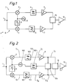
- an incoming radio signal on Node 1 is applied to two channels, an in-phase channel I, and a Quadrature-phase channel Q. Both channels are substantially identical and comprise a respective mixer 2, 3, channel filter 4, 5, and a limiting amplifiers 6, 7.
- a local oscillator 8 is applied directly to the inphase mixer 2 and via 90° phase shift circuit 9 to the Quadrature-Phase mixer 3.
- the limiting amplifiers 6, 7 remove the amplitude information from the signals and produce digital output signals containing only phase information.
- These signals are applied to a detector 10.
- the output of detector 10 is passed through limiting amplifier 11 to produce a detected base-band signal at its output 12. If necessary, amplifier 11 may incorporate a post-detection filter, not shown.
- Channel filters 4 and 5 serve to reject unwanted spurious signals from the output 5 of the mixers, and both I and Q channels are ideally identical so as to avoid any additional phase shift.
- the two signals applied to the inputs of detector 10 therefore always lead or lag each other by 90°.
- AFC Automatic Frequency Control
- a frequency detector comprises a first node arranged to receive a first signal which is a function of the input signal, a second node arranged to receive a second signal which is a function of the input signal, third and fourth nodes, phase shift means arranged to couple the first and second nodes to the third and fourth nodes respectively and to provide a first phase shift between the first and third nodes and a second phase shift between the second and fourth nodes, the phase shift means being such that the difference between the first and second phase shifts varies as a function of frequency, and phase detector means coupled to the third and fourth nodes and arranged to produce an output signal which is a function of the said difference, whereby said output signal is a function of the frequency of the input signal.
- a detector in accordance with the invention is used to provide a zero IF FSK radio receiver having automatic frequency control.
- the receiver has I and Q channels.
- the mixers 2, 3, limiting amplifiers 6, 7, and phase shift circuit 9, detector 10 and the amplifier 11 are substantially identical with correspondingly-numbered items in Figure 1.
- Detector 104 comprises an Exclusive-Or (EX-OR) gate.
- Filter 103 removes the AC component from the output on 104 and applies the DC component of the EX-OR output signal to VCO 102 which constitutes the local oscillator of the receiver.
- filters 100 and 101 of Figure 2 are not identical with each other but are specifically designed to have mutually different frequency-phase characteristics.
- the characteristics are such that, when oscillator 102 is at the correct frequency for receiving the incoming FSK signal at node 1, the signals at their respective outputs 110, 111 are exactly in quadrature. If the local oscillator frequency is too high, then 110 will differ from 111 by more than 90° for logic "1" and less than -90° for logic "0" and if too low, then 110 will differ from 111 by less than 90° for logic "1” and more than -90° for logic "0". This variation in phase difference with frequency is utilised to control the frequency of the local oscillator. The phase difference is detected by detector 104 whose mean DC output voltage varies as a function of the phase difference.
- the detector 104 is provided with a push-pull output stage which, in known manner, provides either pump-up or pump-down pulses which respectively incrementally tend to increase or decrease the DC voltage applied to a voltage-responsive element in VCO 102, the voltage being increased if the pump-up pulses predominate over the pump-down pulses, and decreased if the pump-down pulses predominate.
- the signals at output 110, 111 will, because of the effects of 100, 101, no longer be in quadrature but, as noted above, will deviate from quadrature by an amount which is a function of the discrepancy between the actual local oscillator frequency and its correct value. This deviation from quadrature will upset the balance between the pump-up and pump-down pulses, thereby causing a change in the DC output component of the EX-OR detector 104 in such a sense as to tend to return the output frequency of local oscillator 102 to its proper value.
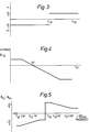
- a conventional Zero IF FSK receiver such as that illustrated in Figure 1, has the property that if the instantaneous frequency of the incoming RF signal, F sig , is greater than the LO frequency, F lo , then the I channel leads the Q channel by 90 degrees. If F sig is less than F lo then the I channel lags the Q channel by 90 degrees. This property is illustrated graphically in Figure 3. One way of demodulating the incoming signal is to determine which channel leads which by 90°.
- ⁇ F is the frequency for which the filters 100 and 101 produce the same phase shift.
- the exact respective characteristics of filters 100, 101 are not particularly important but for ease of explanation we shall assume a linear response as shown in the phase ⁇ ⁇ IQ versus frequency F IF plot of Figure 4.
- the outputs of the limiting amplifiers, signals I3 and Q3, provide the inputs to Exclusive-OR phase detector 104.
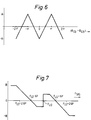
- the EX-OR's DC output voltage component versus phase difference ( ⁇ I3 - ⁇ Q3 ) is shown in Figure 6. Combining this with the phase difference ( ⁇ I3 - ⁇ Q3 ) versus frequency characteristic of Figure 5 gives the EX-OR phase detector's DC output voltage versus the instantaneous frequency of F sig , of the incoming FSK RF signal. This is shown in Figure 7.
- An incoming binary FSK signal jumps between one of two instantaneous frequencies depending on the data being transmitted: F c + ⁇ F corresponding to a logic "one” or F c - ⁇ F which corresponds to a logic "zero".
- F c is equal to F lo .
- F c F lo + F err
- F err offset frequency
- the invention has been described in terms of the instantaneous frequency, F sig , as being either at F c + ⁇ F (i.e. logic 1) or F c - ⁇ F (i.e. logic zero).
- the output of detector 104 in the transient case with an incoming signal being modulated by a random data stream can be approximated as a time-average of the detector's output for each of the instantaneous frequencies. This approximation is accurate for wideband FSK and still holds at low modulation indices.
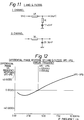
- Figure 11 shows an example of filter circuits suitable for inclusion in the I and Q channel filters 100, 101 to provide the required differential phase characteristics.
- the differential phase characteristics of the filters of Fig. 11 are shown in Fig. 12. It is to be noted that, while the filters of Fig. 11 per se are capable of providing satisfactory performance in respect of frequency control feedback, they may provide insufficient rejection for the data detector circuit 10. Accordingly the filters of Fig. 11 are preferably coupled in series with conventional matched filters, not shown separately, which are included in filters 100, 101 of Fig. 2.
- filters 4 and 5 are identical with the corresponding filters of Figure 1.
- the phase imbalance between the signals applied to the EX-OR detector 104 is provided by respective phase shift circuits 130, 131 coupled between the outputs of limiting amplifiers 6, 7 and the inputs of detector 104.
- This arrangement has the advantage that the outputs of signals 6 and 7 are maintained orthogonal at all times, ensuring that detector 10 is always provided with orthogonal signals. Operation is otherwise identical with Figure 2.
- one or the other of 130, 131 may be dispensed with, the necessary frequency-phase characteristic being provided by a single circuit 130, 131.
- further limiting amplifiers are disposed between filters 130, 131 and detector 104 to ensure that 104 is provided with logic signals of the correct levels.
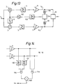
- Figure 14 shows a third embodiment which is a modification of Figure 13 and which can be used to overcome departures from true orthogonality in the local oscillator signals applied to mixers 2, 3. Only the relevant circuitry is shown, the rest of the circuit being as shown in Figure 13 or Figure 13 incorporating the unillustrated modifications referred to in the preceding paragraphs.
- This embodiment differs from Figure 13 in that it has a further EX-OR gate 144 and a subtracter 140 arranged to generate the difference between the outputs of 104 and 144.
- phase shift circuit 9 does not produce exactly 90° phase shift.
- the I and Q channels will not be exactly offset by 90°.
- the oscillator 102 happens to be operating at the correct frequency, the phase error induced by the phase shift error in 9 causes 104 to output a spurious error signal.
- Gate 144 generates a correction signal which is equal to the phase error signal component in the output of gate 104 produced by the phase shift circuit 9 per se.
- the correction signal is not responsive to the phase shifts produced by circuits 130, 131, and accordingly is unaffected by any error in the local oscillator frequency.
- the error produced by the phase shift circuit 9 is cancelled out and thus the signal applied to 103 represents only the error in frequency.
- Figure 15 is a modification of Figure 14.
- This embodiment of the invention differs from Figure 14 only in the provision of delay circuits 150, 151 which delay the signals applied to the inputs of 144.
- Delay circuits 150, 151 are matched, providing substantially identical delays. The delay is such that, in the absence of any error in phase shift circuit 9 or local oscillator frequency, the pulsating outputs of 104 and 144 are substantially exactly in-phase and cancel out. This can reduce the amount of filtering necessary in the AFC loop. Operation is otherwise identical with that of Figure 14.
- the embodiment of Figure 16 is a further modification of Figure 13.
- Adder 160 sums the I3 and Q3 signals and applies the result to filter 130.
- Subtracter 161 determines the difference between I3 and Q3 and applies the result to filter 131.
- filters 130 and 131 have different frequency-phase characteristics.
- the outputs of 130 and 131 are applied to EX-OR detector 104 via respective limiting amplifiers 164, 165.
- the output of detector 104 is applied to filter 103, not shown.
- the circuit is otherwise as shown in Figure 13.
- the Figure 16 embodiment has the property that the actual value of the phase shift produced by phase shift circuit 9, not shown, has no effect on the output of detector 104. Inspection of Fig.
- circuit elements in particular filters 100, 101, may be implemented digitally.
- filters 100, 101 may be implemented digitally.
- FIG 2 reference has been made to filters such as 101 and 102 having different phase characteristics, they could be replaced by substantially identical filters such as 4, 5 in series with all-pass circuits having mutually different phase characteristics. Similar comments apply to filters 130, 131 of Figures 14 to 16.
- any other suitable phase detector may be employed.
Landscapes
- Engineering & Computer Science (AREA)
- Physics & Mathematics (AREA)
- Spectroscopy & Molecular Physics (AREA)
- Computer Networks & Wireless Communication (AREA)
- Signal Processing (AREA)
- Power Engineering (AREA)
- Digital Transmission Methods That Use Modulated Carrier Waves (AREA)
- Circuits Of Receivers In General (AREA)
Applications Claiming Priority (2)
| Application Number | Priority Date | Filing Date | Title |
|---|---|---|---|
| GB9314841A GB2280324B (en) | 1993-07-16 | 1993-07-16 | Detectors |
| GB9314841 | 1993-07-16 |
Publications (2)
| Publication Number | Publication Date |
|---|---|
| EP0634855A1 true EP0634855A1 (fr) | 1995-01-18 |
| EP0634855B1 EP0634855B1 (fr) | 2002-05-08 |
Family
ID=10738997
Family Applications (1)
| Application Number | Title | Priority Date | Filing Date |
|---|---|---|---|
| EP94304624A Expired - Lifetime EP0634855B1 (fr) | 1993-07-16 | 1994-06-24 | Contrôle automatique de fréquence pour un récepteur de signaux modulés en sauts de fréquences, à conversion directe |
Country Status (6)
| Country | Link |
|---|---|
| US (1) | US5612976A (fr) |
| EP (1) | EP0634855B1 (fr) |
| JP (1) | JPH07154435A (fr) |
| CN (1) | CN1084995C (fr) |
| DE (1) | DE69430555T2 (fr) |
| GB (1) | GB2280324B (fr) |
Cited By (1)
| Publication number | Priority date | Publication date | Assignee | Title |
|---|---|---|---|---|
| US6973297B1 (en) | 1999-09-01 | 2005-12-06 | Sirific Wireless Corporation | Method and apparatus for down-conversion of radio frequency (RF) signals with reduced local oscillator leakage |
Families Citing this family (10)
| Publication number | Priority date | Publication date | Assignee | Title |
|---|---|---|---|---|
| JP3553286B2 (ja) * | 1995-09-21 | 2004-08-11 | セイコーインスツルメンツ株式会社 | Fsk復調回路 |
| JP2910695B2 (ja) * | 1996-08-30 | 1999-06-23 | 日本電気株式会社 | コスタスループ搬送波再生回路 |
| GB2330261B (en) * | 1997-10-09 | 2001-06-20 | Plessey Semiconductors Ltd | FSK Demodulator |
| US6304620B1 (en) * | 1998-03-20 | 2001-10-16 | Philips Electronics North America Corproation | Sign-cross product automatic frequency control loop |
| JP3568102B2 (ja) * | 1998-07-24 | 2004-09-22 | 松下電器産業株式会社 | 直接変換受信機 |
| US6738429B1 (en) | 1999-06-01 | 2004-05-18 | Harris Corporation | Decision-directed carrier frequency detector and method for QAM |
| US9297842B2 (en) | 2008-01-15 | 2016-03-29 | Nagasaki University, National University Corporation | Frequency detection device |
| CN102045284B (zh) * | 2010-01-21 | 2013-06-05 | 清华大学 | Fsk解调装置 |
| JP2011188428A (ja) * | 2010-03-11 | 2011-09-22 | Asahi Kasei Electronics Co Ltd | 送受信回路 |
| CN106656113A (zh) * | 2016-11-24 | 2017-05-10 | 北京无线电测量研究所 | 一种cmos差分调制脉冲检波电路及方法 |
Citations (2)
| Publication number | Priority date | Publication date | Assignee | Title |
|---|---|---|---|---|
| US4336616A (en) * | 1978-12-15 | 1982-06-22 | Nasa | Discriminator aided phase lock acquisition for suppressed carrier signals |
| EP0070695A2 (fr) * | 1981-07-16 | 1983-01-26 | International Standard Electric Corporation | Récepteur radio pour signaux à déplacement de fréquence |
Family Cites Families (5)
| Publication number | Priority date | Publication date | Assignee | Title |
|---|---|---|---|---|
| GB2180419A (en) * | 1985-09-16 | 1987-03-25 | Philips Electronic Associated | Direct conversion receiver |
| US5042052A (en) * | 1990-02-16 | 1991-08-20 | Harris Corporation | Carrier acquisition scheme for QAM and QPSK data |
| US5249204A (en) * | 1991-08-12 | 1993-09-28 | Motorola, Inc. | Circuit and method for phase error correction in a digital receiver |
| FR2680923B1 (fr) * | 1991-08-30 | 1996-11-22 | Patrick Vandamme | Dispositif de demodulation coherente a circuit numerique de recuperation d'onde porteuse. |
| FR2689712B1 (fr) * | 1992-04-03 | 1994-08-19 | Alcatel Telspace | Dispositif de démodulation de signaux numériques modulés selon une technique à constellations de modulation alternées. |
-
1993
- 1993-07-16 GB GB9314841A patent/GB2280324B/en not_active Expired - Fee Related
-
1994
- 1994-06-24 EP EP94304624A patent/EP0634855B1/fr not_active Expired - Lifetime
- 1994-06-24 DE DE69430555T patent/DE69430555T2/de not_active Expired - Fee Related
- 1994-07-11 US US08/272,839 patent/US5612976A/en not_active Expired - Lifetime
- 1994-07-14 JP JP6185365A patent/JPH07154435A/ja active Pending
- 1994-07-16 CN CN94108397A patent/CN1084995C/zh not_active Expired - Lifetime
Patent Citations (2)
| Publication number | Priority date | Publication date | Assignee | Title |
|---|---|---|---|---|
| US4336616A (en) * | 1978-12-15 | 1982-06-22 | Nasa | Discriminator aided phase lock acquisition for suppressed carrier signals |
| EP0070695A2 (fr) * | 1981-07-16 | 1983-01-26 | International Standard Electric Corporation | Récepteur radio pour signaux à déplacement de fréquence |
Non-Patent Citations (2)
| Title |
|---|
| CARSON L. M. ET AL.:: "Discriminator Aids Phase-Lock Acquisition", N.T.I.S. TECH NOTES, PART B, no. 11, November 1985 (1985-11-01), SPRINGFIELD, VA, US, pages 1290 * |
| HOLMES J. K.:: "Tracking-Loop Bias Due to Costas Loop Arm Filter Imbalance", IEEE TRANSACTIONS ON COMMUNICATIONS, vol. 30, no. 10, October 1982 (1982-10-01), NEW YORK, US, pages 2271 - 2273 * |
Cited By (3)
| Publication number | Priority date | Publication date | Assignee | Title |
|---|---|---|---|---|
| US6973297B1 (en) | 1999-09-01 | 2005-12-06 | Sirific Wireless Corporation | Method and apparatus for down-conversion of radio frequency (RF) signals with reduced local oscillator leakage |
| US7016662B1 (en) | 1999-09-01 | 2006-03-21 | Sirific Wireless Corporation | Method and apparatus for up-conversion of radio frequency (RF) signals |
| US7046980B1 (en) | 1999-09-01 | 2006-05-16 | Sirific Wireless Corporation | Method and apparatus for up-and down-conversion of radio frequency (RF) signals |
Also Published As
| Publication number | Publication date |
|---|---|
| GB2280324B (en) | 1998-07-22 |
| GB9314841D0 (en) | 1993-09-01 |
| GB2280324A (en) | 1995-01-25 |
| DE69430555D1 (de) | 2002-06-13 |
| CN1104820A (zh) | 1995-07-05 |
| DE69430555T2 (de) | 2002-08-29 |
| EP0634855B1 (fr) | 2002-05-08 |
| CN1084995C (zh) | 2002-05-15 |
| US5612976A (en) | 1997-03-18 |
| JPH07154435A (ja) | 1995-06-16 |
Similar Documents
| Publication | Publication Date | Title |
|---|---|---|
| US5584068A (en) | Direct conversion receiver | |
| CA2014916C (fr) | Recepteur a conversion directe avec variation de la frequence de l'oscillateur local dans la recherche de la frequence de porteuse | |
| US5809088A (en) | Digital carrier wave restoring device and method for use in a television signal receiver | |
| GB2040615A (en) | Receiver system | |
| US5612976A (en) | Detectors | |
| US4105975A (en) | Offset correction circuit for phase detectors | |
| JPS58500189A (ja) | 改良された位相同期を具えた位相同期ル−プ装置 | |
| US5659263A (en) | Circuit and method for correcting phase error in a multiplier circuit | |
| US4549142A (en) | Phase demodulator including variable phase shifter for controlling reference carrier | |
| US7227912B2 (en) | Receiver with mirror frequency suppression | |
| EP0638992B1 (fr) | Circuit démodulateur de fréquence | |
| US7079598B2 (en) | Complex phase-locked loop demodulator for low-IF and zero-IF radio receivers | |
| EP0217457B1 (fr) | Démodulateur d'oscillations modulées en angle | |
| US6525568B2 (en) | Circuit for the demodulation of the logic signal transmitted by analog channels | |
| EP0599414B1 (fr) | Récepteur à conversion directe | |
| FI97662B (fi) | Menetelmä kantoaallon palauttamiseksi | |
| GB2207582A (en) | Phase error correction and carrier recovery | |
| JP3254009B2 (ja) | 位相固定ループを含む回路 | |
| US6091789A (en) | Method and device for phase modulated signals | |
| JP2791402B2 (ja) | 周波数安定化回路 | |
| JPH0846433A (ja) | ビデオ信号復調回路 | |
| JP3462277B2 (ja) | 搬送波再生回路 | |
| GB2214742A (en) | Noise-controlled frequency-modulation signal detector | |
| HK1012803B (en) | A direct conversion receiver | |
| JPH0438041A (ja) | ロツク検出回路 |
Legal Events
| Date | Code | Title | Description |
|---|---|---|---|
| PUAI | Public reference made under article 153(3) epc to a published international application that has entered the european phase |
Free format text: ORIGINAL CODE: 0009012 |
|
| AK | Designated contracting states |
Kind code of ref document: A1 Designated state(s): DE FR |
|
| 17P | Request for examination filed |
Effective date: 19950707 |
|
| RAP1 | Party data changed (applicant data changed or rights of an application transferred) |
Owner name: MITEL SEMICONDUCTOR LIMITED |
|
| 17Q | First examination report despatched |
Effective date: 19981229 |
|
| GRAG | Despatch of communication of intention to grant |
Free format text: ORIGINAL CODE: EPIDOS AGRA |
|
| GRAG | Despatch of communication of intention to grant |
Free format text: ORIGINAL CODE: EPIDOS AGRA |
|
| GRAH | Despatch of communication of intention to grant a patent |
Free format text: ORIGINAL CODE: EPIDOS IGRA |
|
| GRAH | Despatch of communication of intention to grant a patent |
Free format text: ORIGINAL CODE: EPIDOS IGRA |
|
| GRAA | (expected) grant |
Free format text: ORIGINAL CODE: 0009210 |
|
| RAP1 | Party data changed (applicant data changed or rights of an application transferred) |
Owner name: ZARLINK SEMICONDUCTOR LIMITED |
|
| AK | Designated contracting states |
Kind code of ref document: B1 Designated state(s): DE FR |
|
| REF | Corresponds to: |
Ref document number: 69430555 Country of ref document: DE Date of ref document: 20020613 |
|
| ET | Fr: translation filed | ||
| PLBE | No opposition filed within time limit |
Free format text: ORIGINAL CODE: 0009261 |
|
| STAA | Information on the status of an ep patent application or granted ep patent |
Free format text: STATUS: NO OPPOSITION FILED WITHIN TIME LIMIT |
|
| 26N | No opposition filed |
Effective date: 20030211 |
|
| PGFP | Annual fee paid to national office [announced via postgrant information from national office to epo] |
Ref country code: FR Payment date: 20030610 Year of fee payment: 10 |
|
| PGFP | Annual fee paid to national office [announced via postgrant information from national office to epo] |
Ref country code: DE Payment date: 20030707 Year of fee payment: 10 |
|
| PG25 | Lapsed in a contracting state [announced via postgrant information from national office to epo] |
Ref country code: DE Free format text: LAPSE BECAUSE OF NON-PAYMENT OF DUE FEES Effective date: 20050101 |
|
| PG25 | Lapsed in a contracting state [announced via postgrant information from national office to epo] |
Ref country code: FR Free format text: LAPSE BECAUSE OF NON-PAYMENT OF DUE FEES Effective date: 20050228 |
|
| REG | Reference to a national code |
Ref country code: FR Ref legal event code: ST |