EP0627770B1 - Spannungsgesteuerter Photodetektor - Google Patents
Spannungsgesteuerter Photodetektor Download PDFInfo
- Publication number
- EP0627770B1 EP0627770B1 EP94302584A EP94302584A EP0627770B1 EP 0627770 B1 EP0627770 B1 EP 0627770B1 EP 94302584 A EP94302584 A EP 94302584A EP 94302584 A EP94302584 A EP 94302584A EP 0627770 B1 EP0627770 B1 EP 0627770B1
- Authority
- EP
- European Patent Office
- Prior art keywords
- quantum well
- multiple quantum
- well layer
- layer
- photodetector
- Prior art date
- Legal status (The legal status is an assumption and is not a legal conclusion. Google has not performed a legal analysis and makes no representation as to the accuracy of the status listed.)
- Expired - Lifetime
Links
Images
Classifications
-
- B—PERFORMING OPERATIONS; TRANSPORTING
- B82—NANOTECHNOLOGY
- B82Y—SPECIFIC USES OR APPLICATIONS OF NANOSTRUCTURES; MEASUREMENT OR ANALYSIS OF NANOSTRUCTURES; MANUFACTURE OR TREATMENT OF NANOSTRUCTURES
- B82Y20/00—Nanooptics, e.g. quantum optics or photonic crystals
-
- H—ELECTRICITY
- H10—SEMICONDUCTOR DEVICES; ELECTRIC SOLID-STATE DEVICES NOT OTHERWISE PROVIDED FOR
- H10F—INORGANIC SEMICONDUCTOR DEVICES SENSITIVE TO INFRARED RADIATION, LIGHT, ELECTROMAGNETIC RADIATION OF SHORTER WAVELENGTH OR CORPUSCULAR RADIATION
- H10F30/00—Individual radiation-sensitive semiconductor devices in which radiation controls the flow of current through the devices, e.g. photodetectors
- H10F30/20—Individual radiation-sensitive semiconductor devices in which radiation controls the flow of current through the devices, e.g. photodetectors the devices having potential barriers, e.g. phototransistors
- H10F30/21—Individual radiation-sensitive semiconductor devices in which radiation controls the flow of current through the devices, e.g. photodetectors the devices having potential barriers, e.g. phototransistors the devices being sensitive to infrared, visible or ultraviolet radiation
- H10F30/22—Individual radiation-sensitive semiconductor devices in which radiation controls the flow of current through the devices, e.g. photodetectors the devices having potential barriers, e.g. phototransistors the devices being sensitive to infrared, visible or ultraviolet radiation the devices having only one potential barrier, e.g. photodiodes
- H10F30/223—Individual radiation-sensitive semiconductor devices in which radiation controls the flow of current through the devices, e.g. photodetectors the devices having potential barriers, e.g. phototransistors the devices being sensitive to infrared, visible or ultraviolet radiation the devices having only one potential barrier, e.g. photodiodes the potential barrier being a PIN barrier
-
- H—ELECTRICITY
- H10—SEMICONDUCTOR DEVICES; ELECTRIC SOLID-STATE DEVICES NOT OTHERWISE PROVIDED FOR
- H10F—INORGANIC SEMICONDUCTOR DEVICES SENSITIVE TO INFRARED RADIATION, LIGHT, ELECTROMAGNETIC RADIATION OF SHORTER WAVELENGTH OR CORPUSCULAR RADIATION
- H10F77/00—Constructional details of devices covered by this subclass
- H10F77/10—Semiconductor bodies
- H10F77/14—Shape of semiconductor bodies; Shapes, relative sizes or dispositions of semiconductor regions within semiconductor bodies
- H10F77/146—Superlattices; Multiple quantum well structures
-
- H—ELECTRICITY
- H10—SEMICONDUCTOR DEVICES; ELECTRIC SOLID-STATE DEVICES NOT OTHERWISE PROVIDED FOR
- H10F—INORGANIC SEMICONDUCTOR DEVICES SENSITIVE TO INFRARED RADIATION, LIGHT, ELECTROMAGNETIC RADIATION OF SHORTER WAVELENGTH OR CORPUSCULAR RADIATION
- H10F77/00—Constructional details of devices covered by this subclass
- H10F77/30—Coatings
- H10F77/306—Coatings for devices having potential barriers
Definitions
- the present invention generally relates to monolithic integrated circuit technology and electromagnetic communication technology and, more particularly, to a tunable monolithic integrated photodetector for detecting light at a selected wavelength within a wavelength range.
- Photocurrent refers to the flow of electrons or holes within the material.
- a peak in the photocurrent spectrum of the material which results from the absorption of photons is oftentimes referred to as an exciton.
- a multiple quantum well (MQW) diode can be used as a photodetector whose voltage of maximum photocurrent, i.e ., a large exciton, is dependent upon the wavelength of incident light.
- MQW multiple quantum well
- An MQW material is essentially a narrow bandgap material which has a thickness substantially less than the diameter of an exciton and which is sandwiched between wider bandgap materials so as to enhance the exciton via confinement of the energy potential well.
- the voltage of maximum photocurrent within the MQW diode can be located and related to the wavelength of the incident light, thereby allowing for measurements of the wavelength. Identifying the wavelength of incident light is beneficial in imaging and spectroscopy applications.
- the light incident on a photosensitive material can create multiple peaks in the photocurrent spectrum, that is, more than one exciton.
- the photocurrent exhibits a relatively large exciton, called a heavy hole (hh) exciton, at the particular wavelength of incident light, as well as any number of smaller excitons, called light hole (lh) excitons, at other wavelengths of the photocurrent spectrum.
- hh heavy hole
- lh light hole
- the selectivity of an MQW diode is step-like, producing photocurrent at all photon wavelengths at and above the exciton wavelength. If no electrical bias is applied to the MQW diode, the peak-to-valley ratio of the hh exciton to the lh exciton is typically about 1.3 to 1 and reduces considerably with applied bias. See A.M. Fox et al ., “Quantum Well Carrier Sweep Out; Relation to Electroabsorption and Exciton Saturation,” IEEE Journal of Quantum Electronics , vol. 27, p. 2281 (1991).
- the lh excitons become indistinguishable from the hh excitons.
- the photocurrent peak at the lh exciton is actually larger than the peak at the hh exciton and occurs at the same wavelength as the hh exciton at 0 V/ ⁇ m bias.
- EP-A-0385 803 discloses a monolithic integrated semiconductor optical element having a n-i-p-i-n structure comprising two stacked quantum well structures as optical absorption layers to detect a plurality of monochromatic signals.
- the first MQW element is biased to detect and absorb the signal having the longest wavelength and passes the remaining signals to the next MQW element. It is suggested that the bias voltages applied to the elements might be controlled to adjust the characteristics of the elements.
- the present invention is a tunable monolithic integrated photodetector for detecting light at a selected wavelength within a wavelength range.
- the photodetector comprises a filter means, a detector means, and a bias means. Both the filter means and the detector means are formed from multiple quantum well (MQW) materials which are monolithically integrated atop a substrate.
- the filter means (first MQW layer) receives and filters incident light, and the detector means (second MQW layer) receives light from the filter means and detects the selected wavelength.
- the bias means applies a fixed bias and a variable bias.
- the fixed bias is applied between the filter means and the detector means for the purpose of causing the filter means to absorb light wavelengths surrounding the selected wavelength, thereby enhancing the detectability of the selected wavelength by the detector means.
- the variable bias is applied proportionally to both the filter means and the detector means for specifying, in effect, the selected wavelength within the tunable range.
- a fixed filter may also be implemented for filtering out wavelengths of incident light beyond the tunable range of the photodetector. Optimal selectivity is achieved utilizing the fixed filter in combination with the photodetector.
- a plurality of photodetectors formed in accordance with the present invention may be situated in a plane to form a two-dimensional array.
- the array of photodetectors may be used for many purposes, including imaging applications.
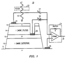
- a monolithic integrated photodetector 10 residing on a substrate 11 can determine the wavelength of incident light 12.
- the monolithic integrated photodetector 10 is preferably a n-i(MQW)-p-i(MQW)-n device with independent contacts to each of the p and n doped layers.
- the photodetector 10 comprises the following successive layers: an n-doped layer 13, an intrinsic MQW layer 14 serving as a filter means, a p-doped layer 15, an intrinsic second MQW layer 16 serving as a detector means for detecting the wavelength of the incident light 12, and the n-doped substrate 11.
- a fixed voltage bias V ⁇ is applied between the MQW filter means 14 and the MQW detector means 16 via a fixed voltage source 17 of Fig. 1.
- the voltage source 17 is connected between a contact 21 on the top surface of the n-doped layer 13 and a buffer 24, which will be described in further detail hereinafter.
- the fixed voltage bias V ⁇ causes the MQW filter means 14 to absorb light wavelengths substantially surrounding the selected wavelength to thereby enhance the detectability of the selected wavelength.
- the photocurrent spectrum of the MQW detector means 16 is slightly shifted compared to that of the MQW filter means 14. This predicament creates a narrow wavelength region where detectability is maximized, thus closely approximating a single wavelength, voltage tunable photodetector.
- a variable voltage bias V p is proportionally applied by a variable voltage source 18 across both the MQW filter means 14 and MQW detector means 16.
- the voltage source 18 is connected between a contact 22 and the buffer 24.
- the contact 22 is situated in a well through the n-doped layer 13 and MQW filter means 14 to the p-doped layer 15.
- the photodetector 10 is tuned. In other words, as the voltage bias V p is varied, the wavelength at which the MQW detector means 16 will exhibit a heavy hole exciton from the incident light 12 is varied.
- the buffer 24 preferably a current preamplifier having resistor R and operational amplifier OPAMP, is connected to the positive terminals of the voltage sources 17, 18 and to the substrate 11 via contact 25 in order to provide a photodetector output 26. Photocurrent generated in the MQW filter means 14 does not flow through the buffer 24, but rather is shunted through the voltage sources 17, 18.
- the photodetector 10 is formed on an n-doped GaAs substrate 11 using GaAs-source molecular beam epitaxy.
- 0.5 ⁇ m of n-doped Al 0.3 Ga 0.7 As is formed on the GaAs substrate 11.
- the MQW detector means 16 is formed on the foregoing layer.
- the MQW detector 16 preferably comprises 75 undoped periods of 95 ⁇ GaAs wells and 45 ⁇ Al 0.3 Ga 0.7 As barriers.
- the MQW detector means 16 is then clad with 200 ⁇ Al 0.3 Ga 0.7 As spacers on both sides.
- a 0.8 ⁇ m p-doped Al 0.3 Ga 0.7 As layer 15 is formed on the MQW detector means 16.
- the MQW filter means 14 is formed on the doped layer 15.
- the MQW filter means 14 preferably comprises 71 undoped periods of 95 ⁇ GaAs wells and 45 ⁇ Al 0.3 Ga 0.7 As barriers.
- the MQW filter means 14 is clad with 200 ⁇ Al 0.3 Ga 0.7 As undoped spacers.
- a 0.6 ⁇ m Al 0.3 Ga 0.7 As n-doped layer 13 is formed on the MQW filter means 14, followed by a 50 ⁇ n+doped GaAs cap layer.
- the MQW filter means 14 has fewer periods than the MQW detector means 16 so that the MQW filter means 14 red shifts faster with voltage and thus tends to maintain the difference of the red shifts of the filter means 14 and the detector means 16 constant if the fixed voltage bias V ⁇ is kept fixed. Otherwise, the difference would not increase proportionally because the red shift is quadratic with respect to field strength.
- a "red shift" in the context of this document means a shift in the photocurrent spectrum of a material, and thus, a change in the photon energy for generating excitons. With the preceding configuration, tunability is achieved by varying only the bias V p supplied by voltage source 18.
- the fixed voltage source 17 for supplying the fixed voltage bias V ⁇ could be replaced by a variable voltage source.
- the MQW filter means 14 would not need to have fewer periods than the MQW detector means 16.
- more than one voltage source would need to be adjusted in order to tune the photodetector 10, thus making this circuit configuration undesirable.
- a AuGe layer is placed photolithographically on the n-doped layer 13 to form the contact 21.
- a self-aligned technique is used to place the contact 22 within the well 23 on the p-doped layer 15.
- the reason for using a self-aligned technique is that care must be taken to avoid exposing regions of the MQW detector means 16 to light which is unfiltered by the MQW filter means 14.
- openings are defined in a layer of photoresist, and the sample is etched through the photoresist layer to the p-doped layer 15.
- An AuZn layer is then deposited onto the p-doped layer 15 using the same photoresist mask for the lift-off in order to form the contact 22.
- the entire etched region is coated with metal, as illustrated in Fig. 1. Because the contact 22 is deposited using the foregoing procedure, the photodetector 10 functions without having to focus the incident light 12 on any particular area of the n-doped layer 13. Finally, a mesa configuration for the photodetector 10 is formed by etching the structure down to the bottom n-doped substrate 11.
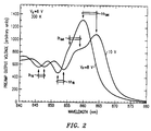
- Fig. 2 is a graph showing the photodetector output 26, i.e ., preamp output voltage, versus wavelength of incident light 12 with the fixed voltage bias V ⁇ set at about 6 volts and the variable voltage bias V p set at about 8 volts and at about 10 volts during separate trials.
- the spectrum of Fig. 2 was generated by applying an unfocused light source over the mesa configuration.
- the heavy hole (hh) and light hole (lh) excitons of the MQW detector means 16 show up as peaks in the spectrum, while the heavy hole and light hole excitons of the MQW filter means 14 show up as dips.
- the peak-to-valley ratio of the detector peaks compared to the remainder of the spectrum is enhanced dramatically.
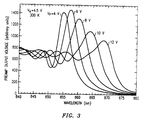
- Fig. 3 is a graph of the photodetector output 26 versus wavelength of incident light 12 with the fixed voltage bias V ⁇ set at about 4.5 volts and the variable voltage bias V p set at about 4, 6, 8, 10 and 12 volts on separate trials.
- the difference between the red shifts of the detector means 16 and the filter means 14 are smaller than in Fig. 2, giving a more distinguished single peak for wavelength.
- the heavy hole exciton of the MQW filter means 14 lies approximately on the light hole exciton of the MQW detector means 16, thus having maximum effect at removing signals at wavelengths other than at the wavelength of the heavy hole exciton of the MQW detector means 16. With these settings, a tuning range of at least approximately 14 nm is achieved.
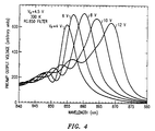
- a fixed filter 27 may be employed to filter the incident light 12.
- the fixed filter 27 eliminates all wavelengths of light outside of the tunable range of the photodetector 10.
- a suitable fixed filter 27 is a model RG.850 filter manufactured by and commercially available from Newport, Inc., California, U.S.A.
- the RG.850 filter exhibits greater than 95% transmission for light with wavelengths longer than 900 nm, and decreases to less than about 0.1% transmission for light with wavelengths less than 800 nm with a smooth transition thereinbetween.
- Fig. 4 shows the photodetector output 26 versus wavelength of incident light 12 with the fixed voltage bias V ⁇ set at about 4.5 volts, the variable voltage bias V p set at about 4, 6, 8, 10, and 12 volts during separate trials, and the fixed filter 27.
- the fixed filter 27 achieves very good selectivity, and the maximum voltage response is fairly constant as a function of the variable voltage bias V p .
- the ratio of the maximum response for V p at 869 nm in Fig. 4 to the response in the spurious peak for the photodetector output 26 at 857 nm is about 1.9 to 1. Because this spurious peak is about the maximum response position of the V p equal 4 volt curve, this ratio is a good measure of the wavelength selectivity of the photodetector 10.
- a plurality of the photodetectors 10 of Fig. 1 may be situated in a two dimensional array for spectroscopy and imaging applications. In this application, each of the photodetectors 10 would detect a particular element of an image exposed to the array.
Landscapes
- Chemical & Material Sciences (AREA)
- Engineering & Computer Science (AREA)
- Nanotechnology (AREA)
- Physics & Mathematics (AREA)
- Life Sciences & Earth Sciences (AREA)
- Biophysics (AREA)
- Optics & Photonics (AREA)
- Crystallography & Structural Chemistry (AREA)
- Light Receiving Elements (AREA)
Claims (9)
- Abstimmbarer monolithischer integrierter Fotodetektor mit einer grundlegenden n-i-p-i-n-Schichtstruktur, der folgendes umfaßt:eine erste Mehrfach-Quantentopf-Schicht (14) (14) mit einem ersten Fotostromspektrum zum Empfangen und Filtern von auftreffendem Licht, wobei die Mehrfach-Quantentopf-Schicht (14) eine erste Fläche (13) zum Empfangen des auftreffenden Lichts und eine zweite Fläche aufweist;eine zweite Mehrfach-Quantentopf-Schicht (16) mit einem zweiten Fotostromspektrum zum Empfangen und Erfassen von auftreffendem Licht, das von der ersten Mehrfach-Quantentopf-Schicht durchgelassen wurde, wobei die zweite Mehrfach-Quantentopf-Schicht (16) eine erste Fläche aufweist;Elektrodenmittel (21, 22, 25), die jeweils mit der ersten und zweiten Mehrfach-Quantentopf-Schicht verbunden sind, und Mittel (17) zum Anlegen einer festen Vorspannung an die erste Mehrfach-Quantentopf-Schicht mit Hilfe einer an der ersten Fläche (13) der ersten Mehrfach-Quantentopf-Schicht (14) angebrachten ersten Elektrode (21);
dadurch gekennzeichnet, daßein veränderbares Vorspannungsmittel (18) mit einer zweiten Elektrode (22) verbunden ist, die mit der Grenzfläche (15) der zweiten Fläche der ersten Mehrfach-Quantentopf-Schicht und der ersten Fläche der zweiten Mehrfach-Quantentopf-Schicht verbunden ist, um eine Vorspannung sowohl an die erste als auch die zweite Mehrfach-Quantentopf-Schicht anzulegen, wobei das veränderbare Vorspannungsmittel seriell entgegengesetzt zu dem festen Vorspannungsmittel angeschlossen ist;
wobei die erste Mehrfach-Quantentopf-Schicht (14) weniger Perioden umfaßt als die zweite Mehrfach-Quantentopf-Schicht (16); unddas feste Vorspannungsmittel angeordnet ist, um eine derartige Vorspannung anzulegen, daß das Fotostromspektrum der zweiten Mehrfach-Quantentopf-Schicht (16) relativ zu dem Fotostromspektrum der ersten Mehrfach-Quantentopf-Schicht (14) verschoben wird, wodurch die erste Mehrfach-Quantentopf-Schicht Licht-Loch-Exzitonen in dem der zweiten Mehrfach-Quantentopf-Schicht entsprechenden Fotostromspektrum auf ein Mimimum reduziert. - Fotodetektor nach Anspruch 1, bei dem die erste Mehrfach-Quantentopf-Schicht der zweiten Mehrfach-Quantentopf-Schicht überlagert ist, die einem Substrat (11) überlagert ist.
- Fotodetektor nach Anspruch 1, weiterhin mit einem festen Filter (27) zum Eliminieren von Wellenlängen des auftreffenden Lichts, die außerhalb des Bereichs des Fotodetektors liegen.
- Mehrere Fotodetektoren, die gemäß dem Fotodetektor von Anspruch 1 ausgebildet sind, wobei die mehreren Fotodetektoren in einem Array angeordnet sind.
- Fotodetektor nach Anspruch 2, weiterhin mit einer ersten dotierten Schicht (15) zwischen der ersten und zweiten Mehrfach-Quantentopf-Schicht, einer zweiten dotierten Schicht (13) auf der ersten Mehrfach-Quantentopf-Schicht zum Empfangen des auftreffenden Lichts und einer dritten dotierten Schicht zwischen der zweiten Mehrfach-Quantentopf-Schicht und dem Substrat.
- Fotodetektor nach Anspruch 5, weiterhin mit einem offenen Topf durch die zweite dotierte Schicht (13) und die erste Mehrfach-Quantentopf-Schicht (14) zu der ersten dotierten Schicht (15) und wobei der Topf einen elektrischen Kontakt (22) zum Anlegen einer Vorspannung an die erste dotierte Schicht umfaßt.
- Fotodetektor nach Anspruch 5, wobei die erste dotierte Schicht ein p-dotiertes Material und die zweite und dritte dotierte Schicht jeweils n-dotiertes Material umfassen.
- Verfahren zum Verwenden eines Fotodetektors nach Anspruch 1 zum Erfassen von Licht mit einer gewählten Wellenlänge innerhalb eines Wellenlängenbereichs,
gekennzeichnet durchproportionales Verändern der veränderbaren Vorspannung, um die gewählte Wellenlänge zu wählen und die gewählte Wellenlänge durch den Bereich zu bewegen; undBereitstellen der festen Vorspannung, um die an die erste Mehrfach-Quantentopf-Schicht angelegte Vorspannung relativ zu der an die zweite Mehrfach-Quantentopf-Schicht angelegten zu versetzen, um das Absorptionsspektrum der ersten Mehrfach-Quantentopf-Schicht in Richtung von kürzeren Wellenlängen relativ zu dem der zweiten Mehrfach-Quantentopf-Schicht zu verschieben und auf diese Weise die Erfaßbarkeit der gewählten Wellenlänge innerhalb des Bereichs durch die zweite Mehrfach-Quantentopf-Schicht zu verbessern. - Verfahren nach Anspruch 8, weiterhin mit dem Schritt des Filterns des auftreffenden Lichts durch Eliminieren von Wellenlängen des auftreffenden Lichts, die außerhalb des Bereichs des Fotodetektors liegen, um auf diese Weise die Erfaßbarkeit der gewählten Wellenlänge zu verbessern.
Applications Claiming Priority (2)
| Application Number | Priority Date | Filing Date | Title |
|---|---|---|---|
| US56374 | 1993-04-30 | ||
| US08/056,374 US5329136A (en) | 1993-04-30 | 1993-04-30 | Voltage-tunable photodetector |
Publications (2)
| Publication Number | Publication Date |
|---|---|
| EP0627770A1 EP0627770A1 (de) | 1994-12-07 |
| EP0627770B1 true EP0627770B1 (de) | 2000-07-12 |
Family
ID=22003967
Family Applications (1)
| Application Number | Title | Priority Date | Filing Date |
|---|---|---|---|
| EP94302584A Expired - Lifetime EP0627770B1 (de) | 1993-04-30 | 1994-04-13 | Spannungsgesteuerter Photodetektor |
Country Status (5)
| Country | Link |
|---|---|
| US (1) | US5329136A (de) |
| EP (1) | EP0627770B1 (de) |
| JP (1) | JP2716364B2 (de) |
| CA (1) | CA2108096C (de) |
| DE (1) | DE69425192T2 (de) |
Families Citing this family (30)
| Publication number | Priority date | Publication date | Assignee | Title |
|---|---|---|---|---|
| KR0125014B1 (ko) * | 1993-07-15 | 1997-12-01 | 양승택 | 초고속 광스위칭 소자 |
| US5459332A (en) * | 1994-03-31 | 1995-10-17 | The United States Of America As Represented By The Secretary Of The Navy | Semiconductor photodetector device |
| CA2156333C (en) * | 1994-09-28 | 1999-03-23 | John Edward Cunningham | Optoelectronic devices utilizing multiple quantum well pin structures and a process for fabricating the same |
| FR2738097B1 (fr) * | 1995-08-22 | 1997-09-26 | Thomson Csf | Dispositif optronique d'aide au pilotage de nuit pour aeronefs |
| US6130466A (en) * | 1995-10-17 | 2000-10-10 | Fraunhofer Gesellschaft Zur Foerderung Der Angewandten Forschung E.V. | Semiconductor heterostructure radiation detector having two spectral sensitivity ranges |
| US5872016A (en) * | 1996-06-18 | 1999-02-16 | Lucent Technologies Inc. | Process of making an optoelectronic devices utilizing multiple quantum well pin structures |
| KR19980050460A (ko) * | 1996-12-20 | 1998-09-15 | 양승택 | 다중 파장 동시 인식을 위한 광검출기 구조 및 그를 이용한 광검출방법 |
| US5747861A (en) * | 1997-01-03 | 1998-05-05 | Lucent Technologies Inc. | Wavelength discriminating photodiode for 1.3/1.55 μm lightwave systems |
| DE19723177A1 (de) * | 1997-06-03 | 1998-12-10 | Daimler Benz Ag | Spannungsgesteuerter wellenlängenselektiver Photodetektor |
| JP3542965B2 (ja) * | 1997-10-16 | 2004-07-14 | カリフォルニア インスティチュート オブ テクノロジー | デュアルバンド量子井戸赤外線センシングアレイ |
| US6043549A (en) * | 1998-03-20 | 2000-03-28 | Trw Inc. | Responsivity photodetector |
| US6054718A (en) * | 1998-03-31 | 2000-04-25 | Lockheed Martin Corporation | Quantum well infrared photocathode having negative electron affinity surface |
| US6355939B1 (en) | 1998-11-03 | 2002-03-12 | Lockheed Martin Corporation | Multi-band infrared photodetector |
| US6180990B1 (en) | 1999-03-26 | 2001-01-30 | Lockheed Martin Corporation | Hyperspectral radiation detector |
| FR2832512B1 (fr) * | 2001-11-16 | 2004-01-02 | Atmel Grenoble Sa | Composant de filtrage optique accordable |
| US6646318B1 (en) * | 2002-08-15 | 2003-11-11 | National Semiconductor Corporation | Bandgap tuned vertical color imager cell |
| US7135698B2 (en) * | 2002-12-05 | 2006-11-14 | Lockheed Martin Corporation | Multi-spectral infrared super-pixel photodetector and imager |
| US6897447B2 (en) * | 2002-12-05 | 2005-05-24 | Lockheed Martin Corporation | Bias controlled multi-spectral infrared photodetector and imager |
| IL155536A0 (en) * | 2003-04-21 | 2003-11-23 | Yissum Res Dev Co | Voltage tunable integrated infrared imager |
| TWI250659B (en) | 2003-07-31 | 2006-03-01 | Osram Opto Semiconductors Gmbh | Radiation-receiving semiconductor-body with an integrated filter-layer |
| DE10341086B4 (de) * | 2003-07-31 | 2007-06-06 | Osram Opto Semiconductors Gmbh | Strahlungsempfangender Halbleiterkörper mit einer Filterschicht |
| DE10345555A1 (de) | 2003-09-30 | 2005-05-04 | Osram Opto Semiconductors Gmbh | Strahlungsemittierendes und -empfangendes Halbleiterbauelement und Verfahren zu dessen Herstellung |
| TWI244768B (en) * | 2005-04-08 | 2005-12-01 | South Epitaxy Corp | Photodetector |
| WO2007126418A2 (en) * | 2006-03-27 | 2007-11-08 | The Regents Of The University Of California | Optically interface electrically controlled devices |
| IT1393542B1 (it) * | 2009-03-30 | 2012-04-27 | Milano Politecnico | Foto-rivelatore e metodo per rivelare una radiazione ottica |
| JP5628120B2 (ja) * | 2011-09-15 | 2014-11-19 | ローム株式会社 | 発光素子モジュール |
| JP6428091B2 (ja) * | 2014-09-24 | 2018-11-28 | 住友電気工業株式会社 | 赤外線イメージセンサ |
| US10381502B2 (en) * | 2015-09-09 | 2019-08-13 | Teledyne Scientific & Imaging, Llc | Multicolor imaging device using avalanche photodiode |
| TWI905261B (zh) * | 2021-09-09 | 2025-11-21 | 晶元光電股份有限公司 | 光電元件 |
| DE102021127038A1 (de) | 2021-10-19 | 2023-04-20 | OSRAM Opto Semiconductors Gesellschaft mit beschränkter Haftung | Detektorelement, lidar modul und verfahren zum betrieb eines lidar moduls |
Family Cites Families (8)
| Publication number | Priority date | Publication date | Assignee | Title |
|---|---|---|---|---|
| US4205331A (en) * | 1978-06-09 | 1980-05-27 | The United States Of America As Represented By The Secretary Of The Army | Infrared optical devices of layered structure |
| US4711857A (en) * | 1986-08-28 | 1987-12-08 | The United States Of America As Represented By The Administrator Of The National Aeronautics And Space Administration | Tailorable infrared sensing device with strain layer superlattice structure |
| US5023685A (en) * | 1988-06-06 | 1991-06-11 | Bethea Clyde G | Quantum-well radiation-interactive device, and methods of radiation detection and modulation |
| JPH02170581A (ja) * | 1988-12-23 | 1990-07-02 | Fujitsu Ltd | 半導体受光装置 |
| GB2228824A (en) * | 1989-03-01 | 1990-09-05 | Gen Electric Co Plc | Radiation detectors |
| US5144397A (en) * | 1989-03-03 | 1992-09-01 | Mitsubishi Denki Kabushiki Kaisha | Light responsive semiconductor device |
| US5229878A (en) * | 1990-07-02 | 1993-07-20 | Canon Kabushiki Kaisha | Method and apparatus for modulating light using semiconductor element having quantum well structure |
| JP2906713B2 (ja) * | 1991-03-29 | 1999-06-21 | 三菱電機株式会社 | 光素子の多重安定性取得方法 |
-
1993
- 1993-04-30 US US08/056,374 patent/US5329136A/en not_active Expired - Lifetime
- 1993-10-08 CA CA002108096A patent/CA2108096C/en not_active Expired - Fee Related
-
1994
- 1994-04-13 DE DE69425192T patent/DE69425192T2/de not_active Expired - Fee Related
- 1994-04-13 EP EP94302584A patent/EP0627770B1/de not_active Expired - Lifetime
- 1994-04-13 JP JP6097864A patent/JP2716364B2/ja not_active Expired - Fee Related
Also Published As
| Publication number | Publication date |
|---|---|
| CA2108096A1 (en) | 1994-10-31 |
| US5329136A (en) | 1994-07-12 |
| JPH06326345A (ja) | 1994-11-25 |
| DE69425192D1 (de) | 2000-08-17 |
| EP0627770A1 (de) | 1994-12-07 |
| JP2716364B2 (ja) | 1998-02-18 |
| CA2108096C (en) | 1997-09-30 |
| DE69425192T2 (de) | 2001-03-22 |
Similar Documents
| Publication | Publication Date | Title |
|---|---|---|
| EP0627770B1 (de) | Spannungsgesteuerter Photodetektor | |
| US4903101A (en) | Tunable quantum well infrared detector | |
| CA2038844C (en) | Multicolor infrared photodetector | |
| EP1040522B1 (de) | Zweiband infrarot quantentopf-detektoranordnung | |
| KR100359188B1 (ko) | 혼성의비대칭페브리페롯양자웰광변조기 | |
| KR100396628B1 (ko) | 광변환장치및방법과이미지변환기 | |
| US5646421A (en) | Multicolor voltage tunable quantum well intersubband infrared photodetector | |
| US5144397A (en) | Light responsive semiconductor device | |
| US6349156B1 (en) | Semiconductor etalon device, optical control system and method | |
| US6380604B1 (en) | Quantum semiconductor device having quantum dots and optical detectors using the same | |
| US6576490B2 (en) | Method for micro-fabricating a pixelless infrared imaging device | |
| US8111440B2 (en) | Structure and method for modulating light | |
| JP2007303927A (ja) | 光検出器 | |
| US5677544A (en) | Quantum well detector and process for the manufacture thereof | |
| US5926585A (en) | Waveguide type light receiving element | |
| Miller | Modeling and performance of wafer-fused resonant-cavity enhanced photodetectors | |
| US5637883A (en) | Optically addressed spatial light modulator using an intrinsic semiconductor active material and high resistivity cladding layers | |
| JP2000188407A (ja) | 赤外線検知素子 | |
| JP2000183319A (ja) | 量子井戸型光センサ | |
| US6693311B2 (en) | Wavelength selective detector | |
| Goossen et al. | Voltage‐tunable multiple quantum well photodetector vertically integrated with voltage‐tunable multiple quantum well filter | |
| JP4331428B2 (ja) | サブバンド間遷移量子井戸型光検知装置 | |
| JPH06204549A (ja) | 導波路型受光素子並びにその製造方法及びその駆動方法 | |
| JPH10144950A (ja) | 半導体受光デバイス | |
| JPH1065200A (ja) | 赤外受光素子 |
Legal Events
| Date | Code | Title | Description |
|---|---|---|---|
| PUAI | Public reference made under article 153(3) epc to a published international application that has entered the european phase |
Free format text: ORIGINAL CODE: 0009012 |
|
| AK | Designated contracting states |
Kind code of ref document: A1 Designated state(s): DE FR GB NL |
|
| 17P | Request for examination filed |
Effective date: 19950524 |
|
| 17Q | First examination report despatched |
Effective date: 19960227 |
|
| GRAG | Despatch of communication of intention to grant |
Free format text: ORIGINAL CODE: EPIDOS AGRA |
|
| GRAG | Despatch of communication of intention to grant |
Free format text: ORIGINAL CODE: EPIDOS AGRA |
|
| GRAG | Despatch of communication of intention to grant |
Free format text: ORIGINAL CODE: EPIDOS AGRA |
|
| GRAH | Despatch of communication of intention to grant a patent |
Free format text: ORIGINAL CODE: EPIDOS IGRA |
|
| GRAH | Despatch of communication of intention to grant a patent |
Free format text: ORIGINAL CODE: EPIDOS IGRA |
|
| GRAA | (expected) grant |
Free format text: ORIGINAL CODE: 0009210 |
|
| AK | Designated contracting states |
Kind code of ref document: B1 Designated state(s): DE FR GB NL |
|
| REF | Corresponds to: |
Ref document number: 69425192 Country of ref document: DE Date of ref document: 20000817 |
|
| ET | Fr: translation filed | ||
| PGFP | Annual fee paid to national office [announced via postgrant information from national office to epo] |
Ref country code: FR Payment date: 20010322 Year of fee payment: 8 |
|
| PGFP | Annual fee paid to national office [announced via postgrant information from national office to epo] |
Ref country code: GB Payment date: 20010326 Year of fee payment: 8 |
|
| PGFP | Annual fee paid to national office [announced via postgrant information from national office to epo] |
Ref country code: NL Payment date: 20010327 Year of fee payment: 8 |
|
| PLBE | No opposition filed within time limit |
Free format text: ORIGINAL CODE: 0009261 |
|
| STAA | Information on the status of an ep patent application or granted ep patent |
Free format text: STATUS: NO OPPOSITION FILED WITHIN TIME LIMIT |
|
| 26N | No opposition filed | ||
| PGFP | Annual fee paid to national office [announced via postgrant information from national office to epo] |
Ref country code: DE Payment date: 20010629 Year of fee payment: 8 |
|
| REG | Reference to a national code |
Ref country code: GB Ref legal event code: IF02 |
|
| PG25 | Lapsed in a contracting state [announced via postgrant information from national office to epo] |
Ref country code: GB Free format text: LAPSE BECAUSE OF NON-PAYMENT OF DUE FEES Effective date: 20020413 |
|
| PG25 | Lapsed in a contracting state [announced via postgrant information from national office to epo] |
Ref country code: NL Free format text: LAPSE BECAUSE OF NON-PAYMENT OF DUE FEES Effective date: 20021101 Ref country code: DE Free format text: LAPSE BECAUSE OF NON-PAYMENT OF DUE FEES Effective date: 20021101 |
|
| GBPC | Gb: european patent ceased through non-payment of renewal fee |
Effective date: 20020413 |
|
| PG25 | Lapsed in a contracting state [announced via postgrant information from national office to epo] |
Ref country code: FR Free format text: LAPSE BECAUSE OF NON-PAYMENT OF DUE FEES Effective date: 20021231 |
|
| NLV4 | Nl: lapsed or anulled due to non-payment of the annual fee |
Effective date: 20021101 |
|
| REG | Reference to a national code |
Ref country code: FR Ref legal event code: ST |