EP0621589B1 - Méthode pour obtenir un signal "qualité" d'un signal lu, ainsi qu'un dispositif d'enregistrement et un dispositif de lecture utilisant une telle méthode - Google Patents
Méthode pour obtenir un signal "qualité" d'un signal lu, ainsi qu'un dispositif d'enregistrement et un dispositif de lecture utilisant une telle méthode Download PDFInfo
- Publication number
- EP0621589B1 EP0621589B1 EP94201023A EP94201023A EP0621589B1 EP 0621589 B1 EP0621589 B1 EP 0621589B1 EP 94201023 A EP94201023 A EP 94201023A EP 94201023 A EP94201023 A EP 94201023A EP 0621589 B1 EP0621589 B1 EP 0621589B1
- Authority
- EP
- European Patent Office
- Prior art keywords
- signal
- length
- read signal
- read
- recording
- Prior art date
- Legal status (The legal status is an assumption and is not a legal conclusion. Google has not performed a legal analysis and makes no representation as to the accuracy of the status listed.)
- Expired - Lifetime
Links
Images


Classifications
-
- G—PHYSICS
- G11—INFORMATION STORAGE
- G11B—INFORMATION STORAGE BASED ON RELATIVE MOVEMENT BETWEEN RECORD CARRIER AND TRANSDUCER
- G11B7/00—Recording or reproducing by optical means, e.g. recording using a thermal beam of optical radiation by modifying optical properties or the physical structure, reproducing using an optical beam at lower power by sensing optical properties; Record carriers therefor
- G11B7/12—Heads, e.g. forming of the optical beam spot or modulation of the optical beam
- G11B7/125—Optical beam sources therefor, e.g. laser control circuitry specially adapted for optical storage devices; Modulators, e.g. means for controlling the size or intensity of optical spots or optical traces
- G11B7/126—Circuits, methods or arrangements for laser control or stabilisation
-
- G—PHYSICS
- G11—INFORMATION STORAGE
- G11B—INFORMATION STORAGE BASED ON RELATIVE MOVEMENT BETWEEN RECORD CARRIER AND TRANSDUCER
- G11B20/00—Signal processing not specific to the method of recording or reproducing; Circuits therefor
- G11B20/10—Digital recording or reproducing
- G11B20/10009—Improvement or modification of read or write signals
- G11B20/10046—Improvement or modification of read or write signals filtering or equalising, e.g. setting the tap weights of an FIR filter
-
- G—PHYSICS
- G11—INFORMATION STORAGE
- G11B—INFORMATION STORAGE BASED ON RELATIVE MOVEMENT BETWEEN RECORD CARRIER AND TRANSDUCER
- G11B20/00—Signal processing not specific to the method of recording or reproducing; Circuits therefor
- G11B20/10—Digital recording or reproducing
- G11B20/10009—Improvement or modification of read or write signals
- G11B20/10481—Improvement or modification of read or write signals optimisation methods
-
- G—PHYSICS
- G11—INFORMATION STORAGE
- G11B—INFORMATION STORAGE BASED ON RELATIVE MOVEMENT BETWEEN RECORD CARRIER AND TRANSDUCER
- G11B7/00—Recording or reproducing by optical means, e.g. recording using a thermal beam of optical radiation by modifying optical properties or the physical structure, reproducing using an optical beam at lower power by sensing optical properties; Record carriers therefor
- G11B7/004—Recording, reproducing or erasing methods; Read, write or erase circuits therefor
- G11B7/0045—Recording
-
- G—PHYSICS
- G11—INFORMATION STORAGE
- G11B—INFORMATION STORAGE BASED ON RELATIVE MOVEMENT BETWEEN RECORD CARRIER AND TRANSDUCER
- G11B7/00—Recording or reproducing by optical means, e.g. recording using a thermal beam of optical radiation by modifying optical properties or the physical structure, reproducing using an optical beam at lower power by sensing optical properties; Record carriers therefor
- G11B7/004—Recording, reproducing or erasing methods; Read, write or erase circuits therefor
- G11B7/005—Reproducing
Definitions
- the invention relates to a method as recited in the preamble of Claim 1, and furthermore, to a recording device and to a reading device in which such method is used.
- Such method and reading device are known from Research Disclosure; August 1992, No. 34002, which describes a recording method on the basis of EFM-modulated signals for use in the Compact Disc.
- the lengths of the first read signal portions in the signal that is read out must, in essence, have discrete values equal to an integer number times the bit cell length.
- first read signal portions corresponding to a small number of bit cells, in this case three are selected for deriving a quality signal. Then a signal is derived as the quality signal which is a measure for the jitter of these selected first read signal portions.
- the recording strategy is adapted, so that the information pattern and hence also the quality of the read signal is adapted.
- Recording strategy in this context is meant to be understood as the relationship between the recording beam modulation used for the recording, and the information to be recorded.
- a recording strategy is used according to which an effect having a length that corresponds to 3 bit cells (also termed I 3 effect) is recorded by a radiation pulse 2 bit cells in length, the intensity in the last part of the radiation pulse being lower than the intensity at the beginning of the radiation pulse. Effects representing a larger number of bit cells are obtained by extending the radiation pulse, the intensity in the extended part of the radiation pulse being kept low. If an adaptation of the recording strategy is desired, this adaptation is exclusively effected in the prior-art by adapting the intensity at the beginning of the radiation pulses.
- the invention is characterized according to the characterizing part of Claim 1.
- claims 4 and 9 directed to a recording device and a reading device respectively.
- the preamble of claim 4 is based on : Research Disclosure Bulletin Vol. 34, no. 002 mentioned above.
- the preamble of claim 9 is based on US-A-4,688,204 or GB-A-2 109 187.
- EFM-modulated signals as are used, for example, for recording CD signals.
- field of application of the invention is not restricted to the recording and reading of EFM-modulated signals.
- the invention may likewise be applied to recording and reading other signals which comprise constant-length bit cells.
- Fig. 3a shows an EFM-modulated signal 31.
- the EFM-modulated signal 31 is a binary signal and comprises bit cells 30 having a constant length T.
- the minimum number of successive bit cells having an identical logic value is equal to 3 for an EFM-modulated signal, whereas the maximum number is equal to 11.
- Such a signal can be recorded on a record carrier which comprises a recording layer of a type in which an optically detectable change can be realised by subjecting the recording layer to radiation of a sufficiently high intensity.
- Such layers may be of a type in which the optically detectable changes result in changes of reflection.
- so-termed magnetooptical layers in which an optically detectable change of the magnetization can be realised can also be used.
- the EFM-modulated signal 31 is recorded in the form of a pattern of effects 32 in which the optically detectable change has been realised, and which effects alternate with gaps 33 which have not undergone optically detectable changes.
- the effects 32 represent the bit cells having the logic "1" value
- the gaps 33 represent the bit cells having the logic "0" value.
- the lengths of the effects 32 and gaps 33 correspond to the number of bit cells they represent.
- the effects represented by a group of n bit cells will be referenced In-effects hereinafter for brevity.
- the In-effects may be realised in a recording layer by scanning with constant velocity the recording layer with a radiation beam whose intensity, which corresponds to the signal to be recorded, is modulated while a suitable recording strategy is used.
- the recording strategy is meant to be understood here as the relationship between the recording beam modulation used for the recording and the information to be recorded.
- Fig. 2a shows a suitable recording strategy.
- a radiation pulse having a length (n-1).T is used for recording an In-effect which represents a series of n bit cells, the intensity of the radiation pulse being set to the value I1 for a time interval of 1.5 T at the beginning of the radiation pulse. After this 1.5 T time interval the intensity I is set to a level of I2.
- a recorded pattern of effects 32 may be read out by scanning the pattern with a radiation beam of constant intensity.
- the radiation reflected by the recording layer presents a modulation which corresponds to the scanned pattern. This modulation may be detected in a customary fashion and converted into a read signal.
- Fig. 4a shows by way of illustration a pattern of effects 32.
- Fig. 4b shows the corresponding read signal V1.
- Reference character 40 designates the transections of a reference level Vref by the read signal V1.
- a binary read signal V1' may be obtained by producing a signal value "1" if the signal value of the read signal V1 lies above the reference value and by producing a signal value "0" if the read signal lies below the reference value. The binary read signal V1' thus obtained is shown in Fig.
- the lengths of the read signal components having the same logic value are desirably to correspond within accurate limits to an integer times the bit cell length T.
- these read signal components will not exactly be equal to an integer times the bit cell length, but there will be a length deviation between the actual length and the optimum length.
- a length deviation is referenced dT.
- These length deviations may be caused by asymmetry in the recorded pattern of effects 32 and gaps 33, that is to say, the effect length will on average be too short in comparison with the gap length or vice versa . The influence of such asymmetry may be reduced by shifting the reference level Vref.
- This adaptation can be made by changing the proportion between the energy contents of the radiation pulses for the effects of different lengths.
- this change may be carried out by adapting the recording strategy, so that the energy contents of the radiation pulse for recording short effects are increased, whereas the energy contents of the radiation pulses for recording the longer effects are kept substantially the same.
- the short effects will become longer in comparison with the longer effects.
- the short effects are too short in comparison with the longer effects, however, it is attractive to leave the energy contents of the radiation unchanged for recording short effects and to reduce the energy contents of the radiation pulses for recording longer pulses. Consequently, the length of the short effects remains the same. However, the length of the longer effects becomes smaller, so that the mutual differences between the length deviations dT of the various effects become smaller.
- Such an adaptation of a recording strategy may result in slight asymmetry.
- the influence of such asymmetry on the binary read signal V1' may be reduced to substantially 0 by an adaptation of the reference level Vref.
- the correctness of the recording strategy used may be simply and reliably determined by detecting the length deviation of those read signal portions that correspond to effects whose length relatively strongly depends on the recording strategy used. In practice, especially the lengths of the short effects appear to depend strongly on the recording strategy used.
- Figs. 5, 6 and 7 show the length deviation for read signal portions that correspond to effects for different numbers of successive bit cells having the same logic value.
- the points on the curves 50, 60 and 70 designate the length deviations dT for three different types of recording layers in which effects have been recorded by implementation of the recording strategy shown in Fig. 2a.
- the mutual differences between the length deviations shown by the points on the curve 50 are small. This means that the recording strategy used has been sufficiently adapted to the recording layer.
- the mutual differences between the length deviations situated on the curve 60 are large, however.
- the length deviation for the read signal portions having the length 3.T have a large negative value in comparison with the other length deviations.
- the recording strategy used has not been adapted sufficiently to the recording layer.
- the recording strategy is to be changed.
- a suitable recording strategy is the one shown in Fig. 2c. With this recording strategy the intensity I2 is reduced in comparison with the original recording strategy as the one shown in Fig. 2a.
- This adaptation achieves that the longer effects become slightly shorter, whereas the length of the short effects remains substantially equal, so that the mutual differences between the length deviations become smaller.
- Fig. 6 shows in the curve 61 the length deviations for the case where the recording strategy shown in Fig. 2c is used.
- the mutual differences between the length deviations situated on the curve 70 are large, however.
- the length deviations for the read signal portions having the length 3.T have a large positive value in comparison with the other length deviations. This points out that the recording strategy used has not been adapted sufficiently to the recording layer.
- FIG. 2b A better adapted recording strategy is the one shown in Fig. 2b.
- the intensity I2 is increased in comparison with the original recording strategy as the one shown in Fig. 2a.
- This adaptation achieves that the longer effects become slightly longer, whereas the length of the short effects remains substantially equal, so that the mutual differences in the length deviations become smaller. As observed hereinbefore, this may lead to slight asymmetry of which the influence can be counteracted, however, by shifting the reference level Vref.
- Fig. 7 shows in curve 71 the length deviations for the case where the recording strategy shown in Fig. 2b is used.
- the correctness of the recording strategy used is determined by deriving a quality signal which denotes whether there are large mutual differences between the length deviations for effects having different lengths.
- the recording strategy is adapted or not.
- a test pattern of effects 32 is recorded with the recording strategy shown in Fig. 2a. Then there is determined whether the length deviation of the I3 effect lies within certain margins which are determined by a specific minimum value and a specific maximum value. If the quality signal denotes that the extent of the length deviation lies below the minimum value, the recording strategy shown in Fig. 2c will be used from then on. If the quality signal denotes that the extent of the length deviation lies above the maximum value, the recording strategy shown in Fig. 2b will be used from then on.
- the length deviation of the signal portions of the binary read signal V1' is used as a measure for mutual differences, which portions correspond to the I3 effects.
- the length deviations belonging to the shortest effects differ most from the length deviations belonging to the other effects.
- Fig. 1 shows an embodiment for a recording device in which the recording strategy corresponding to a method according to the invention is adapted.
- a disc-like record carrier is referenced 1.
- the record carrier 1 comprises a transparent substrate 2 on which a recording layer 3 of a customary type is deposited in which optically detectable effects can be realised by subjecting this layer to radiation pulses having a sufficiently high power level to cause an optically detectable change to take place in the recording layer 3.
- the record carrier 1 is driven in a rotary fashion around an axis 1 by means of a drive motor 10.
- An optical read/write head 12 is positioned opposite the rotating record carrier 1.
- the head 12 comprises a radiation source 4 for generating a radiation beam 5 which is focused at the recording layer 3 by an optical system, the radiation beam being focused at a small scanning spot 9 on the recording layer 3 by focusing means 8 included in the optical system.
- the radiation source 4 is energized by a control signal.
- the intensity of the generated radiation beam is determined by the power of the control signal.
- the control signal is generated by a control circuit 6 of a customary type.
- the control circuit 6 receives an EFM-modulated signal on an information input 13.
- a setting signal which indicates the recording strategy to be used is received on a control input 14 of control circuit 6.
- the power of the control signal coming from the control circuit and applied to the radiation source 4 corresponds to that of the received EFM-modulated signal, which has been modulated with the recording strategy, this strategy being determined by the signal received on the set input 14.
- numerous other recording strategies are suitable. Suitable recording strategies and dedicated control circuits are known, for example, from US-4,774,522 (PHN 11.915), DE-A-37.27.681, US-4,646,103, EP-A 0.317.193 and EP-A 0.288.114 (PHQ 88.006).
- the control circuit 6 further has a read/write control input 15 by which the control circuit may be brought to a read state or write state.
- the control circuit 6 applies a power-modulated control signal to the radiation source as described hereinbefore.
- the radiation source 4 generates a radiation beam whose intensity is alternately switched between a high level at which there is an optically detectable change in the recording layer 3, and a low level at which there is no optically detectable change in the recording layer 3.
- control circuit 6 applies to the radiation source 4 a control signal of a constant, low power level for which the intensity of the radiation beam adopts a value at which there is no optically detectable change in the recording layer 3.
- control circuit 17 For setting the recording strategy and selecting the read or write state, the inputs 14 and 15 of the control circuit are coupled to a control unit 17, for example, a control unit of a customary programmable type containing appropriate software.
- the control circuit For determining the correctness of the recording strategy used, the control circuit is brought to the write state by the control unit, as a result of which a pattern of effects 32 and gaps 33 which corresponds to a received EFM-modulated signal is recorded in the recording layer 3. Subsequently, the control circuit is brought to the read state and, under the control of the control unit, the recorded pattern is scanned with low intensity by the radiation beam 5.
- the radiation beam reflected by the recording layer 3 presents a modulation corresponding to the scanned pattern. For the detection of this beam modulation the reflected radiation beam is directed to a radiation-sensitive detector 18 of a customary type which produces the read signal V1 that corresponds to the scanned pattern.
- the read signal V1 is converted into the binary detection signal V1' in a detection circuit 19 by a comparison with the reference level Vref.
- the binary read signal V1' is applied to an analysis circuit 20 which derives therefrom the quality signal Vm which is a measure for the mutual differences in the length deviation.
- the quality signal Vm is applied to the control unit 17 which establishes, on the basis of a suitable decision criterion, whether the recording strategy used is correct. If it is not correct there is determined, on the basis of the quality signal, in which manner the recording strategy is to be adapted and, accordingly, a signal is applied to the set input of the control circuit 6.
- Fig. 8 shows an embodiment for the control circuit by which effects can be recorded while one of the recording strategies shown in Fig. 2 is used.
- the control circuit 6 in Fig. 8 comprises a delay element 80 an input of which is coupled to the information input 13 to receive the EFM-modulated signal.
- the delay element 80 delays the signal received on its input by a period of time corresponding to the length of a bit cell of the EFM-modulated signal.
- the signal delayed by the delay element is applied to an input of a double-input AND gate 81.
- the other input of the AND gate 81 is supplied with the EFM-modulated signal received through input 13.
- the EFM-modulated signal is also applied to a non-inverting input of a double-input AND gate 82.
- the other (inverting) input of the AND gate 82 is supplied with the output signal of the delay element 80.
- the output of the AND gate 82 is applied to an input of an OR gate 83. Another input of the OR gate 83 is supplied with the output signal of the AND gate 81.
- the output signal of the AND gate 81 adopts the logic "1" value if both the EFM-modulated signal and the EFM-modulated signal delayed by one bit cell length have the value "1". This means that in the case where the EFM-modulated signal presents n successive bit cells having the logic "1" value, a series of n-2 successive bit cells having the logic "1" value will be presented on the output of the AND gate 81. When the first bit cell of the series of n successive bit cells is received on input 13, a logic "1" is presented at the output of AND gate 82.
- the outputs of the two AND gates 81 and 82 are applied to the OR gate 83, so that a series of n-1 bit cells having the logic "1" value are presented at the output of the OR gate 83.
- the output of the OR gate 83 is applied to a control input of a switch 85 through an AND gate 84.
- a second input of the AND gate 84 is connected to the read/write control input 15. If the signal received on the input 15 has a logic "1" value, the control circuit is in the write state and an output of the switch 85 is alternately connected to an input 86 and an input 87 depending on the signal supplied by the OR gate 83.
- the input 86 is supplied with the signal VIs' which denotes the write intensity of the radiation beam.
- the input 87 is supplied with the signal VIl which denotes the read intensity of the radiation beam.
- the output of the switch 85 is applied to an amplifier circuit which derives, in response thereto, the control signal of the radiation source 4, so that the intensity of the radiation beam generated by the radiation source 4 is switched between the intensity values denoted by the signals VIs' and VIl according to a switch pattern determined by the output signal of the OR gate 85.
- the recording intensity adopts the value I1 for a period of time of 1.5 T at the beginning of each radiation pulse.
- the intensity adopts a value I2.
- the control circuit 6 comprises a switch 87.
- the switch 87 is controlled by an output of a flip-flop 88 whose input is connected to the output of the OR gate 83 and is dimensioned in such a way that a logic "1" signal is presented at the control input of the switch 87 in response to a "0"-"1" transition in the output signal of the OR gate 83 for a period of time 1.5 times the bit cell length.
- the switch 87 is of a type which connects one (89) of its inputs to its output in response to an "1" signal on its control input. In response to a "0" signal another one (90) of its inputs is connected to its output.
- the input 89 of the switch 87 is supplied with a signal VI1 received through an input 91 and which denotes the intensity level I1.
- a signal VI2 which denotes the intensity level I2 is presented at the output 90.
- Signal VI2 is derived from the signal VI1 by means of a signal level adapter 92. For this purpose, an input of the signal level adapter is coupled to the input 91. Another input of the signal level adapter 92 is coupled to the set input 14.
- the signal level adapter is of a customary type which produces on its output a signal which has a signal level amounting to a specific percentage of the signal VI1 received on the input 91, which percentage is determined by the set signal received on input 14.
- this percentage is set at 80%, 70%, or 100% depending on the set signal received on input 14.
- the output signal of the switch 87 is applied as signal VIs' to the input 86 of the switch 85, so that the intensity variation shows the desired behaviour as shown in Fig. 2.
- control circuits as shown in Fig. 8.
- each possible recording strategy has its own derived control signal and in which one of the control signals is selected and applied to the radiation source in response to the set signals received on the set input 14.
- Fig. 9 shows a possible embodiment for the analysis circuit for deriving the quality signal Vm from the binary read signal V1'.
- the analysis circuit 20 comprises a detection circuit 100 for separating from the read signal the read signal portions that represent the effects which are relatively sensitive to the adaptation of the recording strategy. In this embodiment they are the read signal portions that represent the I3 effects.
- the length of the separated read signal portions is determined with the aid of a measuring circuit 101.
- the measuring circuit applies a signal to a comparator circuit 102 which signal represents the average length of the separated read signal portions.
- the comparator circuit 102 compares the average length determined by the measuring circuit 101 with a reference length equal to three times the bit cell length T.
- the quality signal produced by the comparator circuit 101 denotes the difference between the determined average length of the separated signal portions and the reference length.
- the reference length may also have a fixedly set value. However, the reference length is preferably derived from the read signal V1'.
- a circuit by which the reference length can be derived from the read signal is shown in Fig. 9 in a dashed line.
- This circuit comprises a detection circuit 103 for separating read signal portions which are rather insensitive to adaptations of the recording strategy. In this embodiment they are the read signal portions that represent the I6 effects.
- the length of the read signal portions separated by the detection circuit 103 is determined by a measuring circuit 104.
- the measuring circuit derives the reference length from the average value of the lengths of the separated read signal portions.
- the intensity at the beginning of the radiation pulse is equal to I1.
- This value may be different for different recording layers.
- the initial intensity is set to the right value, it is possible, for example to pre-record information representing this value I1 on the record carrier.
- it is alternatively possible to determine this value when a calibration procedure is carried out which is then to be carried out prior to the actual recording. Embodiments for such calibration procedures are extensively described in EP-A-0,404,251. That document also describes how during the recording operation the value of I1 can be adapted in response to the intensity behaviour of the reflected radiation beam at the beginning of each radiation pulse.
- a measure is then determined from the behaviour of the reflected radiation beam and it denotes the speed with which the effect is formed. This measure is compared with a reference value determined, for example, during the calibration procedure. Depending on the difference between the measurement found and the reference value, the intensity is adapted at the beginning of the radiation pulse.
- Fig. 10 shows an embodiment for a circuit for adapting the signal VI1 as a function of a signal Va which denotes with what speed an effect is formed.
- the circuit comprises a measuring circuit 110 for deriving the signal Va from the signal produced by the detector 18 during the formation of the effects.
- a comparator circuit 111 the signal Va is compared with a reference signal Var.
- the comparator circuit 111 produces an output signal which is indicative of the result of the comparison.
- This output signal is applied to a control circuit 112 which is of an integrating type.
- the output signal of the control circuit 112 and a reference value VIref are combined to the signal VI1 by a signal combining circuit 113.
- Fig. 11 shows yet another embodiment for the analysis circuit 20 for deriving the quality signal for EFM-modulated signals.
- the analysis circuit 20 is supplied with a reference clock signal CK whose frequency is equal to twice the bit frequency of the binary read signal V1'.
- the clock signal CK is generated with an idling oscillator (not shown). Idling in this context is meant to be understood as the clock signal not being in synchronism with binary read signal V1'.
- the binary read signal V1' is delayed by a cascade combination of three D-flip-flops 120, 121 and 122 controlled by the clock signal CK, by one, two and three clock periods T respectively, of clock signal CK.
- the delayed signals are referenced A, B and C, signal A being delayed by one clock period T, signal B by two clock periods T and signal C by three clock periods T.
- the binary read signal V1' as well as the derived signals A, B and C are shown in Fig. 12 plotted against time t.
- An AND gate 124 whose inputs are supplied with the signals A and B and clock signal CK, transfers the clock signal CK to a count input 125 of a counter 123 during a count interval Tt in which both the signal A and the count signal B adopt the logic "1" value.
- the output signal of the AND gate 124 is referenced R.
- the signal U is derived from the delayed signals A and C by an AND gate 126 and a D-flip-flop 127.
- the signal A is then applied to an inverting input of AND gate 126 and the signal C to a non-inverting input of the AND gate 126.
- the output signal of the AND gate 126 is referenced T. This signal T is delayed by one clock period by the D-flip-flop controlled by the clock signal CK.
- the delayed signal at the output of the D-flip-flop 127 is the signal U which is used for setting the count of the counter 123 to zero.
- the counter 123 always counts the number of clock pulses CK generated in time interval Tt. This number is indicative of the number (n) of successive bit cells having the logic "1" value in the binary read signal V1'.
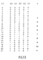
- Fig. 13 the relationship between the count CO and the number of bit cells is shown.
- Q1, Q2, Q3, Q4 and Q5 represent the bits of the count, Q1 denoting the least significant bit and Q5 the most significant bit. It is to be noted that the counts for which the least significant bit Q1 is "0", do not unambiguously indicate the number n.
- the bits Q1 ... Q5 representing the count CO are applied to a decoding circuit 128 which has three outputs for supplying a signal X0, X3 and X6.
- the signal X0 denotes that the count CO is equal to zero
- X3 denotes that the count CO is a read signal portion of V1' which is 3 bit cells in length
- X6 denotes that the count CO represents a read signal portion of V1' which is 6 bit cells in length.
- the decoding circuit 128 comprises a what is commonly referred to as inhibit input INH which inhibits the presentation of signals X0, X3 and X6.
- Input INH is supplied with a signal Z which is derived from the least significant bit Q1 at the output of the counter 123 and the signal T by means of AND gate 129 which has an inverting output.
- the output signal of the AND gate 129 is delayed by a delay circuit 130 over a brief period of time which is a fraction of the period of time T.
- the delayed signal at the output of the delay circuit 130 forms the signal Z.
- the signals X0, X3 and X6 at the output of the decoding circuit are derived in the following manner.
- AND gate 124 transfers the clock signal CK during the time interval Tt.
- the signal X3 is presented during the active period of the decoding circuit.
- the signal X6 is presented during the active period of the decoding circuit 128.
- the decoding circuit 128 Since the signal Z is applied via the delay circuit 130, the decoding circuit 128 is rendered inoperative one time interval after the counter 123 has been set to zero, which time interval corresponds to the delay period. During this time interval the signal X0 is generated.
- the signal X3 is generated for a brief period of time of about one clock period at the output of the decoding circuit. The generation of the signal X3 is immediately followed by a generation of the signal X0. The generation of the signals X3 and X0 is effected in a time interval in which the binary read signal V1' is "0". Similarly, in the case where the binary read signal V1' comprises 6 bit cells, the signal X6 and the signal X0 are successively generated in the time interval during which the binary read signal V1' is "0" again.
- Fig. 11 the part of the circuit shown in box 131 is used for determining the length deviation.
- the circuit comprises two AND gates 131 and 132 which have each their inverting and non-inverting input.
- the binary read signal V1' is applied to the non-inverting input of AND gate 132 and the inverting input of AND gate 133.
- the signal A delayed relative to signal V1' is applied to the inverting input of AND gate 132 and the non-inverting input of AND gate 133.
- the output signal of AND gate 132 adopts a "1" value at the beginning of each series of bit cells which have a logic "1" value in the binary read signal V1'.
- the difference of length between part 150 and part 151 denotes the extent of the length deviation.
- the circuit comprises a capacitor 134.
- a switch 136 controlled by the AND gate 132 connects the capacitor 134 to a current source 135 which current source charges capacitor 134 with a current I.
- a switch 138 controlled by the AND gate 133 connects a current source 137 to the capacitor which current source withdraws a current I from the capacitor.
- the consequential change of voltage across the capacitor 134 is a measure for the time difference Tb-Te and thus a measure for the length deviation.
- the capacitor 134 is connected through a switch 139 controlled by the signal X0 to a point of constant potential 140.
- the capacitor is further connected to a capacitor 142 through a switch 141 controlled by the signal X3, and to a capacitor 144 through a switch 143 controlled by the signal X6.
- the capacitance of the capacitors 142 and 144 is selected to be many times as large as the capacitance of the capacitor 134.
- the switch 139 is controlled by the signal X0, so that the capacitor voltage is made equal to the voltage of point 140. Then the length deviation of the next signal portion having the "1" value of the binary read signal V1' is measured by the capacitor 134. If there is detected that the length for which the length deviation is determined corresponds to three times the bit cell length, the switch 141 is closed under the influence of signal X3 and the capacitors 134 and 142 are temporarily connected in parallel.
- the voltage across the capacitor 144 will adopt a value which is a linear combination of the voltages across the capacitors 134 and 144 for the parallel combination. Since the capacitance of the capacitor 144 is selected to be many times as large as that of the capacitor 134, the voltage the capacitor 144 had prior to the inclusion in the parallel combination contributes considerably more to the voltage obtained from the parallel combination than the voltage the capacitor 134 had prior to the inclusion in the parallel combination. For that matter, the voltage across capacitor 144 will adopt a value corresponding to the average length deviation for the signal portions that correspond to 3 bit cells. The voltage across the capacitor 142 will adopt a value corresponding to the average length deviation for the signal portions that correspond to 6 bit cells.
- the quality signal Vm which represents the difference between the average length deviation shown by the voltage across capacitor 142 and the average length deviation shown by the voltage across capacitor 144 is determined by a differential amplifier 145.
- the length deviation is determined for the read signal portions that correspond to the length of 3 bit cells and that correspond to the length of 6 bit cells. It will be obvious that the average length deviation for read signal portions that correspond to the length of a different number of bit cells may be obtained similarly.
- Fig. 14 shows another implementation of the method according to the invention.
- This implementation relates to a reading device.
- Reference 160 denotes an optical read head of a customary type which produces a read signal V1.
- the read signal V1 is applied to an equalizing filter 161 which emphasizes the frequency components in the high-frequency region of the read signal spectrum.
- the frequencies to be emphasized are of the order of 1 MHz.
- Fig. 15 shows by way of illustration the frequency characteristic of an equalizing filter which is customarily used for reading a Compact Disc. The frequency corresponding to the I3 effects is approximately equal to 0.72 MHz.
- the read signal filtered by the equalizing filter 161 is converted into the binary read signal V1' by the detection circuit 19.
- the analysis circuit 20 derives the quality signal Vm from the signal V1'.
- the quality signal Vm denotes to what extent the length deviations of the read signal portions that correspond to short effects are different.
- the signal Vm is applied to a control circuit 162 for setting the extent to which the higher frequencies are emphasized by the equalizing filter 161.
- the extent to which the higher frequencies are emphasized is set to a value for which the quality signal Vm denotes that the length deviations of the read signal portions that correspond to the short effects are small.
- the adaptation of the equalizing filter can be realized by adapting the gain factor for the higher frequencies while maintaining the gain factor for lower frequencies.
- adaptation of the gain factor for the lower frequencies while maintaining the gain factors for the higher frequencies is alternatively possible. It is only essential that the ratio between the gain factors of the higher frequencies and those of the lower frequencies be adapted as a function of the quality signal.
Claims (11)
- Procédé pour former un signal de qualité se rapportant à un signal de lecture dérivé de points mémoire de longueur constante qui présentent une première ou une deuxième valeur, lequel signal de lecture est obtenu en lisant un modèle d'informations d'effets détectables par voie optique (32) qui représentent des groupes de points mémoire successifs qui présentent la première valeur logique, tandis que les premières parties de signal de lecture dépassant une valeur de référence dans une première direction correspondent aux effets dans le modèle d'informations lu de cette manière, et dans lequel le signal de qualité est dérivé sur la base des premières parties de signal de lecture,
ledit procédé étant caractérisé en ce que, lorsque le signal de qualité est dérivé, une première mesure est déterminée pour la différence de longueur entre la longueur réelle des premières parties de signal de lecture qui représentent des groupes de n points mémoire successifs et n fois la longueur de point mémoire, et dans lequel une valeur est sélectionnée pour n à laquelle la sensibilité de l'écart de longueur à certains changements de paramètres d'enregistrement (I) est relativement élevée par comparaison à la sensibilité d'autres premières parties de signal de lecture. - Procédé suivant la revendication 1, caractérisé en ce que, lorsque le signal de qualité est dérivé, une deuxième mesure est déterminée pour l'écart de longueur des parties de signal de lecture qui représentent des groupes de bits de m points mémoire successifs, le signal de qualité étant indicatif de la différence entre les première et deuxième mesures, une valeur étant sélectionnée pour m à laquelle la sensibilité de l'écart de longueur auxdits changements paramétriques est relativement faible par comparaison avec la sensibilité des écarts de longueur d'autres premières parties de signal de lecture.
- Procédé suivant la revendication 2, caractérisé en ce que n est égal à 3 et en ce que m est supérieur ou égal à 5 et inférieur ou égal à 7.
- Dispositif d'enregistrement pour enregistrer dans une couche d'enregistrement (3) un signal d'infonnation binaire comprenant des points mémoire de longueur constante, ces points mémoire ayant une première ou une deuxième valeur logique, le dispositif comprenant des moyens de balayage (18) pour balayer la couche d'enregistrement avec un faisceau de rayonnement, des moyens de modulation (6) pour moduler l'intensité du faisceau de rayonnement en réaction au signal d'information tandis qu'une certaine stratégie d'enregistrement est suivie, en conséquence de quoi un modèle d'informations d'effets détectables par voie optique est enregistré dans la couche d'enregistrement, lesdits effets représentant des groupes de points mémoire successifs ayant la première valeur logique, ledit dispositif comprenant en outre des moyens de lecture pour lire par voie optique le modèle d'informations pour lequel est produit un signal de lecture dans lequel des premières parties de signal de lecture dépassant une valeur de référence dans une première direction correspondent aux effets dans le modèle d'informations lu, des moyens d'analyse (20) pour analyser les premières parties de signal de lecture et pour produire un signal de qualité qui est indicatif du résultat de l'analyse effectuée, et des moyens d'adaptation pour adapter la stratégie d'enregistrement sur la base du signal de qualité, caractérisé en ce que les moyens d'analyse (20) comprennent des moyens de dérivation pour dériver une mesure pour l'écart de longueur entre la longueur réelle des premières parties de signal de lecture qui représentent des groupes de n points mémoire successifs et n fois la longueur de point mémoire, dans lequel le signal de qualité est indicatif de ladite mesure, dans lequel une valeur est sélectionnée pour n à laquelle la sensibilité de l'écart de longueur aux changements dans la stratégie d'enregistrement est relativement élevée par comparaison avec la sensibilité des écarts d'écriture d'autres premières parties de signal de lecture.
- Dispositif suivant la revendication 4, caractérisé en ce que les moyens d'analyse comprennent des moyens de détermination pour déterminer une deuxième mesure pour l'écart de longueur des premières parties de signal de lecture qui représentent des groupes de m points mémoire successifs, et des moyens de détermination pour déterminer la différence entre les première et deuxième mesures, le signal de qualité étant indicatif de ladite différence, une valeur étant sélectionnée pour m à laquelle la sensibilité de l'écart de longueur aux changements dans la stratégie d'enregistrement est relativement réduite par comparaison avec la sensibilité des écarts de longueur d'autres premières parties de signal de lecture.
- Dispositif suivant la revendication 5, caractérisé en ce que n est égal à 3 et en ce que m est supérieur ou égal à 5 et inférieur ou égal à 7.
- Dispositif suivant l'une des revendications 4 à 6, caractérisé en ce que les moyens de modulation (6) comprennent des moyens pour exécuter une stratégie d'enregistrement suivant laquelle l'intensité du faisceau de rayonnement est modulée de manière pulsée, et dans lequel les moyens d'adaptation sont conçus pour adapter l'intensité des impulsions de rayonnement dans un intervalle de temps situé un laps de temps prédéterminé après le début de chaque impulsion de rayonnement, le dispositif comprenant des moyens de réglage pour régler une valeur de référence à laquelle la longueur moyenne des premières parties de signal de lecture est, par essence, égale à la longueur moyenne des deuxièmes parties de signal de lecture qui sont situées entre les premières parties de signal de lecture dans le signal qui a été lu.
- Dispositif suivant la revendication 7, caractérisé en ce que le dispositif comprend des moyens de détection pour détecter le rayonnement réfléchi par la couche d'enregistrement au cours de l'enregistrement, et des moyens de réglage pour régler le niveau d'intensité adopté par le faisceau de rayonnement au cours du laps de temps au début de chaque impulsion de rayonnement en fonction du comportement de l'intensité du rayonnement réfléchi au cours desdits intervalles au début des impulsions de rayonnement.
- Dispositif de lecture pour lire un modèle d'informations d'une couche d'enregistrement, lequel modèle d'informations représente un signal d'information binaire comprenant des points mémoire de longueur constante, lesquels points mémoire présentent une première ou deuxième valeur logique, le modèle d'informations comprenant des effets détectables par voie optique qui représentent des groupes de points mémoire successifs ayant la première valeur logique, le dispositif comprenant des moyens de lecture (60) pour lire par voie optique le modèle d'informations, moyens de lecture dans lesquels un signal est lu dont les premières parties de signal de lecture dépassant une valeur de référence dans une première direction correspondent aux effets dans le signal d'informations lu, caractérisé en ce que des moyens de filtre (61) sont prévus pour filtrer le signal de lecture, moyens de filtre dans lesquels le rapport entre le facteur de gain des parties de signal de lecture dans une gamme de fréquences spécifique et des parties de signal de lecture en dehors de cette gamme de fréquences peut être réglé, des moyens d'analyse (20) pour déterminer un signal de qualité qui est une mesure de l'écart de longueur entre les longueurs réelles des premières parties de signal de lecture qui représentent des groupes de n points mémoire successifs et n fois la longueur de point mémoire, et des moyens d'adaptation (16) pour adapter ledit rapport entre les facteurs de gain en fonction du signal de qualité, une valeur étant sélectionnée pour n à laquelle la fréquence des parties de signal de lecture de n fois la longueur de point mémoire se trouve dans ladite gamme de fréquences.
- Dispositif suivant la revendication 9, caractérisé en ce que les moyens d'analyse (20) comprennent des moyens de détermination pour déterminer une deuxième mesure de l'écart de longueur des premières parties de signal de lecture qui représentent des groupes de bits de m points mémoire successifs, et des moyens de détermination pour déterminer la différence entre les première et deuxième mesures, le signal de qualité étant indicatif de ladite différence, une valeur étant sélectionnée pour m à laquelle la fréquence des parties de signal de lecture de m fois la longueur de point mémoire se trouve en dehors de ladite gamme de fréquences.
- Dispositif suivant la revendication 10, caractérisé en ce que n est égal à 3 et en ce que m est supérieur ou égal à 5 et inférieur ou égal à 7.
Applications Claiming Priority (2)
| Application Number | Priority Date | Filing Date | Title |
|---|---|---|---|
| BE9300398A BE1007029A3 (nl) | 1993-04-22 | 1993-04-22 | Werkwijze voor het afleiden van een kwaliteitssignaal uit een uitgelezen signaal, alsmede een optekeninrichting en een uitleesinrichting waarin een dergelijke werkwijze wordt toegepast. |
| BE9300398 | 1993-04-22 |
Publications (2)
| Publication Number | Publication Date |
|---|---|
| EP0621589A1 EP0621589A1 (fr) | 1994-10-26 |
| EP0621589B1 true EP0621589B1 (fr) | 1999-06-09 |
Family
ID=3886992
Family Applications (1)
| Application Number | Title | Priority Date | Filing Date |
|---|---|---|---|
| EP94201023A Expired - Lifetime EP0621589B1 (fr) | 1993-04-22 | 1994-03-14 | Méthode pour obtenir un signal "qualité" d'un signal lu, ainsi qu'un dispositif d'enregistrement et un dispositif de lecture utilisant une telle méthode |
Country Status (6)
| Country | Link |
|---|---|
| US (1) | US5587980A (fr) |
| EP (1) | EP0621589B1 (fr) |
| JP (1) | JP3555981B2 (fr) |
| BE (1) | BE1007029A3 (fr) |
| DE (1) | DE69418934T2 (fr) |
| TW (1) | TW228588B (fr) |
Families Citing this family (11)
| Publication number | Priority date | Publication date | Assignee | Title |
|---|---|---|---|---|
| US5894468A (en) * | 1994-05-06 | 1999-04-13 | Discovision Associates | Data recovery with differentiation and partial integration stages to eliminate noises and DC offset level |
| US5696756A (en) * | 1995-04-14 | 1997-12-09 | Kabushiki Kaishia Toshiba | Optical disk having an evaluation pattern for evaluating the optical disk |
| EP1064649B1 (fr) | 1998-02-27 | 2012-04-25 | Doug Carson & Associates, Inc. | Reglage individuel de positions de transition entre sommets et creux dans un systeme de matri age de disque optique |
| US5986495A (en) * | 1998-03-17 | 1999-11-16 | Chen; Wen-Pin | Key switch control device |
| JP2002117542A (ja) * | 2000-10-05 | 2002-04-19 | Pioneer Electronic Corp | 多層回転記録媒体及びその記録再生方法並びに記録再生装置 |
| TWI242194B (en) * | 2001-09-26 | 2005-10-21 | Sony Corp | Parallel/serial conversion circuit, light output control circuit, and optical recording apparatus |
| US7038982B2 (en) * | 2001-09-27 | 2006-05-02 | Koninklijke Philips Electronics N.V. | Method and recording device for selecting an optimized write strategy and recording medium for use by the method |
| US7477584B2 (en) * | 2003-11-11 | 2009-01-13 | Samsung Electronics Co., Ltd. | Recording and/or reproducing apparatus and method with a signal quality determining device and method |
| CN1622206A (zh) * | 2003-11-26 | 2005-06-01 | 皇家飞利浦电子股份有限公司 | 一种光盘刻写参数的优化方法及装置 |
| EP1736984A1 (fr) * | 2005-06-24 | 2006-12-27 | Deutsche Thomson-Brandt Gmbh | Procédé pour déterminer automatiquement une stratégie d'écriture |
| JP4523583B2 (ja) * | 2006-12-27 | 2010-08-11 | 太陽誘電株式会社 | データ記録評価方法及び光ディスク記録再生装置 |
Family Cites Families (23)
| Publication number | Priority date | Publication date | Assignee | Title |
|---|---|---|---|---|
| JPS54143109A (en) * | 1978-04-28 | 1979-11-08 | Hitachi Ltd | Optical information device |
| NL8105095A (nl) * | 1981-11-11 | 1983-06-01 | Philips Nv | Schakeling voor het omzetten van een informatiesignaal in een rechthoekvormig signaal. |
| US4688204A (en) * | 1984-11-16 | 1987-08-18 | Storage Technology Partners Ii | Pulsed optical data detection system |
| US4646103A (en) * | 1985-03-20 | 1987-02-24 | Hitachi, Ltd. | Optical recording method |
| JP2810035B2 (ja) * | 1986-08-22 | 1998-10-15 | 株式会社日立製作所 | 光学的記録再生方法 |
| NL8602718A (nl) * | 1986-10-29 | 1988-05-16 | Philips Nv | Werkwijze voor het optekenen van een tweewaardig signaal op een optisch uitleesbare registratiedrager en een inrichting voor het uitvoeren van de werkwijze. |
| NL8800223A (nl) * | 1987-04-21 | 1988-11-16 | Philips Nv | Systeem voor het registreren van een informatiesignaal, alsmede een registratiedrager en registratieinrichting voor toepassing in het systeem. |
| JP2684657B2 (ja) * | 1987-11-13 | 1997-12-03 | ヤマハ株式会社 | 光ディスク記録方法 |
| JPH01229516A (ja) * | 1988-03-10 | 1989-09-13 | Sony Corp | 自動等化器 |
| JPH02162529A (ja) * | 1988-12-15 | 1990-06-22 | Pioneer Electron Corp | 光学式記録装置及び光ディスク |
| NL9000328A (nl) * | 1989-06-23 | 1991-01-16 | Philips Nv | Werkwijze en inrichting voor het aanbrengen van informatiepatronen op een registratiedrager. |
| JP2708859B2 (ja) * | 1989-03-16 | 1998-02-04 | 三洋電機株式会社 | 光ディスク記録装置 |
| JPH0810490B2 (ja) * | 1989-03-20 | 1996-01-31 | 富士通株式会社 | 光ディスク情報書込制御方法およびその装置 |
| US5303217A (en) * | 1989-06-23 | 1994-04-12 | U.S. Philips Corporation | Optical recording device wherein recording beam intensity is set in accordance with an optimum value of the DC component of a recorded signal |
| ATE114856T1 (de) * | 1989-06-23 | 1994-12-15 | Philips Nv | Aufzeichnungsanordnung zum anbringen eines informationsmusters auf einem strahlungsempfindlichen aufzeichnungsträger. |
| US5128921A (en) * | 1989-09-28 | 1992-07-07 | Tandy Corporation | Method and apparatus for pre-compensation in an optical disc |
| US5043971A (en) * | 1989-09-28 | 1991-08-27 | Tandy Corporation | Method and apparatus for pre-compensation in an optical disc |
| JP2797733B2 (ja) * | 1990-03-14 | 1998-09-17 | 松下電器産業株式会社 | 光学情報記録部材の記録方法 |
| EP0910069A3 (fr) * | 1990-05-25 | 2008-04-16 | Hitachi, Ltd. | Disque optique |
| US5418770A (en) * | 1990-06-29 | 1995-05-23 | Hitachi, Ltd. | Method of and apparatus for correcting edge interval of pit in optical recording/read-out apparatus |
| US5241524A (en) * | 1990-08-29 | 1993-08-31 | Olympus Optical Co., Ltd. | Method of edge recording on optical record medium |
| JP2556725Y2 (ja) * | 1991-01-30 | 1997-12-08 | 株式会社ケンウッド | シンメトリ装置 |
| JP3039056B2 (ja) * | 1991-11-25 | 2000-05-08 | ソニー株式会社 | 追記型光ディスク記録装置 |
-
1993
- 1993-04-22 BE BE9300398A patent/BE1007029A3/nl not_active IP Right Cessation
-
1994
- 1994-03-14 DE DE69418934T patent/DE69418934T2/de not_active Expired - Fee Related
- 1994-03-14 EP EP94201023A patent/EP0621589B1/fr not_active Expired - Lifetime
- 1994-03-21 TW TW083102464A patent/TW228588B/zh active
- 1994-03-29 US US08/219,321 patent/US5587980A/en not_active Expired - Lifetime
- 1994-04-19 JP JP08050594A patent/JP3555981B2/ja not_active Expired - Fee Related
Also Published As
| Publication number | Publication date |
|---|---|
| EP0621589A1 (fr) | 1994-10-26 |
| TW228588B (en) | 1994-08-21 |
| DE69418934T2 (de) | 1999-12-16 |
| DE69418934D1 (de) | 1999-07-15 |
| JP3555981B2 (ja) | 2004-08-18 |
| BE1007029A3 (nl) | 1995-02-21 |
| US5587980A (en) | 1996-12-24 |
| JPH06333235A (ja) | 1994-12-02 |
Similar Documents
| Publication | Publication Date | Title |
|---|---|---|
| KR940001446B1 (ko) | 정보기록 재생방법 및 장치 | |
| CA1194230A (fr) | Systeme de controle pour appareil d'enregistrement de donnees optique | |
| US5233589A (en) | Method for recording/reproducing information having a function of correcting variations in the interval in reproduced data and apparatus for realizing same | |
| EP0793221B1 (fr) | Méthode et dispositif d'enregistrement optique | |
| CN1117358C (zh) | 用于写入光学记录载体的方法和装置 | |
| US5345434A (en) | Method and apparatus for correcting edge interval of record signal in an optical record/read-out apparatus | |
| EP0418070B1 (fr) | Appareil pour l'enregistrement et la reproduction des informations | |
| US5631891A (en) | Disk reproducing circuit with automatic gain control | |
| EP0621589B1 (fr) | Méthode pour obtenir un signal "qualité" d'un signal lu, ainsi qu'un dispositif d'enregistrement et un dispositif de lecture utilisant une telle méthode | |
| US4811316A (en) | Apparatus for seeking a track of an optical information carrier in which a loss of detection signal is compensated for | |
| JPH07169064A (ja) | マルチビーム記録再生装置 | |
| JPS60109035A (ja) | 光学記録担体再生装置 | |
| US5661713A (en) | Optical information reproducing apparatus with a threshold level generator to eliminate DC level fluctuation | |
| EP0606478A1 (fr) | Appareil de restitution de donnees | |
| US4672596A (en) | Level controlled readout system for formatted record recorded on an optical disc | |
| US4525822A (en) | Optical data recordation and reproduction system | |
| NL8702904A (nl) | Werkwijze en inrichting voor het optekenen van informatie op een registratiedrager, alsmede een inrichting voor het lezen van de opgetekende informatie. | |
| EP0219037B1 (fr) | Circuit de traitement d'une forme d'onde | |
| US6181659B1 (en) | Optical information recording method for optical information recording apparatus | |
| JP2594948B2 (ja) | 信号記録再生装置及び信号記録再生方法 | |
| JPS61134928A (ja) | 記録/未記録信号判定回路 | |
| NL193156C (nl) | Reproductieketen voor gegevens van een optische schijf. | |
| US5181196A (en) | Erase mark detecting circuit for detecting an erase mark superimposed on data recorded on a sector of an optical recording medium | |
| JPH06180950A (ja) | 光学的情報再生装置 | |
| JPH0528503A (ja) | 光記録再生装置 |
Legal Events
| Date | Code | Title | Description |
|---|---|---|---|
| PUAI | Public reference made under article 153(3) epc to a published international application that has entered the european phase |
Free format text: ORIGINAL CODE: 0009012 |
|
| AK | Designated contracting states |
Kind code of ref document: A1 Designated state(s): DE FR GB |
|
| 17P | Request for examination filed |
Effective date: 19950426 |
|
| 17Q | First examination report despatched |
Effective date: 19970722 |
|
| GRAG | Despatch of communication of intention to grant |
Free format text: ORIGINAL CODE: EPIDOS AGRA |
|
| RAP3 | Party data changed (applicant data changed or rights of an application transferred) |
Owner name: KONINKLIJKE PHILIPS ELECTRONICS N.V. |
|
| GRAG | Despatch of communication of intention to grant |
Free format text: ORIGINAL CODE: EPIDOS AGRA |
|
| GRAH | Despatch of communication of intention to grant a patent |
Free format text: ORIGINAL CODE: EPIDOS IGRA |
|
| GRAH | Despatch of communication of intention to grant a patent |
Free format text: ORIGINAL CODE: EPIDOS IGRA |
|
| GRAA | (expected) grant |
Free format text: ORIGINAL CODE: 0009210 |
|
| AK | Designated contracting states |
Kind code of ref document: B1 Designated state(s): DE FR GB |
|
| REF | Corresponds to: |
Ref document number: 69418934 Country of ref document: DE Date of ref document: 19990715 |
|
| ET | Fr: translation filed | ||
| PLBE | No opposition filed within time limit |
Free format text: ORIGINAL CODE: 0009261 |
|
| STAA | Information on the status of an ep patent application or granted ep patent |
Free format text: STATUS: NO OPPOSITION FILED WITHIN TIME LIMIT |
|
| 26N | No opposition filed | ||
| REG | Reference to a national code |
Ref country code: GB Ref legal event code: IF02 |
|
| PGFP | Annual fee paid to national office [announced via postgrant information from national office to epo] |
Ref country code: DE Payment date: 20080515 Year of fee payment: 15 |
|
| PGFP | Annual fee paid to national office [announced via postgrant information from national office to epo] |
Ref country code: FR Payment date: 20080327 Year of fee payment: 15 |
|
| PGFP | Annual fee paid to national office [announced via postgrant information from national office to epo] |
Ref country code: GB Payment date: 20080425 Year of fee payment: 15 |
|
| GBPC | Gb: european patent ceased through non-payment of renewal fee |
Effective date: 20090314 |
|
| REG | Reference to a national code |
Ref country code: FR Ref legal event code: ST Effective date: 20091130 |
|
| PG25 | Lapsed in a contracting state [announced via postgrant information from national office to epo] |
Ref country code: DE Free format text: LAPSE BECAUSE OF NON-PAYMENT OF DUE FEES Effective date: 20091001 |
|
| PG25 | Lapsed in a contracting state [announced via postgrant information from national office to epo] |
Ref country code: GB Free format text: LAPSE BECAUSE OF NON-PAYMENT OF DUE FEES Effective date: 20090314 Ref country code: FR Free format text: LAPSE BECAUSE OF NON-PAYMENT OF DUE FEES Effective date: 20091123 |