EP0618627A1 - Zusammengesetzter supraleitender Draht und Verfahren zu seiner Herstellung - Google Patents
Zusammengesetzter supraleitender Draht und Verfahren zu seiner Herstellung Download PDFInfo
- Publication number
- EP0618627A1 EP0618627A1 EP93120670A EP93120670A EP0618627A1 EP 0618627 A1 EP0618627 A1 EP 0618627A1 EP 93120670 A EP93120670 A EP 93120670A EP 93120670 A EP93120670 A EP 93120670A EP 0618627 A1 EP0618627 A1 EP 0618627A1
- Authority
- EP
- European Patent Office
- Prior art keywords
- base metal
- metal material
- superconducting wire
- filaments
- composite
- Prior art date
- Legal status (The legal status is an assumption and is not a legal conclusion. Google has not performed a legal analysis and makes no representation as to the accuracy of the status listed.)
- Granted
Links
- 150000001875 compounds Chemical class 0.000 title claims abstract description 45
- 238000000034 method Methods 0.000 title claims description 40
- 238000004519 manufacturing process Methods 0.000 title claims description 22
- 239000010953 base metal Substances 0.000 claims abstract description 282
- 239000010949 copper Substances 0.000 claims abstract description 221
- 239000002131 composite material Substances 0.000 claims abstract description 182
- 239000000463 material Substances 0.000 claims abstract description 179
- 239000002243 precursor Substances 0.000 claims abstract description 138
- KUNSUQLRTQLHQQ-UHFFFAOYSA-N copper tin Chemical compound [Cu].[Sn] KUNSUQLRTQLHQQ-UHFFFAOYSA-N 0.000 claims abstract description 105
- 229910000657 niobium-tin Inorganic materials 0.000 claims abstract description 103
- 229910000906 Bronze Inorganic materials 0.000 claims abstract description 86
- 239000010974 bronze Substances 0.000 claims abstract description 86
- 239000011159 matrix material Substances 0.000 claims abstract description 29
- 229910052718 tin Inorganic materials 0.000 claims abstract description 21
- 229910045601 alloy Inorganic materials 0.000 claims abstract description 17
- 239000000956 alloy Substances 0.000 claims abstract description 17
- 229910052733 gallium Inorganic materials 0.000 claims abstract description 17
- 229910000999 vanadium-gallium Inorganic materials 0.000 claims abstract description 5
- 230000004888 barrier function Effects 0.000 claims description 30
- 229910052719 titanium Inorganic materials 0.000 claims description 26
- 230000000087 stabilizing effect Effects 0.000 claims description 20
- 229910052715 tantalum Inorganic materials 0.000 claims description 20
- 229910052720 vanadium Inorganic materials 0.000 claims description 16
- 229910052732 germanium Inorganic materials 0.000 claims description 15
- 229910052738 indium Inorganic materials 0.000 claims description 15
- 229910052748 manganese Inorganic materials 0.000 claims description 15
- 229910052710 silicon Inorganic materials 0.000 claims description 15
- 229910052735 hafnium Inorganic materials 0.000 claims description 11
- 229910052726 zirconium Inorganic materials 0.000 claims description 11
- 229910052750 molybdenum Inorganic materials 0.000 claims description 8
- 238000005096 rolling process Methods 0.000 claims description 7
- 238000006243 chemical reaction Methods 0.000 claims description 5
- 238000005553 drilling Methods 0.000 claims description 3
- 238000007747 plating Methods 0.000 claims description 2
- 238000010438 heat treatment Methods 0.000 abstract description 68
- 238000009792 diffusion process Methods 0.000 abstract description 51
- 230000003247 decreasing effect Effects 0.000 abstract description 23
- 229910052802 copper Inorganic materials 0.000 description 33
- RYGMFSIKBFXOCR-UHFFFAOYSA-N Copper Chemical compound [Cu] RYGMFSIKBFXOCR-UHFFFAOYSA-N 0.000 description 24
- 229910017755 Cu-Sn Inorganic materials 0.000 description 19
- 229910017927 Cu—Sn Inorganic materials 0.000 description 19
- 238000001125 extrusion Methods 0.000 description 16
- 239000000203 mixture Substances 0.000 description 16
- 230000006641 stabilisation Effects 0.000 description 14
- 238000011105 stabilization Methods 0.000 description 14
- 239000001307 helium Substances 0.000 description 13
- 229910052734 helium Inorganic materials 0.000 description 13
- SWQJXJOGLNCZEY-UHFFFAOYSA-N helium atom Chemical compound [He] SWQJXJOGLNCZEY-UHFFFAOYSA-N 0.000 description 13
- 239000007788 liquid Substances 0.000 description 13
- 239000002887 superconductor Substances 0.000 description 13
- 238000005259 measurement Methods 0.000 description 12
- 239000002184 metal Substances 0.000 description 12
- 229910052751 metal Inorganic materials 0.000 description 12
- 229910052758 niobium Inorganic materials 0.000 description 12
- 238000000886 hydrostatic extrusion Methods 0.000 description 10
- 238000010894 electron beam technology Methods 0.000 description 9
- 230000009467 reduction Effects 0.000 description 9
- 238000003466 welding Methods 0.000 description 9
- 230000000694 effects Effects 0.000 description 8
- 239000011573 trace mineral Substances 0.000 description 7
- 235000013619 trace mineral Nutrition 0.000 description 7
- 230000008878 coupling Effects 0.000 description 6
- 238000010168 coupling process Methods 0.000 description 6
- 238000005859 coupling reaction Methods 0.000 description 6
- 230000008569 process Effects 0.000 description 5
- 150000002739 metals Chemical class 0.000 description 3
- 229910001128 Sn alloy Inorganic materials 0.000 description 2
- 229910052782 aluminium Inorganic materials 0.000 description 2
- 230000015572 biosynthetic process Effects 0.000 description 2
- 238000005520 cutting process Methods 0.000 description 2
- 239000004615 ingredient Substances 0.000 description 2
- 229910000765 intermetallic Inorganic materials 0.000 description 2
- 230000002093 peripheral effect Effects 0.000 description 2
- 239000000843 powder Substances 0.000 description 2
- 238000012545 processing Methods 0.000 description 2
- 229910018082 Cu3Sn Inorganic materials 0.000 description 1
- 229910001257 Nb alloy Inorganic materials 0.000 description 1
- 229910020888 Sn-Cu Inorganic materials 0.000 description 1
- 229910019204 Sn—Cu Inorganic materials 0.000 description 1
- ATJFFYVFTNAWJD-UHFFFAOYSA-N Tin Chemical compound [Sn] ATJFFYVFTNAWJD-UHFFFAOYSA-N 0.000 description 1
- 239000000654 additive Substances 0.000 description 1
- 230000000996 additive effect Effects 0.000 description 1
- QVGXLLKOCUKJST-UHFFFAOYSA-N atomic oxygen Chemical compound [O] QVGXLLKOCUKJST-UHFFFAOYSA-N 0.000 description 1
- 230000000903 blocking effect Effects 0.000 description 1
- 230000015556 catabolic process Effects 0.000 description 1
- 238000007796 conventional method Methods 0.000 description 1
- 238000001816 cooling Methods 0.000 description 1
- 238000006731 degradation reaction Methods 0.000 description 1
- 238000013461 design Methods 0.000 description 1
- 230000006866 deterioration Effects 0.000 description 1
- 239000006185 dispersion Substances 0.000 description 1
- 230000006872 improvement Effects 0.000 description 1
- 238000003780 insertion Methods 0.000 description 1
- 230000037431 insertion Effects 0.000 description 1
- 230000005415 magnetization Effects 0.000 description 1
- 238000000465 moulding Methods 0.000 description 1
- 229910052759 nickel Inorganic materials 0.000 description 1
- 238000009828 non-uniform distribution Methods 0.000 description 1
- 230000003287 optical effect Effects 0.000 description 1
- 239000001301 oxygen Substances 0.000 description 1
- 229910052760 oxygen Inorganic materials 0.000 description 1
- 238000002360 preparation method Methods 0.000 description 1
- 238000009877 rendering Methods 0.000 description 1
- 238000007669 thermal treatment Methods 0.000 description 1
- 238000011282 treatment Methods 0.000 description 1
- 238000004804 winding Methods 0.000 description 1
Images


Classifications
-
- H—ELECTRICITY
- H10—SEMICONDUCTOR DEVICES; ELECTRIC SOLID-STATE DEVICES NOT OTHERWISE PROVIDED FOR
- H10N—ELECTRIC SOLID-STATE DEVICES NOT OTHERWISE PROVIDED FOR
- H10N60/00—Superconducting devices
- H10N60/01—Manufacture or treatment
- H10N60/0184—Manufacture or treatment of devices comprising intermetallic compounds of type A-15, e.g. Nb3Sn
-
- Y—GENERAL TAGGING OF NEW TECHNOLOGICAL DEVELOPMENTS; GENERAL TAGGING OF CROSS-SECTIONAL TECHNOLOGIES SPANNING OVER SEVERAL SECTIONS OF THE IPC; TECHNICAL SUBJECTS COVERED BY FORMER USPC CROSS-REFERENCE ART COLLECTIONS [XRACs] AND DIGESTS
- Y10—TECHNICAL SUBJECTS COVERED BY FORMER USPC
- Y10S—TECHNICAL SUBJECTS COVERED BY FORMER USPC CROSS-REFERENCE ART COLLECTIONS [XRACs] AND DIGESTS
- Y10S505/00—Superconductor technology: apparatus, material, process
- Y10S505/80—Material per se process of making same
- Y10S505/812—Stock
-
- Y—GENERAL TAGGING OF NEW TECHNOLOGICAL DEVELOPMENTS; GENERAL TAGGING OF CROSS-SECTIONAL TECHNOLOGIES SPANNING OVER SEVERAL SECTIONS OF THE IPC; TECHNICAL SUBJECTS COVERED BY FORMER USPC CROSS-REFERENCE ART COLLECTIONS [XRACs] AND DIGESTS
- Y10—TECHNICAL SUBJECTS COVERED BY FORMER USPC
- Y10S—TECHNICAL SUBJECTS COVERED BY FORMER USPC CROSS-REFERENCE ART COLLECTIONS [XRACs] AND DIGESTS
- Y10S505/00—Superconductor technology: apparatus, material, process
- Y10S505/80—Material per se process of making same
- Y10S505/815—Process of making per se
- Y10S505/818—Coating
- Y10S505/821—Wire
-
- Y—GENERAL TAGGING OF NEW TECHNOLOGICAL DEVELOPMENTS; GENERAL TAGGING OF CROSS-SECTIONAL TECHNOLOGIES SPANNING OVER SEVERAL SECTIONS OF THE IPC; TECHNICAL SUBJECTS COVERED BY FORMER USPC CROSS-REFERENCE ART COLLECTIONS [XRACs] AND DIGESTS
- Y10—TECHNICAL SUBJECTS COVERED BY FORMER USPC
- Y10S—TECHNICAL SUBJECTS COVERED BY FORMER USPC CROSS-REFERENCE ART COLLECTIONS [XRACs] AND DIGESTS
- Y10S505/00—Superconductor technology: apparatus, material, process
- Y10S505/825—Apparatus per se, device per se, or process of making or operating same
- Y10S505/884—Conductor
-
- Y—GENERAL TAGGING OF NEW TECHNOLOGICAL DEVELOPMENTS; GENERAL TAGGING OF CROSS-SECTIONAL TECHNOLOGIES SPANNING OVER SEVERAL SECTIONS OF THE IPC; TECHNICAL SUBJECTS COVERED BY FORMER USPC CROSS-REFERENCE ART COLLECTIONS [XRACs] AND DIGESTS
- Y10—TECHNICAL SUBJECTS COVERED BY FORMER USPC
- Y10T—TECHNICAL SUBJECTS COVERED BY FORMER US CLASSIFICATION
- Y10T29/00—Metal working
- Y10T29/49—Method of mechanical manufacture
- Y10T29/49002—Electrical device making
- Y10T29/49014—Superconductor
-
- Y—GENERAL TAGGING OF NEW TECHNOLOGICAL DEVELOPMENTS; GENERAL TAGGING OF CROSS-SECTIONAL TECHNOLOGIES SPANNING OVER SEVERAL SECTIONS OF THE IPC; TECHNICAL SUBJECTS COVERED BY FORMER USPC CROSS-REFERENCE ART COLLECTIONS [XRACs] AND DIGESTS
- Y10—TECHNICAL SUBJECTS COVERED BY FORMER USPC
- Y10T—TECHNICAL SUBJECTS COVERED BY FORMER US CLASSIFICATION
- Y10T428/00—Stock material or miscellaneous articles
- Y10T428/12—All metal or with adjacent metals
- Y10T428/12431—Foil or filament smaller than 6 mils
- Y10T428/12438—Composite
-
- Y—GENERAL TAGGING OF NEW TECHNOLOGICAL DEVELOPMENTS; GENERAL TAGGING OF CROSS-SECTIONAL TECHNOLOGIES SPANNING OVER SEVERAL SECTIONS OF THE IPC; TECHNICAL SUBJECTS COVERED BY FORMER USPC CROSS-REFERENCE ART COLLECTIONS [XRACs] AND DIGESTS
- Y10—TECHNICAL SUBJECTS COVERED BY FORMER USPC
- Y10T—TECHNICAL SUBJECTS COVERED BY FORMER US CLASSIFICATION
- Y10T428/00—Stock material or miscellaneous articles
- Y10T428/12—All metal or with adjacent metals
- Y10T428/12486—Laterally noncoextensive components [e.g., embedded, etc.]
Definitions
- the present invention relates to a compound superconducting wire suitable for use in superconducting magnets of high magnetic field and a method for manufacturing the same.
- the present invention is advantageously applicable to an Nb-Sn compound superconducting wire and a manufacturing method therefor.
- the conventional method for manufacturing an Nb3Sn superconducting wire using the internal diffusion method is as follows. First, an Nb base metal material is inserted into a Cu tube and processed to decrease the area in section to a certain diameter thereby giving a single core wire. This single core wire is cut into pieces having an appropriate length and a plurality of these wire pieces are stuffed into a container made of Cu. In the center portion of this container is disposed a Cu base metal material such as a Cu rod or a bundle of Cu wires. Air in the container is evacuated, a cover is welded to the container to seal it up, and the thus treated container is extruded. Thereafter the Cu base metal material in the center portion of the container is mechanically formed with an aperture.
- An Sn base metal material is inserted into this aperture, and the Cu container is circumferentially covered with a tube made of Ta or Nb, which is further covered with a Cu tube.
- the resultant is processed to reduce the cross-sectional area, typically is drawn to a small size.
- a plurality of the thus obtained composite wires may be inserted into a Cu tube and then drawn to reduce the section area. After drawing the wire to a final diameter, it is twisted and subjected to a heat treatment. This heat treatment causes Sn to diffuse into Cu existing therearound to form Cu-Sn alloy and further to react with the Nb base metal filament to produce Nb3Sn either partially or entirely.
- the superconducting wire precursor in the aforesaid internal diffusion method has a structure in which the Nb base metal filaments and a core of the Sn base metal material are embedded in the Cu base metal material.
- the critical current density (Jc) which is one of the characteristics of superconductivity
- the Nb base metal filaments are embedded in the Cu base metal material as tightly as possible.
- the superconducting wire when cooled to the temperature of liquid helium is capable of allowing heavy current to flow therein without producing any electrical resistance.
- the Sn base metal material is disposed at the center of the module and, hence, the space between adjacent Nb3Sn filaments is as narrow as about a half of the spacing between such filaments arranged in accordance with a usual bronze method.
- the Nb base metal filaments tend to come into contact with each other to combine to each other when the superconducting wire precursor is heat-treated, thus resulting in increase of the effective filament diameter (d eff ), which greatly influences the electrical characteristics of the superconducting wire.
- the present inventors have found that the phenomenon that Nb3Sn filaments of a superconducting wire come into mutual contact, as encountered in heat-treating the precursor wire, appears particularly in an ⁇ -phase boundary (outer periphery of ⁇ -phase bronze layer) region, namely a region having a certain width in the radial direction in which the boundary of the ⁇ -phase bronze locates, and the above objects can be achieved by preventing the Nb3Sn filaments from contacting each other in this region.
- ⁇ -phase boundary outer periphery of ⁇ -phase bronze layer
- the bronze matrix comprises an outer low Sn concentration bronze region, an inner low Sn concentration bronze region, and an annular ⁇ -phase bronze boundary region which is located between the outer and inner regions and in which the boundary of the ⁇ -phase bronze produced at a temperature of 300° to 600°C and converted into ⁇ -phase bronze at a higher temperature appears and the Nb3Sn superconductor filaments are arranged with a larger spacing as compared to the arrangement in the other matrix regions.
- the mutual contact of the Nb3Sn filaments which is considered owing to expansion, movement or swaying of filaments during the heat treatment of the precursor wire can also be decreased by not arranging the filaments in the inside of the boundary of the ⁇ -phase bronze layer. Accordingly, even if the spacing between the any adjacent filaments arranged in the boundary region of the ⁇ -phase bronze layer is not increased, it is possible to provide an improved Nb3Sn superconducting wire by arranging the Nb3Sn filaments in the same manner as in a conventional internal diffusion method except that the filaments are not arranged in the inside of the boundary of the ⁇ -phase bronze layer.
- This technique is also advantageously applicable to the preparation of other compound type superconducting wires, e.g., V3Ga, Nb3Al and V3Si.
- a compound superconducting wire precursor comprising a composite composed of a Cu base metal material and a first base metal material X capable of forming an alloy with the Cu base metal material, and a multiplicity of filaments of a second base metal material Z which are provided within the composite so as not to come into mutual contact.
- the compound superconducting wire according to the second aspect of the present invention is obtained by heat-treating the aforesaid superconducting wire precursor, and thereby converting the filaments of the second base metal material Z into Z3X filaments and forming a Cu-X alloy as the matrix for the Z3X filaments.
- the first base metal material X such as Sn or Ga
- the area capable of being provided with filaments is increased by the area of the central portion.
- This makes it possible to enlarge the spacing between adjacent filaments by about 30 % as compared with that according to a conventional internal diffusion method. Consequently there is achieved a remarkable reduction in the probability of mutual contact between superconducting filaments in the superconducting wire obtained by the heat treatment of the precursor, resulting in a substantial reduction in the effective filament diameter value.
- the distance of diffusion of the first base metal X such as Sn or Ga is shortened to assure a uniform content of Sn or Ga after the diffusion.
- the composition of the Nb3Sn filaments or the like to be produced is made homogeneous thereby improving the n value which is one of the characteristics of superconductivity.
- the preheating time required for diffusion of the first base metal X can be shortened, which leads to a reduction in cost.
- Nb and Sn can be replaced with other metals Z and X, for example, V and Ga, respectively, and that a superconducting wire using a compound other than Nb3Sn produces substantially the same effects as a superconducting wire using Nb3Sn.
- V3Ga is particularly practical.
- the expression like “A base metal" or “base metal material A” is employed because the metal A as a base metal may form an alloy or an intermetallic compound in combination with another metal.
- the Nb-Sn superconducting wire according to the first aspect of the present invention has Nb3Sn filaments embedded in a bronze layer with such a space between adjacent filaments as not to cause their mutual contact or coupling.
- the precursor is prepared in such a manner that the space between adjacent Nb base metal filaments is made larger in a region in which Nb base metal filaments are easy to come into contact with each other in the heat treatment step, namely a boundary region of an ⁇ -phase bronze layer produced when preheated at a temperature of 300° to 600°C, than in other regions.
- the superconducting wire precursor having such an arrangement of the Nb filaments is heat-treated.
- the preheating is performed, before the heat treatment for turning the superconducting wire precursor into a superconducting wire, at a temperature of 300° to 600°C for diffusing an Sn base metal material located in the center portion of the precursor into a surrounding Cu base metal material to form a bronze matrix of a Cu-Sn alloy.
- the preheating is followed by the heat treatment.
- the ⁇ -phase bronze layer is one of the phases of Cu-Sn alloy produced in a heating temperature range of 300° to 600°C upon the heat treatment for causing the centrally-located Sn base metal material to diffuse into the Cu base metal material to form bronze, and means an intermetallic compound represented by Cu3Sn.
- the ⁇ -phase bronze is rigid and brittle as compared with ⁇ -phase bronze. In the heat treatment at a temperature of 600° to 800°C , the ⁇ -phase once produced disappears because of creation of Nb3Sn. The ⁇ -phase is formed outwardly from the center.
- the boundary between the ⁇ -phase bronze and the Cu base metal material usually appears at the position spaced apart from the center by a distance about 50 % to about 70 % of the radius of the superconducting wire precursor (or of the radius of the circle inside a barrier layer if provided), namely a distance about 50 % to about 70 % of the radius of the matrix wherein filaments are embedded, though the distance varies depending on the amount of Sn.
- the boundary of the ⁇ -phase bronze layer produced when the superconducting wire precursor is heated at 415°C appears at a distance of 50 to 70 % of the radius of the superconducting wire precursor from the center thereof.
- the heat treatment at a temperature of 600°C or higher causes the ⁇ -phase inside the circular boundary to convert into ⁇ , ⁇ -phase, which in turn expands over sustantiantially the entire section to finally form the ⁇ -phase bronze matrix.
- the spacing between adjacent Nb base metal filaments in the precursor prior to the heat treatment thereof is preferably at least 0.45 times the diameter of each Nb base metal filament, especially 0.48 times or more.
- the spacing which is found experimentally, is less than the above value, many mutual contacts of the filaments are likely to occur though the Jc value of the superconducting wire obtained by the heat treatment is expected to increase. Consequently the resulting superconducting wire suffers an increased d eff or AC loss and is, therefore, unsuitable for use as a superconducting wire for pulse current.
- the spacing is, for example, 0.38 times the diameter of the Nb filament, the d eff value assumes 500 ⁇ m, resulting in a wire unusable as the superconducting wire for pulse current.
- the region in which the spacing between adjacent Nb base metal filaments needs to be enlarged is a region near the boundary of the ⁇ -phase bronze layer produced when heat-treated, preferably a region defined between circles having radiuses of 0.7 time and 1.4 times the distance from the center of the precursor to the boundary of the ⁇ -phase bronze layer produced when the precursor is heated at 415°C, especially a region between 0.9 time and 1.2 times the redius of the circular ⁇ -phase bronze layer. If the spacing between adjacent filaments is enlarged in a region beyond this range, the number of Nb base metal material is decreased and, as a result, the Jc value of the superconducting wire finally obtained is undesirably decreased.
- the distance between the center and the boundary can be found from a photograph of a polished section of the superconducting wire taken by using an optical microscope or electron microscope.
- the superconducting wire precursor according to the first aspect of the present invention is prepared by, for example, the following methods.
- the superconducting wire precursor according to the second aspect of the present invention is obtained by the following methods.
- the container prior to the drawing is covered with a barrier material against Sn and further with a pipe of a stabilizing material, as occasion demands, followed by drawing.
- a barrier material against Sn and further with a pipe of a stabilizing material, as occasion demands, followed by drawing.
- the stabilizing layer is not always necessary to provide the stabilizing layer as the outermost layer, and it may be arranged in a desired location according to design of the wire.
- a superconducting wire precursor having a stabilizing layer of Cu or Al free of Sn.
- the barrier material is those capable of preventing Sn diffused during the heat treament from reaching the layer of the stabilizing material.
- the aforesaid composite single core wire used in method (II) is prepared by the following methods.
- the aforesaid Nb3Sn filaments may each contain as a trace element 0.01 to 5 % by weight of at least one element selected from the group consisting of Ti, Ta, Hf, In, Ge, Si, Ga, Mo, Zr, V and Mn.
- Fig. 1 is an explanatory section showing a composite body prior to undergoing extrusion which is incorporated in a Cu billet.
- composite body 1 comprises a billet 2, Nb single core wires 13a and 13b to be described later, and wires 4a of Cu base metal material (hereinafter referred to as "Cu base metal wire").
- the billet was subjected to extrusion, the extruded composite body was centrally drilled, and an Sn base metal rod was inserted into the drilled aperture, followed by drawing the resultant to obtain a composite wire.
- This composite wire was inserted into a Ta pipe serving as a barrier material against Sn diffusion.
- This pipe was further covered with a Cu pipe for stabilization to achieve secondray composite, followed by being drawn to have a wire diameter of 0.5 mm.
- the superconducting wire precursor was subjected to a preheating then to a heat treatment to produce Nb3Sn in the Nb base metal filament portion, yielding an Nb-Sn superconducting wire.
- the temperature and period of time for this heat treatment need to be those causing a thermal diffusion reaction and forming a superconductor.
- the heat treatment was performed at 600° to 800°C for 100 to 200 hours.
- Nb base metal filaments in the ⁇ -phase bronze layer boundary region were thinner to some extent than in other regions and, hence, the space between adjacent filaments was made slightly larger than in other regions.
- the aforesaid low-Sn-concentration bronze means a bronze of an Sn-concentration (about 3 % to 10 % by weight) lower than that (about 18 % to 20 % by weight) of bronze once produced during the heat treatment.
- the reason why the Sn concentration of bronze is lowered is that Sn is further diffused by the heat treatment to produce Nb3Sn.
- This low-Sn-concentration bronze region substantially corresponds to the region extending from the center of the superconducting wire to the Nb filament region.
- the superconducting wire thus obtained was measured for Jc and d eff in liquid helium.
- Jc characteristic the value found was reduced by 5 % as compared with that of a conventional typical superconducting wire since the space factor of Nb3Sn was decreased.
- a value of 9 ⁇ m in d eff which was about 1/4 of the typical superconducting wire.
- the superconducting wire of the present invention is found to have been improved 3.8 times the typical one.
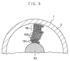
- Fig. 3 is an explanatory section of another embodiment of a composite body prior to undergoing extrusion which is incorporated in a Cu billet, and wherein numeral 4b denotes Cu base metal rod.
- Nb single core wires 13c and 13d Two types of Nb single core wires 13c and 13d were formed which would be Nb base metal filaments in a superconducting wire precursor. Specifically, an Nb base metal rod having a diameter of 11 mm in the form of round bar was inserted into a Cu base metal pipe having inner and outer diameters of 11.8 mm and 16.8 mm, and the resultant was drawn to have a wire diamter of 4.2 mm and to form the single core wire 13c with a small Cu thickness.
- This composite wire was inserted into a Ta pipe serving as a barrier material against Sn diffusion and further into a Cu pipe for stabilization to achieve a secondary composition.
- the resultant was drawn to have a wire diameter of 0.5 mm to yield a superconducting wire precursor.
- the superconducting wire precursor was subjected to a preheating then to a heat treatment at 600° to 750°C for 100 to 200 hours to yield an Nb-Sn superconducting wire.
- Fig. 4 is an explanatory section of the thus manufactured superconducting wire having been heat-treated, and wherein denoted at numeral 9 is the superconducting wire after undergoing heat treatment, at numeral 10 Nb3Sn filament, at numeral 11 low-Sn-concentration bronze layer, at numeral 7 barrier layer of Ta, and at numeral 8 stabilizing material of Cu.
- the superconducting wire thus obtained was measured for Jc and d eff in liquid helium.
- the superconducting wire thus obtained is compared with a conventional one by totally estimating these in terms of Jc/d eff , the superconducting wire of the present invention is found to have been improved 5.6 times the conventional one.
- the Cu base metal material 4c in the form of disk was formed in the following manner. 309 apertures of 4.95 mm diameter were formed in an oxygen-free copper disk of 160 mm diameter and 10 mm thickness using an NC drilling machine. In this case, apertures between the innermost first and second layers (counted radially) were arranged closely to each other, those between the second and fourth layers sparsely, and those between the fourth and outermost fifth layers closely. 30 pieces of the Cu base metal material disk 4c were stuffed in a billet container of oxygen-free copper of 180 mm outer diameter and 160 mm inner diameter with their apertures registered with each other. Nb base metal rods 13 of 4.9 mm diameter were inserted into the apertures of the stacked Cu disks, respectively. Finally, air in the billet was evacuated, and a cover was welded to the billet to form a composite billet. Insertion of the Nb base metal rods into the oxygen-free copper disks in stacks was conducted with ease.
- the composite billet was extruded and centrally formed with an aperture into which an Sn base metal rod was then inserted.
- the resultant was drawn to form a composite wire.
- the composite wire was inserted in a Ta pipe serving as a barrier material against Sn diffusion, and the resultant was further inserted into a Cu pipe to achieve secondary composition, followed by being drawn to have a wire diameter of 0.5 mm.
- the superconducting wire precursor thus formed was subjected to a preheating then to a heat treatment at 600° to 750°C for 100 to 200 hours to yield an Nb-Sn superconducting wire.
- a superconducting wire may be required to be improved in Jc characteristic more than in d eff characteristic.
- such an arrangement is offered in this Example that single core wires are disposed so that Nb base metal filaments would exist only in the region outside the boundary of the aforementioned ⁇ -phase bronze layer when ⁇ -phase bronze layer is produced during the heat treatment. This arrangement avoids Nb3Sn filaments from coming into mutual contact or coupling while effectively reducing the d eff value.
- the Nb single core wires and Cu base metal wire a were stuffed in a billet with an arragement wherein radially from the center were disposed seven layers of Cu base metal wire 4a, three layers of single core wire 13f, and seven layers of single core wire 13e.
- Fig. 7 depicts only a single line of single core wires 13e and 13f and Cu base metal wire 4a which is radially drawing though these wires are stuffed in the overall section.
- the resulting billet was sucbjected to extrusion, the extruded composite body was centrally formed with an aperture, and an Sn alloy rod of 14 mm diameter containing 1.5 % by weight of Ti was inserte into the aperture, followed by drawing the resultant to form a composite wire.
- the composite wire is circumferentially plated with Sn to about 30 ⁇ m thickness, inserted into a Ta pipe serving as a barrier material against Sn diffusion, and further inserted into a Cu pipe for stabilization to achieve secondary composition, followed by being drawn to have a wire diameter of 0.5 mm.
- Sn plating was conducted is that by diffusing Sn to the outer portion the amount of the Sn base metal material to be centrally located is reduced thereby minimizing the area of the ⁇ -phase bronze layer to be produced by the centrally-located Sn.
- the superconducting wire precursor was subjected to a preheating and then to a heat treatment at 600°C to 800°C for 100 to 200 hours to yield an Nb-Sn superconducting wire.
- the temperature for this heat treatment needs to be a temperature causing a thermal diffusion reaction, thus forming a superconductor.
- the heat treatment temperature is from 600° to 800°C.
- Fig. 9 is an explanatory section showing a superconducting wire precursor according to the second aspect of the present invention, which has been reduced in section area by drawing and has not yet been subjected to a heat treatment.
- the superconducting wire precursor 21 comprises a composite body 22 of Cu base metal material and Sn base metal material, and Nb base metal filaments 23.
- Fig. 10 is an explanatory section showing a superconducting wire obtained by subjecting the superconducting wire precursor to the heat treatment.
- the superconducting wire 24 in Fig. 10 comprises Nb3Sn filaments 25, and bronze layer 26 of which Sn concentration is lowered by a reaction of Nb with Sn diffused by the heat treatment.
- the composite body 22 of the Cu base metal material and Sn base metal material was formed in the following manner. First, thick plates of 15 mm thickness each resulting from rolling and integrating ten oxygen-free copper plates of 2 mm thickness and nine Sn plates of 1 mm thickess in an alternately stacked fashion were tightly stuffed in an oxygen-free copper container of 180 mm outer diameter and 160 mm inner diameter along the length thereof. Next, air in the container was evacuated, a cover was welded to the container, and the resultant was subjected to cold hydrostatic extrusion to form a composite in the form of a rod of 90 mm diameter. Finally, the oxygen-free copper in an outer peripheral portion of this composite rod was eliminated by external cutting using a lathe to form a columnar composite 22 of 80 mm diameter.
- the composite 22 was cut to a length of 100 mm and then drilled to form 127 apertures of 4.1 mm diameter.
- Nb base metal wires of 4.0 mm diameter and 100 mm length were individually inserted into the apertures of the composite, and the resultant was accommodated in an oxygen-free copper container of 90 mm outer diameter and 80 mm inner diameter. Air in the container was evacuated, and a cover was welded to the container by electron beam welding to form a composite billet.
- the composite billet was subjected to cold hydrostatic extrusion and then eliminated of oxygen-free copper in an outer peripheral portion thereof by external cutting using a lathe.
- the resultant was drawn to have a final diameter and then twisted to form a superconducting wire precursor of 0.2 wire diameter.
- the thus obtained superconducting wire precursor was subjected to a preheating then to a heat treatment at 600° to 800°C for 50 to 200 hours to form a superconducting wire having Nb3Sn superconductor produced in the Nb base filament portion.
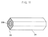
- Fig. 11 is an explanatory view showing one embodiment of a composite single core wire which will provide an Nb base metal filament in a superconducting wire precursor according to the second aspect of the present invention.
- the composite single core wire comprises Nb base metal rod 23b containing 1 % by weight of Ti, Cu base metal material 28, and Sn plated layer 29 covering the Cu base metal material.
- This composite single core wire was formed in the following manner. An Nb base metal rod of 11 mm diameter incorporated with 1 % by weight of Ti was inserted into a Cu pipe of 11.8 mm inner diameter and 18.4 mm outer diameter, and the resultant was drawn to form a hexagonal single core wire of 4.2 mm across flats. The single core wire was covered with an Sn-plated layer 29 of about 100 ⁇ m thickness to yield the composite single core wire shown in Fig. 11.
- An oxygen-free copper billet of 180 mm outer diameter and 160 mm inner diameter was stuffed with 1225 pieces of the composite single core wire thus formed, air in the billet was evacuated, and a cover was welded to the billet by electron beam welding to form a composite billet.
- the composite billet was subjected to cold hydrostatic extrusion and drawn to form a composite body.
- the resultant composite body was inserted into a Ta pipe serving as a barrier material against Sn diffusion, and further inserted into a Cu pipe for stabilization to achieve secondary composition, followed by being drawn to have a final wire diameter.
- the composite body having the final diameter was twisted to yield a superconducting wire precursor of 0.3 mm wire diameter.
- an Nb base metal rod of 13.9 mm diameter was centrally inserted into an oxygen-free copper billet container of 25 mm outer diameter and 14 mm inner diameter having eight apertures of 3.5 mm diameter as shown in Fig. 14.
- Eight Sn base metal rods of 3.4 mm diameter containing 7 % by weight of In were individually inserted into the apertures lying around the center of the container.
- Air in the billet container was evacuated, a cover was welded to the billet container by electron beam welding.
- the resultant container was subjected to cold hydrostatic extrusion and then drawn to form a hexagonal composite single core wire of 4.2 mm across flats.
- a Cu billet similar to that in Example 6 was stuffed with 1225 pieces of the single core wire thus formed, air in the billet was evacuated, and a cover was welded by electron beam welding to form a composite billet.
- This composite billet was subjected to cold hydrostatic extrusion and then drawn to form a composite wire.
- the resultant composite wire was inserted into a Ta pipe to serve as a barrier material against Sn diffusion, and further inserted into a Cu pipe for stabilization to achieve secondary composition, followed by being drawn to have a final wire diameter.
- the composite wire of the final diameter was twisted to yield a superconducting wire precursor of 0.3 mm wire diameter.
- Fig. 15 is an explanatory section of the superconducting wire precursor thus obtained, and wherein superconducting wire precursor 21 comprises Nb base metal filaments 23a, Ta barrier layer 30, Cu layer 31 for stabilization, Cu base metal material 32, and Sn base metal material 34 containing 7 % by weight of In.
- the thus obtained superconducting wire precursor was subjected to a preheating and then to a heat treatment at 600° to 800°C for 50 to 200 hours to form a superconducting wire having Nb3Sn superconductor produced in the Nb base metal filament portion.
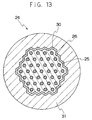
- the sectional structure of the thus obtained superconducting wire was similar to that shown in Fig. 13.
- Fig. 16 is an explanatory view showing a constitution of a composite single core wire prior to being reduced in section area for use in manufacturing a superconducting wire according to the second aspect of the present invention.
- the composite single core wire comprises composite body 22b of Cu containing 1 % by weight of Ti and Sn, and Nb base metal rod 23a.
- Fig. 17 is an explanatory section of the superconducting wire precursor thus obtained, and wherein superconducting wire precursor comprises a composite body 22b of Cu containing 1 % by weight of Ti and Sn, Nb base metal filaments 23a, Ta barrier layer 30, Cu layer 31 for stabilization, and Cu base metal material 32.
- the thus obtained superconducting wire precursor was subjected to a preheating and then to a heat treatment at 600° to 800°C for 50 to 200 hours to form a superconducting wire having Nb3Sn superconductor produced in the Nb base metal filament portion.
- the sectional structure of the thus obtained superconducting wire was similar to that shown in Fig. 13.
- the superconducting wire thus obtained was measured for Jc and d eff in liquid helium.
- the measurement revealed that the Jc value of this supercoducting wire was 900 A/mm2 in a magnetic field of B 12 T and the d eff value was 3 ⁇ m.
- this superconducting wire thus obtained is compared with an Nb3Sn superconducting wire containing Ti and obtained by the prior art internal diffusion method by totally estimating the two in terms of Jc/d eff , this superconducting wire of the present invention is found to have been improved 7.5 times the prior art superconducting wire.
- Fig. 18 is an explanatory view showing a constitution of a composite single core wire prior to being reduced in section area for use in manufacturing a superconducting wire according to the second aspect of the present invention.
- the composite single core wire comprises composite body 22c of a Cu base metal material plated on its surface with Sn, Nb base metal rod 23c plated on its surface with Ti, and oxygen-free copper pipe 35.
- An Nb base metal rod of 10 mm diameter which become a filament of a superconducting wire was electro-coated with a Ti layer of about 45 ⁇ m thickness.
- An oxygen-free copper plate of about 200 mm width and 0.5 mm thickness was plated with an Sn layer of about 0.1 mm to form a Cu-Sn composite body 22c.
- the composite body 22c was wound about five times around the Ti-plated Nb base metal rod 23c as a core, then inserted into oxygen-free copper pipe 35 of 18 mm inner diameter and 19 mm outer diameter, followed by being drawn to form a hexagonal composite single core wire of 4.2 mm across section.
- a Cu billet similar to that used in Example 6 was stuffed with 1225 pieces of the composite single core wire thus formed, air in the billet was evacuated, and a cover was welded to the billet by electron beam welding. The resultant was then subjected to cold hydrostatic extrusion and drawn to form a composite wire. The composite wire thus formed was further drawn to have a final wire diameter and then twisted to form a superconducting wire precursor of 0.3 mm wire diameter.
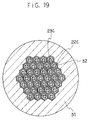
- Fig. 19 is an explanatory section of the superconducting wire precursor thus obtained, wherein the superconducting wire precursor comprises Cu composite body 22c plated on its surface with Sn, Nb base metal filaments 23c plated on its surface with Ti, Cu layer 31 for stabilization, and Cu base metal material 32.
- the superconducting wire thus obtained was measured for Jc and d eff in liquid helium.
- the measurement revealed that the Jc value of this supercoducting wire was 900 A/mm2 in a magnetic field of B 12T and the d eff value was 3 ⁇ m.
- this superconducting wire thus obtained is compared with an Nb3Sn superconducting wire containing Ti and obtained by the prior art internal diffusion method by totally estimating the two in terms of Jc/d eff , this superconducting wire of the present invention is found to have been improved 7.5 times the prior art superconducting wire.
- Fig. 20 is an explanatory section view showing a constitution of a composite single core wire prior to being reduced in section area for use in manufacturing a superconducting wire according to the second aspect of the present invention.
- the composite single core wire comprises Cu-Sn composite body 22c composed of a Cu base metal material plated on its both sides with Sn, Nb base metal rod 23a, Cu base metal pipe 35, and Ti thin plate 36 sandwiched between the Cu-Sn composite body 22c and the Nb base metal rod 23a.
- Single core wire 1 which becomes a filament of a superconducting wire was formed in the following manner.
- an oxygen-free copper plate of about 200 mm width and 0.5 mm thickness was plated with Sn in about 0.1 mm thickness to form the Cu-Sn composite body 22c.
- Ti thin plate 36 of 0.05 mm thickness and about 30 mm width was stacked on the composite body 22c.
- the composite body 22c with the Ti thin plate 36 was wound about five times around the Nb base metal rod 23a of 10 mm diameter as a core. Since the Ti thin plate 36 was of only about 30 mm width, it was wound around the Nb base metal rod only in a layer.
- the resultant was then inserted into oxygen-free copper pipe 35 of 18 mm inner diameter and 19 mm outer diameter, followed by being drawn to form a hexagonal composite single core wire of 4.2 mm across section.
- a Cu billet similar to that used in Example 6 was stuffed with 1225 pieces of the composite single core wire thus formed, air in the billet was evacuated, and a cover was welded to the billet by electron beam welding. The resultant was then subjected to cold hydrostatic extrusion and drawn to form a composite wire.
- the composite wire was inserted into a Ta pipe serving as a barrier material against Sn diffusion and further inserted into a Cu pipe for stabilization to achieve secondary composition.
- the secondary composition thus formed was further drawn to have a final wire diameter and then twisted to form a superconducting wire precursor of 0.3 mm wire diameter.
- the thus obtained superconducting wire precursor was subjected to a preheating and then to a heat treatment at 600° to 800°C for 50 to 200 hours to form a superconducting wire having Nb3Sn superconductor produced in the Nb base metal filament portion.
- the sectional structure of the thus obtained superconducting wire was similar to that shown in Fig. 13.
- the superconducting wire thus obtained was measured for Jc and d eff in liquid helium.
- the measurement revealed that the Jc value of this supercoducting wire was 900 A/mm2 in a magnetic field of B 12T and the d eff value was 3 ⁇ m.
- this superconducting wire thus obtained is compared with an Nb3Sn superconducting wire containing Ti and obtained by the prior art internal diffusion method by totally estimating the two in terms of Jc/d eff , this superconducting wire of the present invention is found to have been improved 7.5 times the prior art superconducting wire.
- a thin plate of 1 mm thickness was formed by rolling to integrate a stack of two Cu plates of 1 mm thickness and an Sn plate of 1 mm thickness sandwiched between the Cu plates.
- the thin plate was cut to a size of 140 mm X 1000 mm and then plated on its one side with a Ti layer of about 10 ⁇ m thickness to form the composite body 22d.
- the composite body 22d was then wound several times around an Nb base metal rod 23a of 10 mm diameter and 1000 mm length in the form of round bar.
- the resultant was inserted into an oxygen-free copper pipe 35 of 18 mm inner diameter and 19 mm outer diameter, and drawn to form a hexagonal composite single core wire of 4.2 mm across flats.
- a Cu billet similar to that used in Example 6 was stuffed with 1225 pieces of the composite single core wire thus formed, air in the billet was evacuated, and a cover was welded to the billet by electron beam welding.
- This billet was subjected to cold hydrostatic extrusion and then drawn to form a composite wire.
- the resultant composite wire was inserted into a Ta pipe serving as a barrier material against Sn diffusion, and further inserted into a Cu pipe for stabilization to achieve secondary composition, followed by being drawn to have a final wire diameter.
- the composite wire of the final diameter was twisted to yield a superconducting wire precursor of 0.3 mm diameter.
- the sectional structure of the thus obtained superconducting wire precursor was as shown in Fig. 17.
- the thus obtained superconducting wire precursor was subjected to a preheating and then to a heat treatment at 600° to 800°C for 50 to 200 hours to form a superconducting wire having Nb3Sn superconductor produced in the Nb base metal filament portion.
- the sectional structure of the thus obtained superconducting wire was similar to that shown in Fig. 13.
- the superconducting wire thus obtained was measured for Jc and d eff in liquid helium.
- the measurement revealed that the Jc value of this supercoducting wire was 910 A/mm2 in a magnetic field of B 12T and the d eff value was 3 ⁇ m.
- this superconducting wire thus obtained is compared with an Nb3Sn superconducting wire containing Ti and obtained by the prior art internal diffusion method by totally estimating the two in terms of Jc/d eff , this superconducting wire of the present invention is found to have been improved 7.5 times the prior art superconducting wire.
- a superconducting wire may be required to be improved in Jc characteristic rather than in d eff characteristic.
- such an arrangement is offered in this Example that filaments are disposed more tightly than in the foregoing Examples. This arrangement makes it possible to improve Jc characteristic though mutual coupling of the Nb3Sn filaments occurs to some extent after the heat treatment thereby to increase d eff characteristic.
- a thin plate of 1.5 mm thickness was formed by rolling to integrate a stack of two Cu plates of 1 mm thickness and an Sn plate of 1.5 mm thickness sandwiched between the Cu plates.
- the thin plate was cut to a size of 150 mm X 1000 mm and then wound several times around an Nb base metal round rod 23d of 12.7 mm diameter and 1000 mm length which contained 1 % by weight of Ta.
- the resultant was inserted into the Cu pipe 36 of 19 mm inner diameter and 20 mm outer diameter containing 3 % by weight of Ti, followed by being drawn to form a hexagonal composite single core wire of 4.2 mm across flats.
- a Cu billet similar to that used in Example 6 was stuffed with 1225 pieces of the single core wire thus formed, air in the billet was evacuated, and a cover was welded to the billet by electron beam welding.
- This billet was subjected to cold hydrostatic extrusion and then drawn to form a composite wire.
- the resultant composite wire was inserted into a Ta pipe serving as a barrier material against Sn diffusion, and further inserted into a Cu pipe for stabilization to achieve secondary composition, followed by being drawn to have a final diameter.
- the composite wire of the final diameter was twisted to yield a superconducting wire precursor of 0.3 mm wire diameter.
- the sectional structure of the thus obtained superconducting wire precursor was as shown in Fig. 11.
- the superconducting wire precursor was subjected to a preheating and then to a heat treatment at 600° to 800°C for 50 to 200 hours to form a superconducting wire having Nb3Sn superconductor in the Nb base metal filament portion.
- the sectional structure of the thus obtained superconducting wire was similar to that shown in Fig. 13.
- the superconducting wires obtained by the dispersed Sn diffusion method in Examples 5 to 12 are totally estimated in terms of Jc/d eff value, they are found to have been improved in superconducting characteristics about five to about seven times the superconducting wire obtained by the prior art internal diffusion method.
- the superconducting wires prepared in Examples 8 to 12 by a method wherein the Cu-Sn composite body was wound several times around the Nb round bar have remarkably improved superconducting characteristics such as Jc value, d eff value and n value, and further have an excellent processability. This is conceivably because winding the composite body several times around the Nb bar improved the dispersion of Sn and avoided the formation of non-uniform distribution of Nb3Sn produced in filament, leading to improved superconducting characteristics.
- the superconducting wires prepared in the foregoing Examples 5 to 12 are those having a stabilizing layer of Cu and a diffusion barrier layer of Ta, it should be understood that use of Al of high purity for the stabilizing layer and Nb or V for the diffusion barrier layer are also effective, and that the provision of the stabilizing layer and diffusion barrier layer may be omitted.
- the spacing between adjacent Nb base metal filaments is enlarged to such an extent that mutual contact of Nb3Sn filaments to be produced during the heat treatment will not occur in the region where the boundary of ⁇ -phase bronze layer appears during the preheating treatment for diffusing the Sn base metal material.
- mutual coupling of Nb3Sn filaments in the superconducting wire due to mutual contact thereof can be avoided, and further the effective filament diameter of the superconducting wire can be reduced with a decrease in Jc value suppressed to minimum. This results in a substantial reduction in hysteresis loss produced upon conduction of pulse current and leads to a superconducting coil of improved stability.
- a composite material composed of a base metal material X such as Sn or Ga and Cu is dispersedly disposed around individual filaments of a base metal material Z such as Nb or V, whereby the spacing between adjacent filaments can be increased by about 30 % as compared with that according to the prior art internal diffusion method.
- a compound superconducting wire comprising a matrix of CuX alloy and a multiplicity of Z3X filaments embedded in the matrix in a spaced relationship so as not to come into contact with each other wherein X is Sn or Ga and Z3X is Nb3Sn or V3Ga, which is prepared according to an internal diffusion process from (1) a precursor wire comprising a Cu base metal matrix, a core of a base metal material X such as Sn arranged in the center portion of the wire and a multiplicity of filaments of a base metal material Z such as Nb arranged concentrically in layers around the core, in which the spacing between any adjacent filaments arranged in a boundary region of an ⁇ -phase bronze layer having a certain radius from the center produced when the precursor is preheat-treated at a temperature of 300° to 600°C is made larger than the spacing between any adjacent filaments arranged in the other matrix regions so that the filaments do not come into contact with each other when heat-treated to convert the precursor into a superconducting wire; or
- the effective filament diameter is remarkably decreased, thus hysteresis loss is decreased to improve the stability of superconducting coils, and also the critical current density Jc and uniformity of the wire are improved.
Landscapes
- Engineering & Computer Science (AREA)
- Manufacturing & Machinery (AREA)
- Superconductors And Manufacturing Methods Therefor (AREA)
Applications Claiming Priority (6)
| Application Number | Priority Date | Filing Date | Title |
|---|---|---|---|
| JP76841/93 | 1993-04-02 | ||
| JP7684193 | 1993-04-02 | ||
| JP76837/93 | 1993-04-02 | ||
| JP7683793 | 1993-04-02 | ||
| JP5194781A JP3012436B2 (ja) | 1993-04-02 | 1993-08-05 | 化合物系超電導線およびその製法 |
| JP194781/93 | 1993-08-05 |
Publications (2)
| Publication Number | Publication Date |
|---|---|
| EP0618627A1 true EP0618627A1 (de) | 1994-10-05 |
| EP0618627B1 EP0618627B1 (de) | 1998-03-11 |
Family
ID=27302269
Family Applications (1)
| Application Number | Title | Priority Date | Filing Date |
|---|---|---|---|
| EP93120670A Expired - Lifetime EP0618627B1 (de) | 1993-04-02 | 1993-12-22 | Zusammengesetzter supraleitender Draht und Verfahren zu seiner Herstellung |
Country Status (4)
| Country | Link |
|---|---|
| US (2) | US5753862A (de) |
| EP (1) | EP0618627B1 (de) |
| JP (1) | JP3012436B2 (de) |
| DE (1) | DE69317408T2 (de) |
Cited By (1)
| Publication number | Priority date | Publication date | Assignee | Title |
|---|---|---|---|---|
| EP2466660A3 (de) * | 2010-12-14 | 2013-10-23 | SH Copper Products Co., Ltd. | Vorläufer für einen supraleitenden Nb3Sn-Draht, Verfahren zu dessen Herstellung, supraleitender Nb3Sn-Draht und supraleitendes Magnetsystem |
Families Citing this family (14)
| Publication number | Priority date | Publication date | Assignee | Title |
|---|---|---|---|---|
| FR2770928B1 (fr) * | 1997-11-13 | 1999-12-31 | Gec Alsthom Electromec | Procede de fabrication d'un brin supraconducteur multifilamentaire, stable et a pertes reduites |
| US6568060B1 (en) * | 1999-06-04 | 2003-05-27 | Polymet Corporation | Method and fixture for filled billet packing |
| JP2001236836A (ja) * | 2000-02-21 | 2001-08-31 | Hitachi Cable Ltd | Nb3Sn系超電導線材 |
| JP3946966B2 (ja) * | 2001-04-19 | 2007-07-18 | 三菱電機株式会社 | Sn−Ti系化合物を含むSn基合金の製造方法 |
| US6642158B1 (en) * | 2002-09-23 | 2003-11-04 | Intel Corporation | Photo-thermal induced diffusion |
| US6981309B2 (en) * | 2003-10-17 | 2006-01-03 | Oxford Superconducting Technology | Method for producing (Nb, Ti)3Sn wire by use of Ti source rods |
| US7216418B2 (en) * | 2003-10-23 | 2007-05-15 | Oxford Superconducting Technology | Method for using divider rods for separating superconducting regions in fine filament internal tin wire |
| WO2006038909A2 (en) * | 2004-02-19 | 2006-04-13 | Oxford Superconducting Technology | IMPROVING CRITICAL DENSITY IN Nb3Sn SUPERCONDUCTING WIRE |
| JP2006004684A (ja) * | 2004-06-16 | 2006-01-05 | Mitsubishi Electric Corp | 超電導線材の製造方法 |
| JP2006032190A (ja) * | 2004-07-20 | 2006-02-02 | Mitsubishi Electric Corp | Nb−Sn化合物系超電導線及びその前駆体 |
| JP2006066274A (ja) * | 2004-08-27 | 2006-03-09 | Mitsubishi Electric Corp | Nb−Sn化合物系超電導線の前駆線材 |
| US20060272145A1 (en) * | 2005-03-11 | 2006-12-07 | Alabama Cryogenic Engineering, Inc. | Method of producing superconducting wire and articles produced thereby |
| JP5794560B2 (ja) * | 2011-01-18 | 2015-10-14 | 国立研究開発法人物質・材料研究機構 | 混合バリア型Nb3Al超電導線材 |
| CN102254621B (zh) * | 2011-04-07 | 2012-11-21 | 西部超导材料科技有限公司 | 一种内锡法Nb3Sn超导线的热处理方法 |
Citations (4)
| Publication number | Priority date | Publication date | Assignee | Title |
|---|---|---|---|---|
| JPS63216212A (ja) * | 1987-03-03 | 1988-09-08 | Agency Of Ind Science & Technol | Nb↓3Sn系化合物超電導線並びにその製造方法 |
| US4973365A (en) * | 1989-06-06 | 1990-11-27 | Advanced Superconductors, Inc. | Process for producing monocore precursor Nb3 Sn superconductor wire |
| WO1991004583A1 (en) * | 1989-09-25 | 1991-04-04 | Teledyne Wah Chang Albany | Alloy core modification for tin core superconducting materials |
| JPH04289615A (ja) * | 1991-03-12 | 1992-10-14 | Mitsubishi Electric Corp | 化合物超電導線材の製造方法 |
Family Cites Families (35)
| Publication number | Priority date | Publication date | Assignee | Title |
|---|---|---|---|---|
| GB1333554A (en) * | 1969-10-27 | 1973-10-10 | Atomic Energy Authority Uk | Superconducting members and methods of manufacture thereof |
| US3710000A (en) * | 1970-05-13 | 1973-01-09 | Air Reduction | Hybrid superconducting material |
| US3905839A (en) * | 1971-12-17 | 1975-09-16 | Gen Electric | Liquid sintered cobalt-rare earth intermetallic product |
| US3838503A (en) * | 1972-07-12 | 1974-10-01 | Atomic Energy Commission | Method of fabricating a composite multifilament intermetallic type superconducting wire |
| US3763553A (en) * | 1972-09-26 | 1973-10-09 | Imp Metal Ind Kynoch Ltd | Method of fabricating intermetallic type superconductors |
| DE2331962A1 (de) * | 1973-06-22 | 1975-01-16 | Siemens Ag | Verfahren zum herstellen eines supraleiters mit einer supraleitenden intermetallischen verbindung aus zwei elementen |
| DE2331919C3 (de) * | 1973-06-22 | 1978-12-07 | Siemens Ag, 1000 Berlin U. 8000 Muenchen | Verfahren zum Herstellen eines Supraleiters mit einer supraleitenden intermetallischen Verbindung aus wenigstens zwei Elementen |
| DE2333893C3 (de) * | 1973-07-03 | 1975-12-11 | Siemens Ag, 1000 Berlin Und 8000 Muenchen | Verfahren zum Herstellen eines Supraleiters mit einer aus wenigstens zwei Elementen bestehenden supraleitenden intermetallischen Verbindung |
| US3930903A (en) * | 1974-02-07 | 1976-01-06 | Supercon, Inc. | Stabilized superconductive wires |
| US3910802A (en) * | 1974-02-07 | 1975-10-07 | Supercon Inc | Stabilized superconductors |
| US3958327A (en) * | 1974-05-01 | 1976-05-25 | Airco, Inc. | Stabilized high-field superconductor |
| CH584449A5 (de) * | 1975-03-12 | 1977-01-31 | Bbc Brown Boveri & Cie | |
| CH586952A5 (de) * | 1975-03-26 | 1977-04-15 | Bbc Brown Boveri & Cie | |
| JPS5216997A (en) * | 1975-07-31 | 1977-02-08 | Toshiba Corp | Processing method of multi-superconductor |
| US4073666A (en) * | 1976-09-09 | 1978-02-14 | Airco, Inc. | Method for making an insulated superconductor and article produced thereby |
| EP0054421B1 (de) * | 1980-12-15 | 1985-05-15 | The BOC Group, Inc. | Verfahren zum Herstellen vieladriger Supraleiter aus einer intermetallischen Verbindung |
| DE3207159A1 (de) * | 1982-02-27 | 1983-09-08 | Vacuumschmelze Gmbh, 6450 Hanau | Verfahren zur herstellung eines stabilisierten supraleiters mit einer diffusionshemmenden schicht |
| FR2543741B1 (fr) * | 1983-03-16 | 1985-06-14 | Comp Generale Electricite | Procede de fabrication de supraconducteurs |
| US4743713A (en) * | 1984-02-10 | 1988-05-10 | United States Department Of Energy | Aluminum-stabilized NB3SN superconductor |
| JPS6116141A (ja) * | 1984-06-29 | 1986-01-24 | Nissan Motor Co Ltd | 自動車のフツトレスト取付構造 |
| JPH0768605B2 (ja) * | 1985-01-18 | 1995-07-26 | 株式会社フジクラ | Nb▲下3▼Sn系超電導線材の製造方法 |
| DE3531769A1 (de) * | 1985-09-06 | 1987-03-19 | Kernforschungsz Karlsruhe | Verfahren zur herstellung von multifilament-supraleiterdraehten aus nb(pfeil abwaerts)3(pfeil abwaerts)sn- oder v(pfeil abwaerts)3(pfeil abwaerts)ga-filamenten, eingebettet in einer cu- oder cu-legierungs-matrix, welche metallische zusatzelemente enthalten, mit vorbestimmten supraleitenden eigenschaften |
| DE3540070A1 (de) * | 1985-11-12 | 1987-05-14 | Siemens Ag | Supraleitender verbundleiter mit mehreren leiteradern und verfahren zu dessen herstellung |
| JPS62174354A (ja) * | 1986-01-25 | 1987-07-31 | Natl Res Inst For Metals | Ti添加Nb3Sn複合超電導線材の製造法 |
| US4860431A (en) * | 1988-02-17 | 1989-08-29 | Oxford Superconducting Technology | Fabrication of multifilament intermetallic superconductor using strengthened tin |
| EP0346124B2 (de) * | 1988-06-09 | 1998-05-06 | Kabushiki Kaisha Toshiba | Zusammengesetzter supraleitender Draht und Verfahren zu dessen Herstellung |
| US5174831A (en) * | 1989-06-08 | 1992-12-29 | Composite Materials Technology, Inc. | Superconductor and process of manufacture |
| US5174830A (en) * | 1989-06-08 | 1992-12-29 | Composite Materials Technology, Inc. | Superconductor and process for manufacture |
| FR2649530B1 (fr) * | 1989-07-06 | 1994-04-29 | Alsthom Gec | Brin supraconducteur multifilamentaire |
| US5088183A (en) * | 1990-05-01 | 1992-02-18 | Kanithi Hem C | Process for producing fine and ultrafine filament superconductor wire |
| US5139893A (en) * | 1990-05-17 | 1992-08-18 | Composite Materials Technology, Inc. | Superconducting alloy core circumscribed by multiple layers of NbTi and refractory metal barrier layer having a normal metal sheath |
| GB9014966D0 (en) * | 1990-07-06 | 1990-08-29 | Walters Colin R | Component and method for fabricating superconducting wire |
| GB9014979D0 (en) * | 1990-07-06 | 1990-08-29 | Walters Colin R | Method of fabricating an elongated artefact |
| US5228928A (en) * | 1991-02-07 | 1993-07-20 | The Furukawa Electric Co., Ltd. | Method of manufacturing Nb3 Sn superconducting wire |
| US5501746A (en) * | 1993-12-16 | 1996-03-26 | Mitsubishi Denki Kabushiki Kaisha | Process for preparing superconducting wire |
-
1993
- 1993-08-05 JP JP5194781A patent/JP3012436B2/ja not_active Expired - Lifetime
- 1993-12-16 US US08/167,061 patent/US5753862A/en not_active Expired - Fee Related
- 1993-12-22 EP EP93120670A patent/EP0618627B1/de not_active Expired - Lifetime
- 1993-12-22 DE DE69317408T patent/DE69317408T2/de not_active Expired - Lifetime
-
1997
- 1997-04-04 US US08/832,796 patent/US5926942A/en not_active Expired - Fee Related
Patent Citations (4)
| Publication number | Priority date | Publication date | Assignee | Title |
|---|---|---|---|---|
| JPS63216212A (ja) * | 1987-03-03 | 1988-09-08 | Agency Of Ind Science & Technol | Nb↓3Sn系化合物超電導線並びにその製造方法 |
| US4973365A (en) * | 1989-06-06 | 1990-11-27 | Advanced Superconductors, Inc. | Process for producing monocore precursor Nb3 Sn superconductor wire |
| WO1991004583A1 (en) * | 1989-09-25 | 1991-04-04 | Teledyne Wah Chang Albany | Alloy core modification for tin core superconducting materials |
| JPH04289615A (ja) * | 1991-03-12 | 1992-10-14 | Mitsubishi Electric Corp | 化合物超電導線材の製造方法 |
Non-Patent Citations (2)
| Title |
|---|
| PATENT ABSTRACTS OF JAPAN vol. 013, no. 005 (E - 701) 9 January 1989 (1989-01-09) * |
| PATENT ABSTRACTS OF JAPAN vol. 017, no. 097 (E - 1326) 25 February 1993 (1993-02-25) * |
Cited By (4)
| Publication number | Priority date | Publication date | Assignee | Title |
|---|---|---|---|---|
| EP2466660A3 (de) * | 2010-12-14 | 2013-10-23 | SH Copper Products Co., Ltd. | Vorläufer für einen supraleitenden Nb3Sn-Draht, Verfahren zu dessen Herstellung, supraleitender Nb3Sn-Draht und supraleitendes Magnetsystem |
| US8778841B2 (en) | 2010-12-14 | 2014-07-15 | Sh Copper Products Co., Ltd. | Precursor for a Nb3Sn superconductor wire, method for manufacturing the same, Nb3Sn superconductor wire, and superconducting magnet system |
| US20140221215A1 (en) * | 2010-12-14 | 2014-08-07 | Sh Copper Products Co., Ltd. | Precursor for a nb3sn superconductor wire, method for manufacturing the same, nb3sn superconductor wire, and superconducting magnet system |
| US9177700B2 (en) | 2010-12-14 | 2015-11-03 | Sh Copper Products Co., Ltd. | Precursor for a Nb3Sn superconductor wire, method for manufacturing the same, Nb3Sn superconductor wire, and superconducting magnet system |
Also Published As
| Publication number | Publication date |
|---|---|
| EP0618627B1 (de) | 1998-03-11 |
| DE69317408D1 (de) | 1998-04-16 |
| JP3012436B2 (ja) | 2000-02-21 |
| US5753862A (en) | 1998-05-19 |
| DE69317408T2 (de) | 1998-07-30 |
| JPH06338228A (ja) | 1994-12-06 |
| US5926942A (en) | 1999-07-27 |
Similar Documents
| Publication | Publication Date | Title |
|---|---|---|
| US5926942A (en) | Method for manufacturing superconducting wire | |
| US4990411A (en) | Compound superconducting wire and method of manufacturing the same | |
| US4973365A (en) | Process for producing monocore precursor Nb3 Sn superconductor wire | |
| US4161062A (en) | Method for producing hollow superconducting cables | |
| US6251529B1 (en) | Nb-Sn compound superconducting wire precursor, method for producing the same and method for producing Nb-Sn compound superconducting wire | |
| US4055887A (en) | Method for producing a stabilized electrical superconductor | |
| EP2099080A1 (de) | Supraleitender Nb3Sn-Draht, der mit einem internen Sn-Verfahren hergestellt wird, und Vorläuferverbindung zum Herstellen des Drahts | |
| US4646428A (en) | Method of fabricating multifilament intermetallic superconductor | |
| EP1993153A1 (de) | Nb3Sn-Supraleiter, Vorläufer dafür und Verfahren zu Herstellung eines Vorläufers | |
| US4224735A (en) | Method of production multifilamentary intermetallic superconductors | |
| US5554448A (en) | Wire for Nb3 X superconducting wire | |
| US5127149A (en) | Method of production for multifilament niobium-tin superconductors | |
| US11990251B2 (en) | Methods for manufacturing a superconductor | |
| US4447946A (en) | Method of fabricating multifilament intermetallic superconductor | |
| US4084989A (en) | Method for producing a stabilized electrical superconductor | |
| US4153986A (en) | Method for producing composite superconductors | |
| EP0609804B1 (de) | Verfahren zur Herstellung eines Nb3X supraleitenden Drahtes | |
| JP3273764B2 (ja) | 化合物系超電導線の製造方法 | |
| EP0718898B1 (de) | Draht aus supraleitender Verbindung | |
| JP3505894B2 (ja) | 化合物系超電導線材 | |
| JPH087681A (ja) | A3 b型化合物超電導線およびその製造方法 | |
| JPH09147635A (ja) | A15型超電導線材およびその製造方法 | |
| Yamada et al. | Wire for Nb 3 X superconducting wire | |
| JPH05334930A (ja) | 化合物超電導線用の複合ビレット、及び化合物超電導線の製造方法 | |
| JPH08212847A (ja) | 複合多芯超電導線 |
Legal Events
| Date | Code | Title | Description |
|---|---|---|---|
| PUAI | Public reference made under article 153(3) epc to a published international application that has entered the european phase |
Free format text: ORIGINAL CODE: 0009012 |
|
| AK | Designated contracting states |
Kind code of ref document: A1 Designated state(s): DE FR GB |
|
| 17P | Request for examination filed |
Effective date: 19941207 |
|
| 17Q | First examination report despatched |
Effective date: 19950926 |
|
| GRAG | Despatch of communication of intention to grant |
Free format text: ORIGINAL CODE: EPIDOS AGRA |
|
| GRAG | Despatch of communication of intention to grant |
Free format text: ORIGINAL CODE: EPIDOS AGRA |
|
| GRAG | Despatch of communication of intention to grant |
Free format text: ORIGINAL CODE: EPIDOS AGRA |
|
| GRAH | Despatch of communication of intention to grant a patent |
Free format text: ORIGINAL CODE: EPIDOS IGRA |
|
| GRAH | Despatch of communication of intention to grant a patent |
Free format text: ORIGINAL CODE: EPIDOS IGRA |
|
| GRAA | (expected) grant |
Free format text: ORIGINAL CODE: 0009210 |
|
| AK | Designated contracting states |
Kind code of ref document: B1 Designated state(s): DE FR GB |
|
| REF | Corresponds to: |
Ref document number: 69317408 Country of ref document: DE Date of ref document: 19980416 |
|
| ET | Fr: translation filed | ||
| PLBE | No opposition filed within time limit |
Free format text: ORIGINAL CODE: 0009261 |
|
| STAA | Information on the status of an ep patent application or granted ep patent |
Free format text: STATUS: NO OPPOSITION FILED WITHIN TIME LIMIT |
|
| REG | Reference to a national code |
Ref country code: GB Ref legal event code: 727 |
|
| 26N | No opposition filed | ||
| REG | Reference to a national code |
Ref country code: GB Ref legal event code: 727A |
|
| REG | Reference to a national code |
Ref country code: GB Ref legal event code: 727B |
|
| REG | Reference to a national code |
Ref country code: GB Ref legal event code: SP |
|
| REG | Reference to a national code |
Ref country code: GB Ref legal event code: IF02 |
|
| PGFP | Annual fee paid to national office [announced via postgrant information from national office to epo] |
Ref country code: GB Payment date: 20101222 Year of fee payment: 18 |
|
| REG | Reference to a national code |
Ref country code: GB Ref legal event code: 746 Effective date: 20110513 |
|
| REG | Reference to a national code |
Ref country code: DE Ref legal event code: R084 Ref document number: 69317408 Country of ref document: DE Effective date: 20110506 Ref country code: DE Ref legal event code: R084 Ref document number: 69317408 Country of ref document: DE Effective date: 20110629 |
|
| PGFP | Annual fee paid to national office [announced via postgrant information from national office to epo] |
Ref country code: FR Payment date: 20130107 Year of fee payment: 20 |
|
| PGFP | Annual fee paid to national office [announced via postgrant information from national office to epo] |
Ref country code: DE Payment date: 20121219 Year of fee payment: 20 |
|
| GBPC | Gb: european patent ceased through non-payment of renewal fee |
Effective date: 20121222 |
|
| PG25 | Lapsed in a contracting state [announced via postgrant information from national office to epo] |
Ref country code: GB Free format text: LAPSE BECAUSE OF NON-PAYMENT OF DUE FEES Effective date: 20121222 |
|
| REG | Reference to a national code |
Ref country code: DE Ref legal event code: R071 Ref document number: 69317408 Country of ref document: DE |
|
| PG25 | Lapsed in a contracting state [announced via postgrant information from national office to epo] |
Ref country code: DE Free format text: LAPSE BECAUSE OF EXPIRATION OF PROTECTION Effective date: 20131224 |