EP0609536A2 - Méthode de fabrication de transistors MOS verticaux - Google Patents
Méthode de fabrication de transistors MOS verticaux Download PDFInfo
- Publication number
- EP0609536A2 EP0609536A2 EP93120324A EP93120324A EP0609536A2 EP 0609536 A2 EP0609536 A2 EP 0609536A2 EP 93120324 A EP93120324 A EP 93120324A EP 93120324 A EP93120324 A EP 93120324A EP 0609536 A2 EP0609536 A2 EP 0609536A2
- Authority
- EP
- European Patent Office
- Prior art keywords
- trenches
- mask
- doped
- substrate
- polysilicon
- Prior art date
- Legal status (The legal status is an assumption and is not a legal conclusion. Google has not performed a legal analysis and makes no representation as to the accuracy of the status listed.)
- Withdrawn
Links
- 238000000034 method Methods 0.000 title claims description 19
- 238000004519 manufacturing process Methods 0.000 title claims description 10
- 229910021420 polycrystalline silicon Inorganic materials 0.000 claims abstract description 33
- 229920005591 polysilicon Polymers 0.000 claims abstract description 33
- 239000000758 substrate Substances 0.000 claims abstract description 24
- 238000009413 insulation Methods 0.000 claims abstract description 16
- 229910052581 Si3N4 Inorganic materials 0.000 claims abstract description 13
- 238000005530 etching Methods 0.000 claims abstract description 13
- 230000003647 oxidation Effects 0.000 claims abstract description 12
- 238000007254 oxidation reaction Methods 0.000 claims abstract description 12
- 238000001465 metallisation Methods 0.000 claims abstract description 11
- VYPSYNLAJGMNEJ-UHFFFAOYSA-N Silicium dioxide Chemical compound O=[Si]=O VYPSYNLAJGMNEJ-UHFFFAOYSA-N 0.000 claims description 14
- 239000002019 doping agent Substances 0.000 claims description 10
- 238000002513 implantation Methods 0.000 claims description 10
- 229910052681 coesite Inorganic materials 0.000 claims description 7
- 229910052906 cristobalite Inorganic materials 0.000 claims description 7
- 239000000377 silicon dioxide Substances 0.000 claims description 7
- 235000012239 silicon dioxide Nutrition 0.000 claims description 7
- 229910052682 stishovite Inorganic materials 0.000 claims description 7
- 229910052905 tridymite Inorganic materials 0.000 claims description 7
- 230000001427 coherent effect Effects 0.000 claims description 5
- 229920002120 photoresistant polymer Polymers 0.000 claims description 4
- OAICVXFJPJFONN-UHFFFAOYSA-N Phosphorus Chemical compound [P] OAICVXFJPJFONN-UHFFFAOYSA-N 0.000 claims description 3
- 238000009792 diffusion process Methods 0.000 claims description 3
- 239000011521 glass Substances 0.000 claims description 3
- 229910005091 Si3N Inorganic materials 0.000 claims 1
- 238000000151 deposition Methods 0.000 claims 1
- XUIMIQQOPSSXEZ-UHFFFAOYSA-N Silicon Chemical compound [Si] XUIMIQQOPSSXEZ-UHFFFAOYSA-N 0.000 description 9
- 229910052710 silicon Inorganic materials 0.000 description 9
- 239000010703 silicon Substances 0.000 description 9
- ZOXJGFHDIHLPTG-UHFFFAOYSA-N Boron Chemical compound [B] ZOXJGFHDIHLPTG-UHFFFAOYSA-N 0.000 description 3
- 229910052796 boron Inorganic materials 0.000 description 3
- 239000008186 active pharmaceutical agent Substances 0.000 description 2
- 238000001312 dry etching Methods 0.000 description 2
- 230000000694 effects Effects 0.000 description 2
- ATJFFYVFTNAWJD-UHFFFAOYSA-N Tin Chemical compound [Sn] ATJFFYVFTNAWJD-UHFFFAOYSA-N 0.000 description 1
- XAGFODPZIPBFFR-UHFFFAOYSA-N aluminium Chemical compound [Al] XAGFODPZIPBFFR-UHFFFAOYSA-N 0.000 description 1
- 229910052782 aluminium Inorganic materials 0.000 description 1
- 238000000637 aluminium metallisation Methods 0.000 description 1
- 229910052785 arsenic Inorganic materials 0.000 description 1
- RQNWIZPPADIBDY-UHFFFAOYSA-N arsenic atom Chemical compound [As] RQNWIZPPADIBDY-UHFFFAOYSA-N 0.000 description 1
- 230000002349 favourable effect Effects 0.000 description 1
- 238000002955 isolation Methods 0.000 description 1
- 150000004767 nitrides Chemical class 0.000 description 1
- 230000003071 parasitic effect Effects 0.000 description 1
- 230000000717 retained effect Effects 0.000 description 1
Images


Classifications
-
- H—ELECTRICITY
- H01—ELECTRIC ELEMENTS
- H01L—SEMICONDUCTOR DEVICES NOT COVERED BY CLASS H10
- H01L29/00—Semiconductor devices specially adapted for rectifying, amplifying, oscillating or switching and having potential barriers; Capacitors or resistors having potential barriers, e.g. a PN-junction depletion layer or carrier concentration layer; Details of semiconductor bodies or of electrodes thereof ; Multistep manufacturing processes therefor
- H01L29/66—Types of semiconductor device ; Multistep manufacturing processes therefor
- H01L29/68—Types of semiconductor device ; Multistep manufacturing processes therefor controllable by only the electric current supplied, or only the electric potential applied, to an electrode which does not carry the current to be rectified, amplified or switched
- H01L29/76—Unipolar devices, e.g. field effect transistors
- H01L29/772—Field effect transistors
- H01L29/78—Field effect transistors with field effect produced by an insulated gate
- H01L29/7801—DMOS transistors, i.e. MISFETs with a channel accommodating body or base region adjoining a drain drift region
- H01L29/7802—Vertical DMOS transistors, i.e. VDMOS transistors
- H01L29/7813—Vertical DMOS transistors, i.e. VDMOS transistors with trench gate electrode, e.g. UMOS transistors
-
- Y—GENERAL TAGGING OF NEW TECHNOLOGICAL DEVELOPMENTS; GENERAL TAGGING OF CROSS-SECTIONAL TECHNOLOGIES SPANNING OVER SEVERAL SECTIONS OF THE IPC; TECHNICAL SUBJECTS COVERED BY FORMER USPC CROSS-REFERENCE ART COLLECTIONS [XRACs] AND DIGESTS
- Y10—TECHNICAL SUBJECTS COVERED BY FORMER USPC
- Y10S—TECHNICAL SUBJECTS COVERED BY FORMER USPC CROSS-REFERENCE ART COLLECTIONS [XRACs] AND DIGESTS
- Y10S148/00—Metal treatment
- Y10S148/126—Power FETs
Definitions
- a decisive parameter of power transistors is the switch-on resistance R DS (on) that can be achieved on a given area F Si .
- the specific switch-on resistance must be given a predetermined total resistance of the component R DS (on) * F Si be minimized.
- the specific on-resistance can be reduced by reducing the area of the MOS cell.
- source regions for. B. are n-doped, and well areas z. B. p-doped are connected to each other with an ohmic contact.
- the ohmic contact is realized via a metallization on the surface.
- the gate electrode is placed in the vertical MOS transistors in a trench that is perpendicular to the surface of the substrate.
- the drain area is realized below the source area and well in the substrate.
- trenches are created perpendicular to the course of the strip-shaped source regions, which extend into the n ⁇ -doped epitaxial layer.
- the trenches are also arranged in the form of parallel strips which form a right angle with the strips of the source regions.
- the trenches are filled with polysilicon.
- the polysilicon is etched back, the contact area for the MOS gate contact having to be covered with a fourth mask.
- Local oxidation transforms polysilicon into SiO2 in the upper region of the trenches.
- an aluminum metallization is applied, which contacts the source regions and the p-doped well regions.
- the parts of the p-doped well that reach the surface of the substrate must have an extent that corresponds at least to the minimum contact area. This also applies to the n-doped source regions. This involves a minimal space requirement on the surface of the pane.
- parasitic bipolar effects can occur in the n+-doped source regions and p-doped well regions, which are arranged alternately on the surface of the substrate in this way.
- the invention is based on the problem of specifying a further self-aligned method for producing vertical MOS transistors, with which bipolar effects in a MOS transistor field produced in this way are avoided and which moreover does not need one mask.
- the method should be particularly suitable for additionally generating the source contact vertically in the component.
- regions for drain, well and source are formed in a substrate made of silicon in a vertical order.
- a Si3N4 mask which can be reinforced by a deposited oxide, trenches are etched substantially perpendicular to the surface of the substrate. The trenches are etched to such a depth that they cut through the source and well. The surface of the trenches is provided with a gate dielectric. The trenches are then filled with doped polysilicon. Local oxidation then creates an insulation structure in the upper region of each trench, which completely covers the polysilicon in the respective trench and which projects laterally beyond the trench.
- a contact hole is etched between adjacent trenches using the insulation structure as an etching mask, which extends into the tub. At least the surface of the contact holes is provided with a metallization for contacting the source and the well.
- the thickness of the SiO2 formed during local oxidation is used to set the extent to which the insulation structure laterally projects beyond the trench.
- the etching time is used to set how deep the contact hole extends into the tub.
- the contacting of source and tub is therefore self-aligned to the Si3N4 mask. This can drastically reduce the distance between adjacent trenches and thus the area required for each MOS cell.
- a doped region for the well and for the source region can be implanted through one and the same mask, which, for. B. is made of SiO2, are formed.
- the trenches are preferably part of a coherent trench structure, in which trenches running essentially parallel to the surface of the substrate with trenches running transversely thereto are arranged in a grid pattern.
- this trench structure quadrangular surface elements of the silicon substrate are defined, which are delimited on all four sides by trench elements.
- MOS cells are formed which are self-aligned on all four sides and are surrounded by the gate electrode and the insulation structure arranged on its surface.
- the trenches are all connected to one another so that the gate electrode can be connected via a single contact.
- a conductive polysilicon layer is applied in particular over the entire surface.
- B. is doped by diffusion from a doped phosphor glass layer.
- the polysilicon layer is then etched back, exposing the surface of the Si3N4 mask.
- a polysilicon surface is retained in this area. This is oxidized on the surface during local oxidation.
- a contact hole can later be opened on this polysilicon surface, via which a contact to the connected gate electrode is formed. This allows contact with the gate electrode even in cases where the trench width and so that the width of the gate electrode is very small, can be produced without difficulty
- the drain region can be both the original silicon wafer with appropriate doping and a buried layer in the substrate. This embodiment of the invention makes it possible to integrate the MOS transistor produced by the method.
- n+-doped silicon wafer 11 On a highly doped, e.g. B. n+-doped silicon wafer 11 is a z. B. 5 micron thick n-doped epitaxial layer 12 is deposited.
- the silicon wafer 11 has a dopant concentration of z. B. 1 x 1019 cm ⁇ 3, the epitaxial layer 12 has a dopant concentration of z. B. 1016 cm ⁇ 3 on.
- the silicon wafer 11 and the epitaxial layer 12 together form a substrate 1 (see FIG. 1).
- a z. B. 800 nm thick SiO2 layer deposited which is structured using a first photo technique as a mask 2.
- a p-doped trough 3 is formed by implanting and driving in boron using mask 2 as the implantation mask.
- An arsenic implantation and a further driving-in step are then carried out using the same mask 2 as the implantation mask.
- a source region 4 (see FIG. 2) is thereby formed.
- the source region 4 has a dopant concentration of z.
- C s 1 x 1020 cm ⁇ 3.
- a Si3N4 layer is deposited over the entire surface and structured so that an Si3N4 mask 5 is formed (see FIG. 3).
- Trench etching is carried out using the Si3N4 mask 5 as an etching mask. This creates trenches 6 which cut through the source region 4 and the trough 3 and which extend up to reach into the epitaxial layer 12.
- the trenches 6 form a grid-shaped trench structure parallel to the surface of the substrate 1, in which, for. B. four trenches each define a square area which is delimited by the four trenches.
- the trenches are etched e.g. B. by dry etching with HBr, He, O2, NF3.
- a polysilicon layer is then deposited and doped over the entire surface.
- the doping takes place e.g. B. by diffusion out of a doped phosphor glass layer deposited over it.
- a photoresist mask (not shown) is formed which, for. B. covers two adjacent trenches and a coherent polysilicon region arranged between them.
- the polysilicon layer is etched back by dry etching (HBr, Cl2, C2F6), so that the trenches 6 remain filled with polysilicon up to the surface of the source region 4.
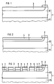
- the polysilicon area arranged under the photoresist mask remains on the surface of the two adjacent trenches 6 and the part of the Si3N4 mask 5 arranged between the two. In this way, a polysilicon web 7 covering both trenches is formed (see FIG. 4).
- the insulation structure 8 comprises lenticular elements, which are each arranged in the upper region of a trench. These lenticular elements of the insulation structure 8 laterally protrude from the respective trench. The length of the protrusion is determined by the thickness of the lenticular element and thus by the duration of the local element Oxidation set.
- the insulation structure comprises an SiO2 web.
- contact holes 9 are formed which extend into the trough 3.
- the contact holes 9 cut through the source regions 4.
- the etching takes place, for. B. with HBr, Ne, O2, NF3.
- the width of the contact holes 9 is set via the thickness of the lenticular oxide structures.
- a contact hole implantation with boron can then be carried out.
- the boron concentration in the tub 3 is increased in the surface of the contact hole 9. This also leads to a change in the p-well structure, which has a favorable effect on the switching behavior of the component.
- Another photo technique opens a further contact hole 10 to the polysilicon web 7 above the polysilicon web 7 (see FIG. 7).
- metallizations 13 are produced in the contact holes 9 and in the contact hole 10.
- the metallizations 13 in the contact holes 9 form a contact between the respective source region 4 and the trough 3.
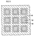
- FIG. 9 shows a section of a MOS cell field that was produced by the method according to the invention.
- the trenches are part of a trench structure 91 which defines square surface elements. Each of the square surface elements is completely surrounded by four trenches.
- the trench structure 91 is filled with doped polysilicon.
- Each of the surface elements comprises along the edge of the trench structure 91 a source region 92 on that facing away from the trench structure 91
- the source region 92 is bounded on each side by a contact 93 which fills a contact hole.
- Each of the surface elements receives a MOS cell.
Landscapes
- Engineering & Computer Science (AREA)
- Microelectronics & Electronic Packaging (AREA)
- Power Engineering (AREA)
- Physics & Mathematics (AREA)
- Ceramic Engineering (AREA)
- Condensed Matter Physics & Semiconductors (AREA)
- General Physics & Mathematics (AREA)
- Computer Hardware Design (AREA)
- Electrodes Of Semiconductors (AREA)
- Insulated Gate Type Field-Effect Transistor (AREA)
- Metal-Oxide And Bipolar Metal-Oxide Semiconductor Integrated Circuits (AREA)
Applications Claiming Priority (2)
| Application Number | Priority Date | Filing Date | Title |
|---|---|---|---|
| DE4300806A DE4300806C1 (de) | 1993-01-14 | 1993-01-14 | Verfahren zur Herstellung von vertikalen MOS-Transistoren |
| DE4300806 | 1993-01-14 |
Publications (2)
| Publication Number | Publication Date |
|---|---|
| EP0609536A2 true EP0609536A2 (fr) | 1994-08-10 |
| EP0609536A3 EP0609536A3 (fr) | 1996-08-14 |
Family
ID=6478187
Family Applications (1)
| Application Number | Title | Priority Date | Filing Date |
|---|---|---|---|
| EP93120324A Withdrawn EP0609536A3 (fr) | 1993-01-14 | 1993-12-16 | Méthode de fabrication de transistors MOS verticaux. |
Country Status (4)
| Country | Link |
|---|---|
| US (1) | US5385852A (fr) |
| EP (1) | EP0609536A3 (fr) |
| JP (1) | JPH07115192A (fr) |
| DE (1) | DE4300806C1 (fr) |
Families Citing this family (41)
| Publication number | Priority date | Publication date | Assignee | Title |
|---|---|---|---|---|
| US6603173B1 (en) | 1991-07-26 | 2003-08-05 | Denso Corporation | Vertical type MOSFET |
| US6015737A (en) * | 1991-07-26 | 2000-01-18 | Denso Corporation | Production method of a vertical type MOSFET |
| EP0675529A3 (fr) * | 1994-03-30 | 1998-06-03 | Denso Corporation | Méthode de fabrication de transistors MOS verticaux |
| US5780324A (en) * | 1994-03-30 | 1998-07-14 | Denso Corporation | Method of manufacturing a vertical semiconductor device |
| US5455190A (en) * | 1994-12-07 | 1995-10-03 | United Microelectronics Corporation | Method of making a vertical channel device using buried source techniques |
| DE19514834C1 (de) * | 1995-04-21 | 1997-01-09 | Siemens Ag | Festwertspeicherzellenanordnung und Verfahren zu deren Herstellung |
| US5589411A (en) * | 1995-07-28 | 1996-12-31 | United Microelectronics Corporation | Process for fabricating a high-voltage MOSFET |
| US6110799A (en) * | 1997-06-30 | 2000-08-29 | Intersil Corporation | Trench contact process |
| US6025260A (en) | 1998-02-05 | 2000-02-15 | Integrated Device Technology, Inc. | Method for fabricating air gap with borderless contact |
| US6503813B1 (en) | 2000-06-16 | 2003-01-07 | International Business Machines Corporation | Method and structure for forming a trench in a semiconductor substrate |
| US7745289B2 (en) | 2000-08-16 | 2010-06-29 | Fairchild Semiconductor Corporation | Method of forming a FET having ultra-low on-resistance and low gate charge |
| US6710403B2 (en) | 2002-07-30 | 2004-03-23 | Fairchild Semiconductor Corporation | Dual trench power MOSFET |
| US6803626B2 (en) | 2002-07-18 | 2004-10-12 | Fairchild Semiconductor Corporation | Vertical charge control semiconductor device |
| US6916745B2 (en) | 2003-05-20 | 2005-07-12 | Fairchild Semiconductor Corporation | Structure and method for forming a trench MOSFET having self-aligned features |
| US6818513B2 (en) | 2001-01-30 | 2004-11-16 | Fairchild Semiconductor Corporation | Method of forming a field effect transistor having a lateral depletion structure |
| GB0122121D0 (en) * | 2001-09-13 | 2001-10-31 | Koninkl Philips Electronics Nv | Edge termination in a trench-gate mosfet |
| GB0122120D0 (en) * | 2001-09-13 | 2001-10-31 | Koninkl Philips Electronics Nv | Edge termination in MOS transistors |
| KR100439189B1 (ko) * | 2001-12-20 | 2004-07-07 | 동부전자 주식회사 | 수직형 트랜지스터 및 그 제조 방법 |
| KR100406578B1 (ko) * | 2001-12-29 | 2003-11-20 | 동부전자 주식회사 | 반도체 소자의 제조방법 |
| US7576388B1 (en) | 2002-10-03 | 2009-08-18 | Fairchild Semiconductor Corporation | Trench-gate LDMOS structures |
| US6710418B1 (en) | 2002-10-11 | 2004-03-23 | Fairchild Semiconductor Corporation | Schottky rectifier with insulation-filled trenches and method of forming the same |
| JP3931138B2 (ja) * | 2002-12-25 | 2007-06-13 | 三菱電機株式会社 | 電力用半導体装置及び電力用半導体装置の製造方法 |
| US7638841B2 (en) | 2003-05-20 | 2009-12-29 | Fairchild Semiconductor Corporation | Power semiconductor devices and methods of manufacture |
| KR100994719B1 (ko) | 2003-11-28 | 2010-11-16 | 페어차일드코리아반도체 주식회사 | 슈퍼정션 반도체장치 |
| US7368777B2 (en) | 2003-12-30 | 2008-05-06 | Fairchild Semiconductor Corporation | Accumulation device with charge balance structure and method of forming the same |
| EP1577952B1 (fr) * | 2004-03-09 | 2018-07-04 | STMicroelectronics Srl | Méthode de fabrication d'un transistor haute tension à effet de champ à grille isolée |
| US7352036B2 (en) | 2004-08-03 | 2008-04-01 | Fairchild Semiconductor Corporation | Semiconductor power device having a top-side drain using a sinker trench |
| TWI237348B (en) * | 2004-08-26 | 2005-08-01 | Mosel Vitelic Inc | Method of manufacturing trench metal oxide semiconductor field effect transistor |
| DE102004057237B4 (de) * | 2004-11-26 | 2007-02-08 | Infineon Technologies Ag | Verfahren zum Herstellen von Kontaktlöchern in einem Halbleiterkörper sowie Transistor mit vertikalem Aufbau |
| WO2006108011A2 (fr) | 2005-04-06 | 2006-10-12 | Fairchild Semiconductor Corporation | Transistors a effet de champ a grille en tranchees, et procedes de creation desdits transistors |
| US7446374B2 (en) | 2006-03-24 | 2008-11-04 | Fairchild Semiconductor Corporation | High density trench FET with integrated Schottky diode and method of manufacture |
| US7319256B1 (en) | 2006-06-19 | 2008-01-15 | Fairchild Semiconductor Corporation | Shielded gate trench FET with the shield and gate electrodes being connected together |
| WO2009039441A1 (fr) | 2007-09-21 | 2009-03-26 | Fairchild Semiconductor Corporation | Structures à superjonction pour dispositifs de puissance et procédés de fabrication |
| US7772668B2 (en) | 2007-12-26 | 2010-08-10 | Fairchild Semiconductor Corporation | Shielded gate trench FET with multiple channels |
| US20120273916A1 (en) | 2011-04-27 | 2012-11-01 | Yedinak Joseph A | Superjunction Structures for Power Devices and Methods of Manufacture |
| US8319290B2 (en) | 2010-06-18 | 2012-11-27 | Fairchild Semiconductor Corporation | Trench MOS barrier schottky rectifier with a planar surface using CMP techniques |
| US8786010B2 (en) | 2011-04-27 | 2014-07-22 | Fairchild Semiconductor Corporation | Superjunction structures for power devices and methods of manufacture |
| US8772868B2 (en) | 2011-04-27 | 2014-07-08 | Fairchild Semiconductor Corporation | Superjunction structures for power devices and methods of manufacture |
| US8836028B2 (en) | 2011-04-27 | 2014-09-16 | Fairchild Semiconductor Corporation | Superjunction structures for power devices and methods of manufacture |
| US8673700B2 (en) | 2011-04-27 | 2014-03-18 | Fairchild Semiconductor Corporation | Superjunction structures for power devices and methods of manufacture |
| CN103534809B (zh) * | 2011-08-05 | 2016-08-17 | 富士电机株式会社 | 半导体器件及半导体器件的制造方法 |
Citations (4)
| Publication number | Priority date | Publication date | Assignee | Title |
|---|---|---|---|---|
| US4967245A (en) * | 1988-03-14 | 1990-10-30 | Siliconix Incorporated | Trench power MOSFET device |
| JPH0311765A (ja) * | 1989-06-09 | 1991-01-21 | Nippon Telegr & Teleph Corp <Ntt> | 半導体装置の製造方法 |
| US5072266A (en) * | 1988-12-27 | 1991-12-10 | Siliconix Incorporated | Trench DMOS power transistor with field-shaping body profile and three-dimensional geometry |
| JPH06232163A (ja) * | 1993-02-05 | 1994-08-19 | Omron Corp | 縦型mosfet装置及びその製造方法 |
Family Cites Families (8)
| Publication number | Priority date | Publication date | Assignee | Title |
|---|---|---|---|---|
| US4191603A (en) * | 1978-05-01 | 1980-03-04 | International Business Machines Corporation | Making semiconductor structure with improved phosphosilicate glass isolation |
| JPS5565463A (en) * | 1978-11-13 | 1980-05-16 | Semiconductor Res Found | Semiconductor device |
| JPS56115525A (en) * | 1980-02-18 | 1981-09-10 | Chiyou Lsi Gijutsu Kenkyu Kumiai | Manufacture of semiconductor device |
| US4983535A (en) * | 1981-10-15 | 1991-01-08 | Siliconix Incorporated | Vertical DMOS transistor fabrication process |
| US4819054A (en) * | 1982-09-29 | 1989-04-04 | Hitachi, Ltd. | Semiconductor IC with dual groove isolation |
| JPS60117613A (ja) * | 1983-11-30 | 1985-06-25 | Fujitsu Ltd | 半導体装置の製造方法 |
| JPH01198076A (ja) * | 1988-02-02 | 1989-08-09 | Mitsubishi Electric Corp | 半導体装置 |
| US5233215A (en) * | 1992-06-08 | 1993-08-03 | North Carolina State University At Raleigh | Silicon carbide power MOSFET with floating field ring and floating field plate |
-
1993
- 1993-01-14 DE DE4300806A patent/DE4300806C1/de not_active Expired - Fee Related
- 1993-12-09 US US08/163,523 patent/US5385852A/en not_active Expired - Fee Related
- 1993-12-16 EP EP93120324A patent/EP0609536A3/fr not_active Withdrawn
-
1994
- 1994-01-11 JP JP6013173A patent/JPH07115192A/ja not_active Withdrawn
Patent Citations (4)
| Publication number | Priority date | Publication date | Assignee | Title |
|---|---|---|---|---|
| US4967245A (en) * | 1988-03-14 | 1990-10-30 | Siliconix Incorporated | Trench power MOSFET device |
| US5072266A (en) * | 1988-12-27 | 1991-12-10 | Siliconix Incorporated | Trench DMOS power transistor with field-shaping body profile and three-dimensional geometry |
| JPH0311765A (ja) * | 1989-06-09 | 1991-01-21 | Nippon Telegr & Teleph Corp <Ntt> | 半導体装置の製造方法 |
| JPH06232163A (ja) * | 1993-02-05 | 1994-08-19 | Omron Corp | 縦型mosfet装置及びその製造方法 |
Non-Patent Citations (5)
| Title |
|---|
| ELECTRONICS LETTERS, 29 AUG. 1991, UK, Bd. 27, Nr. 18, ISSN 0013-5194, Seiten 1640-1642, XP000264480 MATSUMOTO S ET AL: "Ultralow specific on resistance UMOSFET with trench contacts for source and body regions realised by selfaligned process" * |
| IEEE TRANSACTIONS ON ELECTRON DEVICES, APRIL 1987, USA, Bd. ED-34, Nr. 4, ISSN 0018-9383, Seiten 926-930, XP002005720 UEDA D ET AL: "An ultra-low on-resistance power MOSFET fabricated by using a fully self-aligned process" * |
| IEEE TRANSACTIONS ON ELECTRON DEVICES, MAY 1994, USA, Bd. 41, Nr. 5, ISSN 0018-9383, Seiten 814-818, XP000483880 MATSUMOTO S ET AL: "A high-performance self-aligned UMOSFET with a vertical trench contact structure" * |
| PATENT ABSTRACTS OF JAPAN vol. 015, no. 125 (E-1050), 27.März 1991 & JP-A-03 011765 (NIPPON TELEGR & TELEPH CORP), 21.Januar 1991, * |
| PATENT ABSTRACTS OF JAPAN vol. 018, no. 599 (E-1631), 15.November 1994 & JP-A-06 232163 (OMRON CORP), 19.August 1994, * |
Also Published As
| Publication number | Publication date |
|---|---|
| EP0609536A3 (fr) | 1996-08-14 |
| JPH07115192A (ja) | 1995-05-02 |
| US5385852A (en) | 1995-01-31 |
| DE4300806C1 (de) | 1993-12-23 |
Similar Documents
| Publication | Publication Date | Title |
|---|---|---|
| DE4300806C1 (de) | Verfahren zur Herstellung von vertikalen MOS-Transistoren | |
| DE4011276C2 (de) | Feldeffekttransistor mit isoliertem Gate (IGFET) und Verfahren zu seiner Herstellung | |
| DE60132994T2 (de) | Verfahren zur herstellung eines leistungs-mosfets | |
| DE19949364B4 (de) | Halbleiterbauteil mit MOS-Gate-Steuerung und Grabenstruktur sowie Verfahren zur Herstellung | |
| DE10052149B4 (de) | Verfahren zur Herstellung eines Halbleiterbauelements | |
| DE10216633B4 (de) | Halbleiteranordnung und Verfahren zur Herstellung der Halbleiteranordnung | |
| DE69931747T2 (de) | Herstellung eines leistungshalbleiterbauelementes | |
| DE10066412B4 (de) | Halbleiterbauelement und Verfahren zu seiner Herstellung | |
| DE4212861C2 (de) | Feldeffekttransistor und Herstellungsverfahren dafür | |
| DE4235534A1 (de) | Verfahren zum isolieren von fets | |
| EP1138085B1 (fr) | Transistor a effet de champ et son procede de production | |
| DE102011108151A1 (de) | Trench - superjunction - mosfet mit dünnem epi - prozess | |
| DE19535140A1 (de) | Lateraler MOSFET mit hoher Stehspannung und einem Graben sowie Verfahren zu dessen Herstellung | |
| DE2716691A1 (de) | Feldeffekttransistor und verfahren zu dessen herstellung | |
| EP0981155A2 (fr) | Procédé de fabrication d'une couche isolante en semi-conducteur et dispositif semi-conducteur contenant cette couche isolante en semi-conducteur | |
| DE4130555C2 (de) | Halbleitervorrichtung mit hoher Durchbruchsspannung und geringem Widerstand, sowie Herstellungsverfahren | |
| DE3242736A1 (de) | Verfahren zum herstellen feldgesteuerter elemente mit in vertikalen kanaelen versenkten gittern, einschliesslich feldeffekt-transistoren und feldgesteuerten thyristoren | |
| DE4042163A1 (de) | Verfahren zur herstellung einer halbleitervorrichtung | |
| DE19750221B4 (de) | Verfahren zu Herstellung eines Halbleiterbauteils mit MOS-Gatesteuerung | |
| DE3931127C2 (de) | Verfahren zum Herstellen einer Halbleitereinrichtung | |
| DE3421927C2 (de) | Vertikal-MOS-Transistor und Verfahren zu dessen Herstellung | |
| EP1129482A1 (fr) | Procédé de production d'une configuration de cellules DRAM | |
| DE3119137A1 (de) | Halbleiter und verfahren zu deren herstellung | |
| DE69732318T2 (de) | Verfahren zur Herstellung eines bipolaren Transistors | |
| DE102014106747A1 (de) | Halbleitervorrichtung, integrierte schaltung und verfahren zum herstellen einer halbleitervorrichtung |
Legal Events
| Date | Code | Title | Description |
|---|---|---|---|
| PUAI | Public reference made under article 153(3) epc to a published international application that has entered the european phase |
Free format text: ORIGINAL CODE: 0009012 |
|
| AK | Designated contracting states |
Kind code of ref document: A2 Designated state(s): DE FR GB IT |
|
| PUAL | Search report despatched |
Free format text: ORIGINAL CODE: 0009013 |
|
| AK | Designated contracting states |
Kind code of ref document: A3 Designated state(s): DE FR GB IT |
|
| 16A | New documents despatched to applicant after publication of the search report | ||
| STAA | Information on the status of an ep patent application or granted ep patent |
Free format text: STATUS: THE APPLICATION HAS BEEN WITHDRAWN |
|
| 18W | Application withdrawn |
Withdrawal date: 19961203 |