EP0596715B1 - Kontaktbildsensor und Abtastverfahren mittels eines solchen Sensors - Google Patents
Kontaktbildsensor und Abtastverfahren mittels eines solchen Sensors Download PDFInfo
- Publication number
- EP0596715B1 EP0596715B1 EP93308776A EP93308776A EP0596715B1 EP 0596715 B1 EP0596715 B1 EP 0596715B1 EP 93308776 A EP93308776 A EP 93308776A EP 93308776 A EP93308776 A EP 93308776A EP 0596715 B1 EP0596715 B1 EP 0596715B1
- Authority
- EP
- European Patent Office
- Prior art keywords
- reflecting surface
- light
- original
- light source
- image sensor
- Prior art date
- Legal status (The legal status is an assumption and is not a legal conclusion. Google has not performed a legal analysis and makes no representation as to the accuracy of the status listed.)
- Expired - Lifetime
Links
Images


Classifications
-
- H—ELECTRICITY
- H04—ELECTRIC COMMUNICATION TECHNIQUE
- H04N—PICTORIAL COMMUNICATION, e.g. TELEVISION
- H04N1/00—Scanning, transmission or reproduction of documents or the like, e.g. facsimile transmission; Details thereof
-
- H—ELECTRICITY
- H04—ELECTRIC COMMUNICATION TECHNIQUE
- H04N—PICTORIAL COMMUNICATION, e.g. TELEVISION
- H04N1/00—Scanning, transmission or reproduction of documents or the like, e.g. facsimile transmission; Details thereof
- H04N1/024—Details of scanning heads ; Means for illuminating the original
- H04N1/028—Details of scanning heads ; Means for illuminating the original for picture information pick-up
- H04N1/03—Details of scanning heads ; Means for illuminating the original for picture information pick-up with photodetectors arranged in a substantially linear array
- H04N1/031—Details of scanning heads ; Means for illuminating the original for picture information pick-up with photodetectors arranged in a substantially linear array the photodetectors having a one-to-one and optically positive correspondence with the scanned picture elements, e.g. linear contact sensors
- H04N1/0311—Details of scanning heads ; Means for illuminating the original for picture information pick-up with photodetectors arranged in a substantially linear array the photodetectors having a one-to-one and optically positive correspondence with the scanned picture elements, e.g. linear contact sensors using an array of elements to project the scanned image elements onto the photodetectors
- H04N1/0312—Details of scanning heads ; Means for illuminating the original for picture information pick-up with photodetectors arranged in a substantially linear array the photodetectors having a one-to-one and optically positive correspondence with the scanned picture elements, e.g. linear contact sensors using an array of elements to project the scanned image elements onto the photodetectors using an array of optical fibres or rod-lenses
-
- H—ELECTRICITY
- H04—ELECTRIC COMMUNICATION TECHNIQUE
- H04N—PICTORIAL COMMUNICATION, e.g. TELEVISION
- H04N1/00—Scanning, transmission or reproduction of documents or the like, e.g. facsimile transmission; Details thereof
- H04N1/024—Details of scanning heads ; Means for illuminating the original
- H04N1/028—Details of scanning heads ; Means for illuminating the original for picture information pick-up
- H04N1/03—Details of scanning heads ; Means for illuminating the original for picture information pick-up with photodetectors arranged in a substantially linear array
- H04N1/031—Details of scanning heads ; Means for illuminating the original for picture information pick-up with photodetectors arranged in a substantially linear array the photodetectors having a one-to-one and optically positive correspondence with the scanned picture elements, e.g. linear contact sensors
- H04N1/0315—Details of scanning heads ; Means for illuminating the original for picture information pick-up with photodetectors arranged in a substantially linear array the photodetectors having a one-to-one and optically positive correspondence with the scanned picture elements, e.g. linear contact sensors using photodetectors and illumination means mounted on separate supports or substrates or mounted in different planes
-
- H—ELECTRICITY
- H04—ELECTRIC COMMUNICATION TECHNIQUE
- H04N—PICTORIAL COMMUNICATION, e.g. TELEVISION
- H04N1/00—Scanning, transmission or reproduction of documents or the like, e.g. facsimile transmission; Details thereof
- H04N1/024—Details of scanning heads ; Means for illuminating the original
- H04N1/028—Details of scanning heads ; Means for illuminating the original for picture information pick-up
- H04N1/03—Details of scanning heads ; Means for illuminating the original for picture information pick-up with photodetectors arranged in a substantially linear array
- H04N1/031—Details of scanning heads ; Means for illuminating the original for picture information pick-up with photodetectors arranged in a substantially linear array the photodetectors having a one-to-one and optically positive correspondence with the scanned picture elements, e.g. linear contact sensors
- H04N1/0318—Integral pick-up heads, i.e. self-contained heads whose basic elements are a light-source, a lens array and a photodetector array which are supported by a single-piece frame
-
- H—ELECTRICITY
- H04—ELECTRIC COMMUNICATION TECHNIQUE
- H04N—PICTORIAL COMMUNICATION, e.g. TELEVISION
- H04N2201/00—Indexing scheme relating to scanning, transmission or reproduction of documents or the like, and to details thereof
- H04N2201/024—Indexing scheme relating to scanning, transmission or reproduction of documents or the like, and to details thereof deleted
- H04N2201/028—Indexing scheme relating to scanning, transmission or reproduction of documents or the like, and to details thereof deleted for picture information pick-up
- H04N2201/03—Indexing scheme relating to scanning, transmission or reproduction of documents or the like, and to details thereof deleted for picture information pick-up deleted
- H04N2201/031—Indexing scheme relating to scanning, transmission or reproduction of documents or the like, and to details thereof deleted for picture information pick-up deleted deleted
- H04N2201/03104—Integral pick-up heads, i.e. self-contained heads whose basic elements are a light source, a lens and a photodetector supported by a single-piece frame
- H04N2201/03108—Components of integral heads
- H04N2201/03112—Light source
-
- H—ELECTRICITY
- H04—ELECTRIC COMMUNICATION TECHNIQUE
- H04N—PICTORIAL COMMUNICATION, e.g. TELEVISION
- H04N2201/00—Indexing scheme relating to scanning, transmission or reproduction of documents or the like, and to details thereof
- H04N2201/024—Indexing scheme relating to scanning, transmission or reproduction of documents or the like, and to details thereof deleted
- H04N2201/028—Indexing scheme relating to scanning, transmission or reproduction of documents or the like, and to details thereof deleted for picture information pick-up
- H04N2201/03—Indexing scheme relating to scanning, transmission or reproduction of documents or the like, and to details thereof deleted for picture information pick-up deleted
- H04N2201/031—Indexing scheme relating to scanning, transmission or reproduction of documents or the like, and to details thereof deleted for picture information pick-up deleted deleted
- H04N2201/03104—Integral pick-up heads, i.e. self-contained heads whose basic elements are a light source, a lens and a photodetector supported by a single-piece frame
- H04N2201/03108—Components of integral heads
- H04N2201/0312—Reflecting element upstream of the scanned picture elements
-
- H—ELECTRICITY
- H04—ELECTRIC COMMUNICATION TECHNIQUE
- H04N—PICTORIAL COMMUNICATION, e.g. TELEVISION
- H04N2201/00—Indexing scheme relating to scanning, transmission or reproduction of documents or the like, and to details thereof
- H04N2201/024—Indexing scheme relating to scanning, transmission or reproduction of documents or the like, and to details thereof deleted
- H04N2201/028—Indexing scheme relating to scanning, transmission or reproduction of documents or the like, and to details thereof deleted for picture information pick-up
- H04N2201/03—Indexing scheme relating to scanning, transmission or reproduction of documents or the like, and to details thereof deleted for picture information pick-up deleted
- H04N2201/031—Indexing scheme relating to scanning, transmission or reproduction of documents or the like, and to details thereof deleted for picture information pick-up deleted deleted
- H04N2201/03104—Integral pick-up heads, i.e. self-contained heads whose basic elements are a light source, a lens and a photodetector supported by a single-piece frame
- H04N2201/03108—Components of integral heads
- H04N2201/03129—Transparent cover or transparent document support mounted on the head
-
- H—ELECTRICITY
- H04—ELECTRIC COMMUNICATION TECHNIQUE
- H04N—PICTORIAL COMMUNICATION, e.g. TELEVISION
- H04N2201/00—Indexing scheme relating to scanning, transmission or reproduction of documents or the like, and to details thereof
- H04N2201/024—Indexing scheme relating to scanning, transmission or reproduction of documents or the like, and to details thereof deleted
- H04N2201/028—Indexing scheme relating to scanning, transmission or reproduction of documents or the like, and to details thereof deleted for picture information pick-up
- H04N2201/03—Indexing scheme relating to scanning, transmission or reproduction of documents or the like, and to details thereof deleted for picture information pick-up deleted
- H04N2201/031—Indexing scheme relating to scanning, transmission or reproduction of documents or the like, and to details thereof deleted for picture information pick-up deleted deleted
- H04N2201/03104—Integral pick-up heads, i.e. self-contained heads whose basic elements are a light source, a lens and a photodetector supported by a single-piece frame
- H04N2201/03108—Components of integral heads
- H04N2201/03133—Window, i.e. a transparent member mounted in the frame
-
- H—ELECTRICITY
- H04—ELECTRIC COMMUNICATION TECHNIQUE
- H04N—PICTORIAL COMMUNICATION, e.g. TELEVISION
- H04N2201/00—Indexing scheme relating to scanning, transmission or reproduction of documents or the like, and to details thereof
- H04N2201/024—Indexing scheme relating to scanning, transmission or reproduction of documents or the like, and to details thereof deleted
- H04N2201/028—Indexing scheme relating to scanning, transmission or reproduction of documents or the like, and to details thereof deleted for picture information pick-up
- H04N2201/03—Indexing scheme relating to scanning, transmission or reproduction of documents or the like, and to details thereof deleted for picture information pick-up deleted
- H04N2201/031—Indexing scheme relating to scanning, transmission or reproduction of documents or the like, and to details thereof deleted for picture information pick-up deleted deleted
- H04N2201/03104—Integral pick-up heads, i.e. self-contained heads whose basic elements are a light source, a lens and a photodetector supported by a single-piece frame
- H04N2201/03108—Components of integral heads
- H04N2201/03141—Photodetector lens
-
- H—ELECTRICITY
- H04—ELECTRIC COMMUNICATION TECHNIQUE
- H04N—PICTORIAL COMMUNICATION, e.g. TELEVISION
- H04N2201/00—Indexing scheme relating to scanning, transmission or reproduction of documents or the like, and to details thereof
- H04N2201/024—Indexing scheme relating to scanning, transmission or reproduction of documents or the like, and to details thereof deleted
- H04N2201/028—Indexing scheme relating to scanning, transmission or reproduction of documents or the like, and to details thereof deleted for picture information pick-up
- H04N2201/03—Indexing scheme relating to scanning, transmission or reproduction of documents or the like, and to details thereof deleted for picture information pick-up deleted
- H04N2201/031—Indexing scheme relating to scanning, transmission or reproduction of documents or the like, and to details thereof deleted for picture information pick-up deleted deleted
- H04N2201/03104—Integral pick-up heads, i.e. self-contained heads whose basic elements are a light source, a lens and a photodetector supported by a single-piece frame
- H04N2201/03108—Components of integral heads
- H04N2201/03145—Photodetector
-
- H—ELECTRICITY
- H04—ELECTRIC COMMUNICATION TECHNIQUE
- H04N—PICTORIAL COMMUNICATION, e.g. TELEVISION
- H04N2201/00—Indexing scheme relating to scanning, transmission or reproduction of documents or the like, and to details thereof
- H04N2201/024—Indexing scheme relating to scanning, transmission or reproduction of documents or the like, and to details thereof deleted
- H04N2201/028—Indexing scheme relating to scanning, transmission or reproduction of documents or the like, and to details thereof deleted for picture information pick-up
- H04N2201/03—Indexing scheme relating to scanning, transmission or reproduction of documents or the like, and to details thereof deleted for picture information pick-up deleted
- H04N2201/031—Indexing scheme relating to scanning, transmission or reproduction of documents or the like, and to details thereof deleted for picture information pick-up deleted deleted
- H04N2201/03104—Integral pick-up heads, i.e. self-contained heads whose basic elements are a light source, a lens and a photodetector supported by a single-piece frame
- H04N2201/0315—Details of integral heads not otherwise provided for
- H04N2201/03175—Position
Definitions
- the present invention relates to a contact type image sensor and, more particularly, to a contact type image sensor comprising a light source for emitting the light with a predetermined inclination angle in the direction of a normal line of the surface of an original locating at the position of a read line, an original supporting member for leading the light from the light source to the read line and for supporting the original; and a photoelectric converting device section to receive the light from the original surface.
- the invention also concerns a method of sensing by means of said sensor.
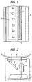
- Fig. 1 is a plan view showing an example of a construction of the conventional contact type image sensor.
- Fig. 2 is a cross sectional view of Fig. 1.
- the contact type image sensor of the constructional example comprises: an LED array 3 in which a plurality of LED devices 2 to irradiate lights to an original 8 are arranged in correspondence to an original read line 9 of the upper surface of a cover glass 6 as an original supporting member so as to have a length corresponding to a width of original 8 to be read; a lens array 1 to lead the reflected lights from the original 8; a sensor array 5 which is constructed by arranging photoelectric converting devices 4 for receiving the light directed by the lens array 1 and for converting into the electric signals; and a frame body 7 to position the above component elements.
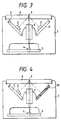
- a contact type image sensor with a constructional example as shown in Fig. 3 is used as a sensor to read the original having concave and convex portions.
- the contact type image sensor of the present constructional example by symmetrically arranging the LED arrays 3 and 3' on both sides for the read line 9 with respect to the left and right, the occurrence of the shadows is prevented.
- a contact type image sensor with a constructional example as shown in Fig. 4 has been proposed.
- the LED array 3' in Fig. 3 is eliminated and a mirror 10 is arranged at the position corresponding to the LED array 3', the reflected light from the original by the LED array 3 is received, and the reflected light is reflected and is again returned to the original, thereby obtaining an effect similar to that in case of the construction of Fig. 3 and reducing the costs.
- the reflected light amount of the mirror 10 depends on the reflected light amount of the original, the reflected light amount of the mirror is largely fluctuated due to a reflection density of the original. Particularly, in case of reading the original of a large density, the reflected light amount is small and a sufficient effect cannot be obtained.
- the present invention seeks to provide an improved contact type image sensor.
- a contact type image sensor for sensing an original, the sensor comprising;
- the illuminance on the original surface at the read line position by the light that is directly irradiated from the light source is the same as the illuminance on the original surface at the read line position by the light that is reflected by the reflecting surface.
- Fig. 5 is a cross sectional view showing a contact type image sensor of the first embodiment according to the invention.
- the same component elements as those shown in Figs. 1 to 4 are designated by the same reference numerals.
- reference numeral 5 denotes the sensor array which is constructed by arranging a plurality of photoelectric converting devices 4 in correspondence to the width of original.
- the sensor array 5 is arranged in an elongated space of the frame body 7.
- the lens array 1 is arranged in a groove of the frame body 7 just above the photoelectric converting devices 4.
- the LED array 3 which is constructed by arranging a plurality of LED devices 2 is arranged as a light source onto a slant surface 3' having an inclination angle of 45° formed on the frame body 7.
- the cover glass 6 for supporting the original is arranged on the upper surface of the frame body 7 and lens array 1. To precisely position the cover glass 6, a cover glass confronting surface 12 is provided for the frame body 7.
- the LED array 3 is arranged on one side and a side surface 11 of the cover glass 6 is arranged on the opposite side at the position close to the read line 9 so as to sandwich the original read line 9 of the cover glass 6.
- the side surface 11 is used as a reflecting surface for reflecting a part of the light of the LED array 3 as a light source and for leading the light from the direction opposite to the light source to the read line 9.
- the reflecting surface of the cover glass 6 is worked by an ordinary cheap glass cutting working technique such that the surface is scratched by a diamond cutter and is cut out or by using a dicing saw, processing by a razor, or the like.
- the illuminance on the original read line 9 is increased by 1.5 times or more and a sufficient effect is obtained as a reflecting surface.
- the scattering of the light is prevented and the illuminance on the original read line can be raised by a value near 2.0 times.
- a stairway-like shape can be formed as shown in the second embodiment of Fig. 6 or a groove can be also formed.
- the cover glass is made thick and is closely adhered to the lens array 1 in order to enable the cover glass to be easily attached.
- a similar effect can be also similarly obtained even by a structure such that the lens array 1 is away from the cover glass 6.
- the LED array has been used as a light source, it is also possible to use another light source such as fluorescent lamp, a xenon lamp, EL light source, or the like.
- a contact type image sensor of the third embodiment of the invention will now be described.
- Fig. 7 is a cross sectional view showing the contact type image sensor of the third embodiment of the invention.
- the LED array 3 in which the LED devices 2 as point light sources are discretely arranged in a line has been used as a light source.
- a fluctuation occurs in the illuminance on the original surface due to a ripple corresponding to the interval between the LED chips and there is a case where such an illuminance fluctuation appears as an output image.
- the illuminance fluctuation is further enhanced when the side surface 11 as a reflecting surface is provided for the cover glass.
- the side surface as a reflecting surface to a scattering surface 13
- the illuminance fluctuation due to the ripple of the point light source in case of using a point light source array is reduced.
- the scattering surface can be obtained by a simple working method such that convex and concave surfaces are formed by a sand blast or chemical process or a scattering paint is coated or the like.
- Figs. 8 to 12 show constructional examples of the fourth to eighth embodiments of the shapes of the cover glasses as original supporting members in the first and second embodiments described above.
- Fig. 8 shows the fourth embodiment in which the original supporting member is divided into two portions and they are adhered by an adhesive agent 14 in order to enable the side surface 11 as a reflecting surface in Fig. 6 to be easily polished. Those two portions of the original supporting member can be also overlaid and fixed to the frame body 7, respectively, without using the adhesive agent 14.
- Fig. 9 shows the fifth embodiment in which the reflecting surface is provided by forming a groove onto the original supporting member by a dicing saw or the like.
- reference numeral 15 denotes a groove formed.
- One side surface 11 of the groove 15 is used as a reflecting surface.
- Figs. 10 and 11 show the sixth and seventh embodiments in which a light transparency plate member 16 is adhered onto the original supporting member through an adhesive agent in order to smoothly pass the original without any click.
- the shapes of the cover glasses in Figs. 10 and 11 correspond to the shapes of the cover glasses in Figs. 6 and 5.
- the edge surface of the cover glass 6 is located near (right side in Fig. 5) of the read line 9 and, further, a cover glass 6' which is come into contact with the edge surface and has the same thickness as that of the edge surface can be also arranged.
- a hooking of the original can be eliminated.
- the foregoing reflecting surface of scattering surface can be formed.
- At least a part of the original supporting member locating on the side opposite to the arrangement side of the light source with respect to the read line is equipped with the reflecting surface or diffusing surface for reflecting a part of the light from the light source and for leading to the read line, so that the light can be irradiated from both sides to the read line by one light source.
- the reflecting surface to a total reflection angle for the light of the light source or to the mirror surface, it is possible to obtain a predetermined illuminance irrespective of the reflection density of the original and the characteristics such that the shadows of the original having concave and convex portions like an original such that papers are adhered onto a base paper which are almost similar to those in case of the conventional contact type image sensor in which the light sources are provided on both sides so as to sandwich the read line.
- the size and costs can be also reduced.
- the invention can also correspond to the contact type image sensor which can read an original image at a high speed and a high resolution.
- the illuminance fluctuation corresponding to the ripple of the point light source can be reduced.
- Fig. 13 is a cross sectional view of the ninth embodiment of the contact type image sensor of the invention and shows the typical feature of the invention.
- Reference numeral 17 denotes a lens to adjust the position of an optical axis Y of the illumination light from the LED array 2.
- the light irradiated from the LED array 2 passes along optical paths A and B in Fig. 13 and reaches a reading position X.
- the illuminance on the original surface by the direct irradiation light at the reading position X and the illuminance on the original surface by the reflected light from the reflecting surface is set to 1 : 1.
- Fig. 14 is a partial enlarged diagram of Fig. 13 showing the optical paths A and B and a virtual optical path B'.
- Fig. 15 is a graph showing an illumination distribution on the original supporting member in the case where the system doesn't have reflecting surface.
- B' denotes the virtual optical axis in case of no reflecting surface and X' indicates a virtual reading position. It is assumed that the illuminance at the virtual reading position X' is equal to the illuminance at the reading position X by the light which has reached by the optical path B.
- the illuminance distribution on the original supporting member can be set to a distribution as shown by a solid line in Fig. 15.
- botn of the illuminance at the reading position X and the illuminance at the virtual reading position X' are equal to y 2 . That is, the illuminance on the reading position X by the light which reaches the reading position X from the optical path A is equal to the illuminance on the reading position X by the light which reaches the reading position X from the optical path B.
- the amount of light which passes along the optical path A and reaches the original reading position X can be almost equalized to the amount of light which passes along the optical path B and reaches the original reading position X.
- the illuminance on the original surface by the direct irradiation light at the reading position X and the illuminance on the original surface by the reflected light from the reflecting surface are set to almost 1 : 1.
- the lens 17 has been used to adjust the optical axis Y.
- the optical axis Y can be also adjusted by changing the attaching angle of the substrate of the LED array or a package shape of the LED chip.
- the optical axis Y has been arranged to the position (position Z in the diagram) on the reflecting surface, the invention is not limited to such a position. It is sufficient to arrange the optical axis Y to a proper position (region a in the diagram) between the reading position X and the reflecting surface or on the reflecting surface (region b in the diagram) in accordance with the directing characteristics of the LED array, a refractive index of the reflecting surface, or the like.
- the ninth embodiment of the invention in case of using the contact type image sensor using both of the direct irradiation light from the light source and the reflected light from the reflecting surface of the original supporting member, by arranging the optical axis of the illumination light from the light source to a region between the read line and the reflecting surface or onto the reflecting surface, the light amount ratio at the read line positions of both of the optical paths can be set to almost 1 : 1. Consequently, since the effect to erase the shadows which are formed around the concave and convex portions of the original can be maximized. The using efficiency of the light from the light source is also improved. The light amount at the read line position is doubled. The burden on the light source is decreased.
- the contact type image sensor of a high picture quality having substantially the same performance as that of the type using two LED arrays as shown in Fig. 3 can be realized by a smaller size and at lower costs. An electric power consumption of the light source can be also suppressed. Further, a contact type image sensor which can correspond to the driving of the sensor at a higher speed can be provided.
- the above effect can be also accomplished by using a light source of an LED array or the like having gentle directing characteristics as a light source.
- a light source of an LED array or the like having gentle directing characteristics as a light source.
- an attaching margin of the light source ensures a construction such that the system can be easily assembled.
Landscapes
- Engineering & Computer Science (AREA)
- Multimedia (AREA)
- Signal Processing (AREA)
- Facsimile Heads (AREA)
- Facsimile Scanning Arrangements (AREA)
Claims (18)
- Kontaktbildsensor zum Erfassen eines Originals (8) mit folgendem:dadurch gekennzeichnet, daß(a) einem Original-Stützelement (6), um das Original zu stützen, wobei das Original-Stützelement ein lichtdurchlässiges Element (6) hat, um mit dem Original an einer Leseposition (9) in Kontakt zu stehen und eine Bildebene zu definieren, in der sich das Original an der Leseposition im Gebrauch erstreckt;(b) einer Lichtquelle (2), die eingerichtet ist, um eine Beleuchtung an der Leseposition in der Bildebene mittels eines Lichts vorzusehen, das durch das lichtdurchlässige Element in einer ersten Richtung mit einem vorbestimmten Neigungswinkel gegenüber einer Linie gerichtet ist, die an der Leseposition normal zu der Bildebene ist,;(c) einer photoelektrischen Umwandlungsvorrichtung (4), die betreibbar ist, um Licht von dem Original zu empfangen, wenn es im Gebrauch an der Leseposition durch ein Licht von der Lichtquelle beleuchtet wird; und(d) einer Reflexionsfläche (11), die derart angeordnet ist, daß die Lichtquelle und die Reflexionsfläche auf entgegengesetzten Seiten der Linie sind, die an der Leseposition normal zu der Bildebene ist, und derart, daß ein Teil des Lichts von der Lichtquelle durch die Reflexionsfläche reflektiert wird, um eine weitere Beleuchtung an der Leseposition in einer von der ersten Richtung verschiedenen zweiten Richtung vorzusehen;
die Reflexionsfläche durch eine Fläche (11) des lichtdurchlässigen Elements ausgebildet und in einer derartigen Weise eingerichtet ist, daß der Teil des Lichts von der Lichtquelle in der Lage ist, direkt auf die Reflexionsfläche einzufallen, ohne auf seinem Weg von der Lichtquelle zu der Reflexionsfläche durch eine andere Fläche reflektiert zu werden. - Bildsensor nach Anspruch 1, wobei das lichtdurchlässige Element aus Glas gefertigt ist und wobei die Reflexionsfläche durch eine Glas-Luft-Grenzfläche gebildet ist, die eine Reflexion durch eine innere Reflexion an der Grenzfläche vorsieht.
- Bildsensor nach Anspruch 1, wobei ein Winkel des Lichteinfalls von der Lichtquelle auf die Reflexionsfläche auf einen Winkel eingestellt ist, der gleich oder größer als ein kritischer Winkel (Θh) ist, der sich aufgrund einer Differenz des Brechungsindex über eine die Reflexionsfläche definierende Grenzschicht ergibt.
- Bildsensor nach einem der vorangehenden Ansprüche, wobei die Reflexionsfläche poliert ist.
- Bildsensor nach Anspruch 1, wobei die Reflexionsfläche eine Spiegelfläche ist.
- Bildsensor nach einem der Ansprüche 1 bis 3, wobei die Reflexionsfläche eine Streufläche (13 in Fig. 7) ist.
- Bildsensor nach einem der vorangehenden Ansprüche, wobei die Reflexionsfläche durch eine Endfläche des lichtdurchlässigen Elements definiert ist.
- Bildsensor nach einem der Ansprüche 1 bis 6, wobei die Reflexionsfläche (11 in Fig. 6) durch eine Stufenausbildung des lichtdurchlässigen Elements definiert ist.
- Bildsensor nach einem der Ansprüche 1 bis 6, wobei die Reflexionsfläche durch eine Seitenwand einer in dem lichtdurchlässigen Element ausgebildeten Nut (15 in Fig. 9) definiert ist.
- Bildsensor nach einem der vorangehenden Ansprüche, wobei das Original-Stützelement das lichtdurchlässige Element (6) aufweist, das mit einem Plattenelement (16 in den Figuren 10-12) überzogen ist, um mit dem Original in Kontakt zu stehen.
- Bildsensor nach einem der vorangehenden Ansprüche, wobei sich die Leseposition linear über die Bildebene erstreckt und wobei die Reflexionsfläche durch eine sich parallel zu der linearen Ausdehnung der Leseposition erstreckende ebene Fläche definiert ist.
- Verfahren zum Abtasten eines Originals (8) mittels eines Kontaktbildsensors, mit den Schritten:dadurch gekennzeichnet, daß(a) Stützen eines Originals mittels eines Original-Stützelements (6), das ein lichtdurchlässiges Element (6) hat, das mit dem Original an einer Leseposition (9) in Kontakt steht und eine Bildebene definiert, in der sich das Original an der Leseposition im Gebrauch erstreckt;(b) Gewährleisten einer Beleuchtung an der Leseposition in der Bildebene mittels eines Lichts, das von einer Lichtquelle (2) durch das lichtdurchlässige Element in einer ersten Richtung mit einem vorbestimmten Neigungswinkel gegenüber einer Linie gerichtet ist, die an der Leseposition normal zu der Bildebene ist;(c) photoelektrisches Umwandeln von Licht, das von dem Original empfangen wird, wenn es bei einer Benutzung an der Leseposition durch ein Licht von der Lichtquelle beleuchtet wird; und(d) Vorsehen einer weiteren Beleuchtung in einer von der ersten Richtung verschiedenen zweiten Richtung durch Reflektieren eines Teils des Lichts von der Lichtquelle durch eine Reflexionsfläche (11), die derart angeordnet ist, daß die Lichtquelle und die Reflexionsfläche auf entgegengesetzten Seiten der Linie sind, die an der Leseposition normal zu der Bildebene ist;
die Reflexionsfläche durch eine Fläche (11) des lichtdurchlässigen Elements ausgebildet und die weitere Beleuchtung derart vorgesehen ist, daß der Teil des Lichts von der Lichtquelle direkt auf die Reflexionsfläche einfällt, ohne auf dessen Weg von der Lichtquelle zu der Reflexionsfläche durch eine andere Fläche reflektiert zu werden. - Verfahren nach Anspruch 12, wobei das lichtdurchlässige Element aus Glas gefertigt ist und wobei das Licht an der Reflexionsfläche durch eine Glas-Luft-Grenzfläche reflektiert wird, die eine Reflexion durch eine innere Reflexion an der Grenzfläche vorsieht.
- Verfahren nach Anspruch 12, wobei ein Winkel des Lichteinfalls von der Lichtquelle auf die Reflexionsfläche auf einen Winkel eingestellt ist, der gleich oder größer als ein kritischer Winkel (Θh) ist, der sich aufgrund einer Differenz des Brechungsindex über eine die Reflexionsfläche definierende Grenzschicht ergibt.
- Verfahren nach einem der Ansprüche 12 bis 14, wobei eine spiegelnde Reflexion an der Reflexionsfläche auftritt, die poliert ist.
- Verfahren nach Anspruch 12 wobei eine spiegelnde Reflexion an der Reflexionsfläche auftritt, die eine Spiegelfläche ist.
- Verfahren nach einem der Ansprüche 12 bis 14, wobei eine diffuse Reflexion an der Reflexionsfläche auftritt, die eine Streufläche ist.
- Verfahren nach einem der Ansprüche 12 bis 17, wobei sich die Leseposition linear über die Bildebene erstreckt und wobei die Reflexionsfläche durch eine sich parallel zu der linearen Ausdehnung der Leseposition erstreckende ebene Fläche definiert ist.
Applications Claiming Priority (6)
| Application Number | Priority Date | Filing Date | Title |
|---|---|---|---|
| JP31801592 | 1992-11-04 | ||
| JP318015/92 | 1992-11-04 | ||
| JP4318015A JP2946447B2 (ja) | 1992-11-04 | 1992-11-04 | 密着型イメージセンサー |
| JP10598493 | 1993-04-09 | ||
| JP05105984A JP3080810B2 (ja) | 1993-04-09 | 1993-04-09 | 密着型イメージセンサー |
| JP105984/93 | 1993-04-09 |
Publications (2)
| Publication Number | Publication Date |
|---|---|
| EP0596715A1 EP0596715A1 (de) | 1994-05-11 |
| EP0596715B1 true EP0596715B1 (de) | 1999-06-16 |
Family
ID=26446198
Family Applications (1)
| Application Number | Title | Priority Date | Filing Date |
|---|---|---|---|
| EP93308776A Expired - Lifetime EP0596715B1 (de) | 1992-11-04 | 1993-11-03 | Kontaktbildsensor und Abtastverfahren mittels eines solchen Sensors |
Country Status (4)
| Country | Link |
|---|---|
| US (1) | US5357099A (de) |
| EP (1) | EP0596715B1 (de) |
| KR (1) | KR970006788B1 (de) |
| DE (1) | DE69325337T2 (de) |
Cited By (3)
| Publication number | Priority date | Publication date | Assignee | Title |
|---|---|---|---|---|
| DE10123870A1 (de) * | 2001-05-16 | 2003-05-15 | Opdi Tex Gmbh | Vorrichtung zur automatischen Überwachung von Flächengebilden, insbesondere textilen Gewebebahnen an der Produktionsmaschine |
| DE19921358B4 (de) * | 1999-05-10 | 2005-07-14 | Profichip Gmbh | Parametrierbares, kaskadierbares Filter |
| EP1041807B1 (de) * | 1999-03-31 | 2009-12-02 | Hewlett-Packard Company, A Delaware Corporation | Integriertes optisches Bildgerät |
Families Citing this family (11)
| Publication number | Priority date | Publication date | Assignee | Title |
|---|---|---|---|---|
| JP2784138B2 (ja) * | 1993-12-09 | 1998-08-06 | 三菱電機株式会社 | イメージセンサ |
| JPH09219768A (ja) * | 1996-02-09 | 1997-08-19 | Canon Inc | イメージセンサ |
| JPH1012915A (ja) * | 1996-06-26 | 1998-01-16 | Oki Electric Ind Co Ltd | 光学式パターン読取りセンサ |
| JPH10190946A (ja) * | 1996-12-27 | 1998-07-21 | Canon Inc | 密着型イメージセンサとこれを用いた画像読み取り装置 |
| DE19715760A1 (de) * | 1997-04-16 | 1998-10-22 | Einighammer Hans J Dr | Verfahren zur Abbildung mit großem Gesichtsfeld mittels kleiner Optik und Vorrichtung zur Durchführung des Verfahrens |
| JPH11284796A (ja) * | 1998-03-30 | 1999-10-15 | Mitsubishi Electric Corp | イメージセンサ |
| EP1624667A2 (de) * | 1998-12-24 | 2006-02-08 | Canon Kabushiki Kaisha | Beleuchtungs-Gerät mit Benutzung von Lichtleitern |
| JP4168960B2 (ja) * | 2004-03-24 | 2008-10-22 | 富士ゼロックス株式会社 | 画像読み取り装置、画像読み取りユニット、光照射装置 |
| JP2007214948A (ja) * | 2006-02-10 | 2007-08-23 | Canon Inc | 画像読取装置 |
| JP5087337B2 (ja) * | 2007-07-25 | 2012-12-05 | スタンレー電気株式会社 | 原稿読取用光源装置 |
| KR102817003B1 (ko) | 2024-08-22 | 2025-06-05 | 주식회사 에프에이에스 | 2.5차원 이미지 스캔용 밀착형 이미지 센서 |
Family Cites Families (9)
| Publication number | Priority date | Publication date | Assignee | Title |
|---|---|---|---|---|
| JPS5840972A (ja) * | 1981-09-04 | 1983-03-10 | Fujitsu Ltd | 原稿読取装置の構成 |
| JPS58143665A (ja) * | 1982-02-19 | 1983-08-26 | Fuji Xerox Co Ltd | 密着型読取装置 |
| US5196950A (en) * | 1988-08-04 | 1993-03-23 | Ricoh Company, Ltd. | Optical reader and light source used for the same |
| DE8906063U1 (de) * | 1989-05-12 | 1989-07-13 | Siemens AG, 1000 Berlin und 8000 München | Optische Abtastvorrichtung mit einem Bündel von lichtleitenden Fasern |
| JP2744307B2 (ja) * | 1989-11-21 | 1998-04-28 | キヤノン株式会社 | 光電変換装置 |
| US5142137A (en) * | 1990-05-18 | 1992-08-25 | Sharp Kabushiki Kaisha | Image sensor having clamp connecting sensing and driving components |
| JPH0470053A (ja) * | 1990-07-09 | 1992-03-05 | Mitsubishi Electric Corp | 密着型イメージセンサ |
| US5130761A (en) * | 1990-07-17 | 1992-07-14 | Kabushiki Kaisha Toshiba | Led array with reflector and printed circuit board |
| JPH05304318A (ja) * | 1992-02-06 | 1993-11-16 | Rohm Co Ltd | 発光素子アレイ基板 |
-
1993
- 1993-11-03 EP EP93308776A patent/EP0596715B1/de not_active Expired - Lifetime
- 1993-11-03 US US08/145,234 patent/US5357099A/en not_active Expired - Lifetime
- 1993-11-03 KR KR1019930023178A patent/KR970006788B1/ko not_active Expired - Fee Related
- 1993-11-03 DE DE69325337T patent/DE69325337T2/de not_active Expired - Fee Related
Cited By (3)
| Publication number | Priority date | Publication date | Assignee | Title |
|---|---|---|---|---|
| EP1041807B1 (de) * | 1999-03-31 | 2009-12-02 | Hewlett-Packard Company, A Delaware Corporation | Integriertes optisches Bildgerät |
| DE19921358B4 (de) * | 1999-05-10 | 2005-07-14 | Profichip Gmbh | Parametrierbares, kaskadierbares Filter |
| DE10123870A1 (de) * | 2001-05-16 | 2003-05-15 | Opdi Tex Gmbh | Vorrichtung zur automatischen Überwachung von Flächengebilden, insbesondere textilen Gewebebahnen an der Produktionsmaschine |
Also Published As
| Publication number | Publication date |
|---|---|
| KR970006788B1 (ko) | 1997-04-30 |
| KR940013109A (ko) | 1994-06-25 |
| DE69325337T2 (de) | 1999-11-18 |
| DE69325337D1 (de) | 1999-07-22 |
| EP0596715A1 (de) | 1994-05-11 |
| US5357099A (en) | 1994-10-18 |
Similar Documents
| Publication | Publication Date | Title |
|---|---|---|
| EP0596715B1 (de) | Kontaktbildsensor und Abtastverfahren mittels eines solchen Sensors | |
| US6724503B1 (en) | Image sensor substrate and image sensor employing it | |
| US6767122B2 (en) | Light guide, line illumination apparatus, and image acquisition system | |
| JP3688832B2 (ja) | 線状光源装置、これに用いる導光部材、およびこの導光部材を用いた線状光源を備える画像読み取り装置 | |
| KR0158247B1 (ko) | 도광체와, 이 도광체를 갖는 조명 장치, 그리고 이 조명 장치를 갖는 화상 판독장치 및 정보 처리 장치 | |
| EP1104163B1 (de) | Lineare Beleuchtungseinrichtung | |
| EP0560605B1 (de) | Lichtquelle | |
| US5696607A (en) | Image reader having a light-guiding transparent board | |
| US5585615A (en) | Image reading apparatus | |
| EP2811221B1 (de) | Bestrahlungsvorrichtung und bildlesevorrichtung | |
| TW200427303A (en) | Image reading device | |
| US6744033B2 (en) | Bar-shaped light guide, line-illuminating device incorporated with the bar-shaped light guide and contact-type image sensor incorporated with the line-illuminating device | |
| US7942561B2 (en) | Light guide having reflective protruding portion, and lighting devices including such light guide | |
| US6081351A (en) | Image reading apparatus | |
| JP2725650B2 (ja) | Ledアレイ光源 | |
| JP2892812B2 (ja) | 半導体レーザ装置 | |
| JP4096421B2 (ja) | 画像読み取り装置 | |
| JP2946447B2 (ja) | 密着型イメージセンサー | |
| JP3068717B2 (ja) | 画像読取装置 | |
| JP3086063B2 (ja) | 密着型イメージセンサ | |
| JPH11261172A (ja) | 半導体レーザ装置 | |
| JP3307978B2 (ja) | イメージセンサ | |
| JP2539478Y2 (ja) | 原稿読み取り装置 | |
| JPS63214058A (ja) | 密着イメ−ジセンサ | |
| JPH04168434A (ja) | 原稿照明装置 |
Legal Events
| Date | Code | Title | Description |
|---|---|---|---|
| PUAI | Public reference made under article 153(3) epc to a published international application that has entered the european phase |
Free format text: ORIGINAL CODE: 0009012 |
|
| AK | Designated contracting states |
Kind code of ref document: A1 Designated state(s): DE FR GB IT NL |
|
| 17P | Request for examination filed |
Effective date: 19940923 |
|
| 17Q | First examination report despatched |
Effective date: 19970429 |
|
| GRAG | Despatch of communication of intention to grant |
Free format text: ORIGINAL CODE: EPIDOS AGRA |
|
| GRAG | Despatch of communication of intention to grant |
Free format text: ORIGINAL CODE: EPIDOS AGRA |
|
| GRAH | Despatch of communication of intention to grant a patent |
Free format text: ORIGINAL CODE: EPIDOS IGRA |
|
| GRAH | Despatch of communication of intention to grant a patent |
Free format text: ORIGINAL CODE: EPIDOS IGRA |
|
| GRAH | Despatch of communication of intention to grant a patent |
Free format text: ORIGINAL CODE: EPIDOS IGRA |
|
| GRAA | (expected) grant |
Free format text: ORIGINAL CODE: 0009210 |
|
| AK | Designated contracting states |
Kind code of ref document: B1 Designated state(s): DE FR GB IT NL |
|
| PG25 | Lapsed in a contracting state [announced via postgrant information from national office to epo] |
Ref country code: NL Free format text: LAPSE BECAUSE OF FAILURE TO SUBMIT A TRANSLATION OF THE DESCRIPTION OR TO PAY THE FEE WITHIN THE PRESCRIBED TIME-LIMIT Effective date: 19990616 Ref country code: IT Free format text: LAPSE BECAUSE OF FAILURE TO SUBMIT A TRANSLATION OF THE DESCRIPTION OR TO PAY THE FEE WITHIN THE PRE;WARNING: LAPSES OF ITALIAN PATENTS WITH EFFECTIVE DATE BEFORE 2007 MAY HAVE OCCURRED AT ANY TIME BEFORE 2007. THE CORRECT EFFECTIVE DATE MAY BE DIFFERENT FROM THE ONE RECORDED.SCRIBED TIME-LIMIT Effective date: 19990616 |
|
| REF | Corresponds to: |
Ref document number: 69325337 Country of ref document: DE Date of ref document: 19990722 |
|
| ET | Fr: translation filed | ||
| NLV1 | Nl: lapsed or annulled due to failure to fulfill the requirements of art. 29p and 29m of the patents act | ||
| PLBE | No opposition filed within time limit |
Free format text: ORIGINAL CODE: 0009261 |
|
| 26N | No opposition filed | ||
| REG | Reference to a national code |
Ref country code: GB Ref legal event code: IF02 |
|
| PGFP | Annual fee paid to national office [announced via postgrant information from national office to epo] |
Ref country code: GB Payment date: 20051021 Year of fee payment: 13 |
|
| PGFP | Annual fee paid to national office [announced via postgrant information from national office to epo] |
Ref country code: FR Payment date: 20051116 Year of fee payment: 13 |
|
| PGFP | Annual fee paid to national office [announced via postgrant information from national office to epo] |
Ref country code: DE Payment date: 20060125 Year of fee payment: 13 |
|
| PG25 | Lapsed in a contracting state [announced via postgrant information from national office to epo] |
Ref country code: DE Free format text: LAPSE BECAUSE OF NON-PAYMENT OF DUE FEES Effective date: 20070601 |
|
| GBPC | Gb: european patent ceased through non-payment of renewal fee |
Effective date: 20061103 |
|
| REG | Reference to a national code |
Ref country code: FR Ref legal event code: ST Effective date: 20070731 |
|
| PG25 | Lapsed in a contracting state [announced via postgrant information from national office to epo] |
Ref country code: GB Free format text: LAPSE BECAUSE OF NON-PAYMENT OF DUE FEES Effective date: 20061103 |
|
| PG25 | Lapsed in a contracting state [announced via postgrant information from national office to epo] |
Ref country code: FR Free format text: LAPSE BECAUSE OF NON-PAYMENT OF DUE FEES Effective date: 20061130 |