EP0594894A1 - Correction du décalage de la tension continue pour récepteurs AMRT à conversion directe - Google Patents
Correction du décalage de la tension continue pour récepteurs AMRT à conversion directe Download PDFInfo
- Publication number
- EP0594894A1 EP0594894A1 EP92203303A EP92203303A EP0594894A1 EP 0594894 A1 EP0594894 A1 EP 0594894A1 EP 92203303 A EP92203303 A EP 92203303A EP 92203303 A EP92203303 A EP 92203303A EP 0594894 A1 EP0594894 A1 EP 0594894A1
- Authority
- EP
- European Patent Office
- Prior art keywords
- offset correction
- offset
- signal
- circuit
- occ
- Prior art date
- Legal status (The legal status is an assumption and is not a legal conclusion. Google has not performed a legal analysis and makes no representation as to the accuracy of the status listed.)
- Granted
Links
Images
Classifications
-
- H—ELECTRICITY
- H04—ELECTRIC COMMUNICATION TECHNIQUE
- H04B—TRANSMISSION
- H04B1/00—Details of transmission systems, not covered by a single one of groups H04B3/00 - H04B13/00; Details of transmission systems not characterised by the medium used for transmission
- H04B1/06—Receivers
- H04B1/16—Circuits
- H04B1/30—Circuits for homodyne or synchrodyne receivers
-
- H—ELECTRICITY
- H03—ELECTRONIC CIRCUITRY
- H03D—DEMODULATION OR TRANSFERENCE OF MODULATION FROM ONE CARRIER TO ANOTHER
- H03D3/00—Demodulation of angle-, frequency- or phase- modulated oscillations
- H03D3/007—Demodulation of angle-, frequency- or phase- modulated oscillations by converting the oscillations into two quadrature related signals
- H03D3/008—Compensating DC offsets
-
- H—ELECTRICITY
- H04—ELECTRIC COMMUNICATION TECHNIQUE
- H04L—TRANSMISSION OF DIGITAL INFORMATION, e.g. TELEGRAPHIC COMMUNICATION
- H04L27/00—Modulated-carrier systems
- H04L27/18—Phase-modulated carrier systems, i.e. using phase-shift keying
- H04L27/22—Demodulator circuits; Receiver circuits
- H04L27/233—Demodulator circuits; Receiver circuits using non-coherent demodulation
Definitions
- the present invention relates to an offset correction circuit for removing offset from an input signal being input thereto in assigned time slots.
- Such an offset correction circuit is e.g. described in the published PCT patent application PCT/US90/05358.
- the offset correction circuit described herein forms part of a receiver receiving an input signal which is modulated on a carrier and which includes an offset correction part with a known average value. Upon reception of this offset correction part its average value is measured and subtracted from the known average value in a digital signal processor (DSP), the result of which gives an offset correction value for "subsequently received data information" of the input signal.
- DSP digital signal processor
- An object of the present invention is therefore to provide an offset correction circuit of the above known type but wherein no offset correction part negatively influencing the throughput capacity of the input signal is needed, and wherein offset is more accurately compensated for.
- this object is achieved due to the fact that said offset depends upon a variable parameter whose value is characterized by one of a plurality of possible variable parameter values, one of which is valid in each of said assigned time slots, and that said offset correction circuit includes a servo control loop which includes:
- variable parameter being typified by one of a plurality of possible variable parameter values means that one and the same variable parameter offset correction value may be stored for different values of the variable parameter characterized by a same possible variable parameter value. If the value of the variable parameter is one of a number of discrete values this could mean e.g. that only one variable parameter offset correction value is stored per n discrete values, n being an integer, which may be justified when the offset only changes slightly in function of the variable parameter.
- variations of the offset are accurately followed. This updating can be done at each of the assigned time slots or, e.g.
- variable parameter offset correction value corresponding to a possible variable parameter value is to be updated with use of a resulting control value obtained for a time slot in which the same possible variable parameter value is valid.
- a further characteristic feature of the present offset correction circuit is that it is applied in a direct conversion receiver including a demodulator circuit to an input of which a carrier modulated by an analog modulating signal in said assigned time slots is applied and which provides at its output a demodulated analog signal constituting said input signal, that said offset correction circuit is included in a baseband circuit which is DC coupled to said demodulator circuit.
- the demodulator circuit being DC coupled to the baseband circuit
- the input signal contains offset introduced thereto both before reception of the analog modulating signal modulated carrier and in the demodulator circuit.
- the offset correction circuit removes this offset from the demodulated analog signal. It is to be noted that the problem of offset introduced in a receiver could also be solved by AC-coupling the demodulator circuit and the baseband circuit since this would block off the offset previously introduced. However, if the spectrum of the demodulated analog signal presented at an output of the mixer extends downwards to e.g.
- a capacitor providing the AC-coupling would need to have a large value in order for such low frequency parts of the demodulated analog signal not to be reduced too much by an RC low-pass filter constituted by this capacitor and an input impedance of the baseband circuit.
- This is disadvantageous in that such capacitors are voluminous and usually have a large leaking resistance.
- the RC filter needs some time to settle, i.e.
- said carrier has a carrier frequency constituting said variable parameter.
- the carrier frequency is an important parameter to describe the offset. It should be noted that a technique known in the art as frequency-hopping thus gives rise to offsets which are different from time slot to time slot as they depend upon a carrier frequency which changes from time slot to time slot.
- said direct conversion receiver includes at least one amplifier stage having a gain mode constituting said variable parameter.
- this offset part is composed by a portion due to leakage to an input of the amplifier and a portion due to leakage to an output of the amplifier.
- the first portion being influenced by the amplifier gain mode unlike the second portion, the offset provided at different values of the gain mode is different and dependent upon the ratio of the first portion to the second portion. Therefore, the gain mode is an important parameter in describing the offset.
- variable parameter offset correction values for different gain modes can be made for each amplifier of the direct conversion receiver having a gain mode with different possible values.
- said demodulator circuit includes a local oscillator and a mixer.
- a first source of offset is constituted by so-called local oscillator leakage, i.e. a signal provided by the local oscillator at a local oscillator input of the mixer which partly leaks to a received signal input of the mixer due to capacitive or inductive crosstalk between the latter two inputs, and which is, at the received signal input of the mixer, added to the received signal.
- the mixer then multiplies the received signal with the local oscillator signal the result of which includes the square of the local oscillator signal, ergo a DC part, so that an offset is generated which depends on the level of the local oscillator signal, and which due to the crosstalk being frequency dependent, varies with the frequency of the local oscillator signal.
- a second source of offset is due to so-called self-mixing which means that the received signal partly leaks to the local oscillator input of the mixer.
- a third offset source is caused by so-called front-end pick-up, which is constituted by the local oscillator signal partly leaking via the environment of the receiver, e.g. a housing surrounding it, to an input of the mixer, e.g. via a high frequency part included in the receiver or even via an antenna coupled to such an input.
- front-end pick-up which is constituted by the local oscillator signal partly leaking via the environment of the receiver, e.g. a housing surrounding it, to an input of the mixer, e.g. via a high frequency part included in the receiver or even via an antenna coupled to such an input.
- this causes part of the local oscillator signal to be added to the received signal thereby introducing an offset in the mixer which is also dependent upon the frequency of the local oscillator signal.
- this offset is due to leakage via the environment it is also influenced by the position of the receiver and thus e.g. by a person holding the receiver or a handset thereof and by the position of this handset.
- the second and the third mentioned offset source provide unpredictable offset parts, the second due to its dependency upon the power level and the frequency of the received signals and the third due to its position dependency, whereas the offset introduced by the first mentioned offset source could theoretically be measured and compensated for at fabrication since it only depends on the frequency and the power level of the local oscillator signal, which are known.
- due to alteration of component characteristics with time such compensation does not remain accurate, which moreover, also applies to offset introduced due to component mismatches.
- the combination of the offset sources mentioned above provides an offset which depends upon the power level as well as the frequency of both the local oscillator signal and the received signals, and the position of the receiver.
- a further characteristic feature of the present direct conversion receiver is that it includes an additional correction circuit for determining within each of said time slots a single offset correction value which is independent from said variable parameter, and which is applied to a second input of said comparator circuit so that said difference signal is proportional to the difference between said input signal and both said variable parameter offset correction value and said single offset correction value.
- the instant average value which is calculated over one time slot, has a Gaussian probability distribution whose mean is the average of the input signal including offset, i.e. whose mean is equal to the sum of the reference average value and the offset, and which has a large standard deviation since this standard deviation is inversely proportional to the square root of the number of bits.
- the carrier frequency - and/or gain mode if a distinction due to an amplifier with different gain modes is made - the latter number is to be especially large when use is made of a large number of different possible variable parameter values, i.e. values of the carrier frequency - and/or gain mode.
- the single offset correction value might then, to avoid this saturation, be calculated and applied to correct the input signal.
- said assigned time slots each include a leading part within which said input signal contains no information to be detected, that said demodulator circuit is preceded by a switching means for disconnecting said analog modulated signal carrier from said demodulator circuit during said leading part, and that within said leading part said single offset correction value is determined in said additional correction circuit so that the value of said difference signal is substantially zero.
- the single offset correction value determined at each time slot provides a substantially exact compensation of the offset present during a leading part. It should be noted that this offset compensation is only necessary temporarily after start-up or after reception of a new analog signal modulated carrier, as mentioned above, and that it is less accurate than the offset compensation provided by the variable parameter offset correction value after this transition period.
- said additional correction circuit includes a comparator comparing said difference signal with zero and thereby acting as a one-bit analog-to-digital convertor, cascaded with a successive approximative digital to analog convertor determining in successive steps said single offset correction value so that the value of said difference signal is substantially zero.
- the comparator only detects the sign of the output value, hence no absolute measurement is done and the difference signal may even saturate the comparator. Furthermore, the successive approximative digital to analog convertor not having to be linear since the value of the difference signal is successively adapted within one and the same leading part until it is substantially zero, a highly accurate convertor, i.e. with a low LSB-error, can be used.
- Still a further feature of the present offset correction circuit is that it includes a forward correction circuit in which offset remaining on said difference signal is removed by correcting it with a forward offset correction value.
- offset still remains on the difference signal e.g. because the difference signal of which the instant average value is calculated, is obtained after amplification of the difference between the input signal and the variable parameter offset correction value and hence, the offset on the latter difference occurs amplified in the difference signal, it can easily be removed from the difference signal since it is reduced by the amplification factor as compared to a situation without the servo control loop.
- said forward offset correction value is constituted by said variable parameter offset correction value, and that said forward correction circuit includes a digital filter to inputs of which said difference signal and said resulting control value are applied and an output of which provides an offset corrected version of said input signal.
- the already available resulting control value is applied to further correct the difference signal.
- the difference signal is to be converted to a digital signal before being applied to the digital filter.
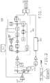
- the direct conversion receiver DCR shown in Fig. 1 includes a clock circuit CLK controlling it and providing timing signals according to the TDMA structure of Fig. 2 which consists of time slots SI arranged in (not shown) frames and multiframes.
- the time slots SI may contain data and/or control information to be received by the direct conversion receiver DCR and/or to be transmitted by a (not shown) transmitter accompanying DCR.
- the type of data (voice, control, ...) and time slot assignment to a station transmitting the data (the transmitter accompanying DCR, a base station or a mobile subscriber transmitting to DCR, ...) are predetermined and are communicated to DCR when a first communication between DCR and e.g. a base station or mobile subscriber is started up.
- the time slots carrying data to be received by the direct conversion receiver DCR each include a leading part LE and a data part DATA as also shown in Fig. 2.
- the purpose of the leading part LE is explained hereinafter.
- the data part DATA contains data sent by a base station or a mobile subscriber to DCR.
- the direct conversion receiver DCR includes an antenna ANT for receiving analog modulating signals which each correspond to a digital signal and are modulated on a carrier with a carrier frequency FC. These signals are so-called Gaussian Minimum Shift Keying (GMSK) modulated signals.
- GMSK Gaussian Minimum Shift Keying
- the antenna ANT is connected to an input of a low noise high frequency amplifier LNA having a gain mode GM, which is set to either of two modes dependent upon the level of the received analog modulating signal modulated carrier.
- a control input of LNA is connected to a clock circuit CLK, and an output of it is connected to a demodulator circuit MIX,LO which constitutes a so-called GMSK-demodulator.
- This demodulator circuit includes a mixer MIX which consists of two coupled so-called correlators CO1 and CO2 and a ⁇ /2 phase shifter PHS connected between CO1 and CO2 and which is connected to a local oscillator LO as shown in Fig. 1.
- Such correlators and such a mixer are e.g. described in the book "Digital Communications - fundamentals and applications" by B. Sklar, published by Prentice-Hall International Editions, 1988, pp. 90 - 91 and 142 - 144, respectively.
- the respective outputs of the correlators CO1 and CO2 are each coupled to a cascaded connection of a lowpass filter, an amplifier and an offset correction circuit, viz. LP1/A1/OCC for CO1 and LP1'/A1'/OCC' for CO2.
- An output of OCC and an output of OCC' are both connected to inputs of a so-called digital signal processor DSP, an output of which is via a digital-to-analog convertor DAC3 coupled to a loudspeaker LS.
- DSP as well as LP1/A1/OCC and LP1'/A1'/OCC' are part of a baseband circuit which is DC-coupled to the demodulator circuit MIX,LO.
- An output of A1 is connected to an input of a comparator circuit SB/LP2/A2, more specifically to a non-inverting first input of a summing stage SB included therein.
- An output of SB is coupled to an input X1 of an analog to digital convertor ADC via the cascaded connection of a low pass filter LP2 and an amplifier stage A2 both included in the comparator circuit.
- X1 is coupled to an inverting second input of SB via the cascaded connection of a comparator COMP and a successive approximative digital to analog convertor DAC2 which is controlled by the clock circuit CLK.
- a non-inverting input of COMP is connected to X1, whereas an inverting input of COMP is connected to a ground terminal GND providing a zero reference voltage.
- An output of ADC is connected to an averaging circuit AV which together with ADC forms a signal averaging circuit, and an output of which is coupled to a non-inverting input of a subtracter circuit SD.
- AV is controlled by a timing signal provided by the clock circuit CLK.
- a small memory SKN storing a reference average value of each of the received analog signals is connected to an inverting input of SD. As the reference average value of each of the analog signals is assumed to be identical, SKN includes only one storage location storing this value.
- An output of the summing stage SD is connected to a first input of a digital filter or calculating means DIGF1 an output of which is connected to a first input of a storage means MEM storing different offset correction values for different carrier frequencies FC and different gain modes GM as will be explained hereinafter.
- MEM is controlled by a control circuit CC.
- An output of MEM is connected to a second input of DIGF1 and is coupled to an inverting third input of the summing stage SB via a digital to analog convertor DAC1.
- the output of SD is furthermore connected to a first input of a second digital filter DIGF2 a second input of which is connected to the output of ADC and an output of which constitutes the output of OCC connected to DSP.
- the direct conversion receiver DCR is synchronized to the TDMA structure, i.e. the timing signals provided by the clock circuit CLK to LNA, DAC2 and AV are synchronized to the TDMA structure for which a synchronization signal transmitted by e.g. a base station and received by DCR is used, and the assigned time slots and the sources, i.e. base station or mobile subscribers, they are assigned to, are known in the DCR as a result of received control information.
- the leading part LE included in such an assigned time slot is provided in order for the direct conversion receiver DCR to be able to adjust to varying power levels of received signals, these levels varying e.g.
- the carrier modulated with an analog modulating signal corresponding to a digital signal is received.
- This analog signal is GMSK modulated on a carrier with a carrier frequency FC.
- the carrier frequency FC on which an analog signal sent by one and the same source, i.e. base station or mobile subscribers, is modulated, changes from time slot to slot according to a pre-agreed pattern, which is known in the art as frequency-hopping. This technique is described e.g. in the above book by B. Sklar, pp. 555 - 562.
- the pre-agreed pattern according to which the carrier frequency changes is e.g. communicated to the direct conversion receiver DCR when a communication between one of the base stations or mobile subscribers and DCR is started up, and is then known in the control circuit CC.
- the analog modulating signal modulated carrier is received via the antenna ANT and amplified by the low noise amplifier LNA the gain mode GM of which is set to one of two possible modes depending on the level of the received modulated carrier, and is also known in CC.
- the modulated carrier is then demodulated by the mixer MIX by multiplying it with a local oscillator signal which is provided by LO and which has the same frequency as the carrier wave.
- LO local oscillator signal
- two demodulated analog signal parts are obtained, one corresponding to a so-called in-phase (I) channel of the analog modulating signal which is output by CO1, and another corresponding to a so-called quadrature (Q) channel of the analog modulating signal which is output by CO2.
- Both the I- and Q-channels are baseband signals, i.e.
- the I- and Q-channels are then filtered in the lowpass filters LP1 and LP1' and amplified by A1 and A1', respectively. Both channels henceforth being processed in the same way by OCC and OCC', respectively, only the processing of one of the two channels, viz. the I-channel, is discussed hereafter.
- the I-channel present at the output of A1 corresponds to a digital signal part consisting of bits which after coding and pulse shaping constitute the I-channel.
- the average value of the analog signal depends on the coding technique used and possibly also on the pulse shaping waveform applied.
- AMI-coding is applied one can easily show that the average value of the analog signal is zero.
- a coding technique giving rise to a zero average value is used.
- the I-channel constituting an input signal for OCC, is applied to the non-inverting input of the summing stage SB wherein a variable parameter offset correction value and a single offset correction value both discussed hereinafter are subtracted from it.
- the variable parameter offset correction value is provided by the storage means MEM after being converted to an analog value by DAC1.
- the result of the subtraction is filtered in the lowpass filter LP2 and then amplified by the amplifier stage A2 so providing a difference signal at input X1 of ADC.
- a first source of offset is due to the signal provided by the local oscillator LO and appearing at the local oscillator input of the mixer MIX, i.e. at the local oscillator inputs of both CO1 and CO2, partly leaking to the input of the mixer MIX to which the received modulated carrier is applied, due to capacitive or inductive crosstalk between the latter two inputs.
- this leaked local oscillator signal part is added to the received modulated carrier.
- a first offset part is generated due to the mixer MIX multiplying the thus changed received signal with the local oscillator signal.
- the result thereof includes the square of the local oscillator signal and ergo, since the local oscillator signal is assumed to be sinusoidal, a DC part constituting the first offset part.
- this first offset part varies with the frequency of the local oscillator signal.
- a second source of offset is due to so-called self-mixing, i.e. the received modulated carrier applied to the received signal input of MIX partly leaks to the local oscillator input of the mixer MIX.
- the result of the multiplication operation performed by the mixer includes a DC part resulting from the square of the received signal, an offset is generated which depends on the frequency of the received signal and on its power level.
- the frequency dependency is due to the coupling between the local oscillator and the high frequency part.
- dem represents the demodulated analog signal
- losi represents the signal provided by the local oscillator which is sinusoidal with amplitude A
- rec represents the received modulated carrier which, although occupying a non-zero bandwidth, is assumed substantially sinusoidal and is therefore also represented as a sinusoid with amplitude B
- ⁇ represents the fraction of the local oscillator signal leaking to the received signal input of MIX
- ⁇ represents the fraction of the received signal leaking to the local oscillator input of MIX.
- a third offset source is caused by so-called front-end pick-up, which is due to the local oscillator signal partly leaking via the environment of the receiver, e.g. via a housing surrounding it, to the input of the low noise amplifier LNA and to the antenna ANT where this leaked local oscillator signal part is added to the received signal.
- the first offset source this causes an offset to be generated by the mixer which is also dependent upon the frequency of the local oscillator signal.
- the main difference however with the first offset source, and also the reason for distinguishing between the first and the third offset source is that since this offset is due to leakage via the environment it is also influenced by the position of the direct conversion receiver DCR and thus e.g. by a person holding the receiver or a handset thereof and by the position of this handset.
- the second and the third mentioned offset source provide unpredictable offset parts, the second due to its dependency upon the power level and the frequency of the received signals and the third due to its position dependency, whereas the offset introduced by the first mentioned offset source could theoretically be measured and compensated for at fabrication since it only depends on the frequency - and the power level - of the local oscillator signal which is known. However due to alteration of component characteristics with time such compensation would not remain accurate. The same applies to offset introduced due to component mismatches which, since it is quasi-constant, is also referred to as static offset. To be noted here that even received signals not to be demodulated and thus filtered out in the lowpass filters LP1 and LP1' introduce offset, as these signals too leak to the local oscillator input of MIX.
- the combination of the offset sources mentioned above provides an offset which depends upon the power level and the frequency of the local oscillator signal as well as the received signals, and the position of the receiver.
- the offset mentioned is due to leakage because of capacitive or inductive coupling in the direct conversion receiver, it is composed of a portion due to leakage to the input of LNA and a portion due to leakage to the output of LNA.
- the first portion being influenced by the gain mode GM unlike the second portion, the offset at different values of the gain mode GM is different and dependent upon the ratio of the first portion to the second portion.
- the carrier frequency FC and the gain mode GM constitute variable parameters on which the offset depends. This offset is compensated in the following way.
- the clock circuit CLK provides a signal switching off the LNA and thereby inhibiting the received modulated carrier to reach the mixer MIX. Consequently, during LE only offset due to the above mentioned first offset source and static offset is added to the demodulated analog signal which however is zero since no received modulated carrier is applied during LE.
- the signal applied to the non-inverting input of the summing stage SB only consists of offset.
- the output of SB, filtered by LP2 and amplified by A2 is applied to the non-inverting input of COMP which compares it to the expected value of the signal at X1 during LE when no offset would be generated, i.e. zero provided by GND.
- COMP When the signal at X1 is positive, COMP provides a positive voltage at its output indicating a binary 1, whereas when the signal at X1 is negative a negative voltage is provided indicating a binary 0.
- COMP acts as a one bit analog to digital convertor.
- the thus obtained digital output signal of COMP controls the successive approximative digital to analog convertor DAC2 which, within the leading part LE and in successive steps, generates a single offset correction value to be applied to the inverting second input of SB by successively adjusting a digital number to a value which converted to an analog signal provides the single offset correction value making the signal at X1 closer to zero at each step.
- the digital output signal of COMP is first monitored by DAC2 and then a next bit of the digital number is either set to 1 or to 0 dependent upon the signal of COMP representing a binary 1 or 0, respectively, thereby increasing the accuracy of the single offset correction value by one bit.
- COMP provides a binary 1 at its output which causes a bit of the digital number generated by DAC2 to be set to 1 thus increasing its analog output signal and providing a larger single offset correction value to be subtracted in SB and thus decreasing the signal at X1.
- the accuracy of the offset compensation depends on the accuracy of DAC2.
- the DCR adjusts to varying power levels of received signals as mentioned above.
- DAC2 since the implementation of DAC2 is not a subject of the invention, it is not described here. Furthermore, other possibilities for determining this single offset correction value can be thought of. Knowing the average value of the analog baseband signal is zero one could e.g. measure the average value of the analog baseband signal over a number of time slots, the result of which then provides the single offset correction value. In order to avoid distortion of the measured average value by high signal power levels, one could e.g. only use time slots in the calculation in which signals with a power level below a predetermined limit are received.
- a second more accurate offset correction value is determined as follows at each of the assigned time slots.
- the signal at X1 is converted by ADC to a digital value at the rate of the bits of the digital signal corresponding to the demodulated analog signal thereby providing consecutive digital values indicating the power level of each bit of the difference signal at X1.
- These digital values are then applied to the averaging circuit AV which can easily be implemented as a small digital processor.
- AV calculates an instant average value of the digital values over the data part DATA of an assigned time slot, the boundaries of this data part being indicated by the signal applied to AV by the clock circuit CLK.
- the thus calculated instant average value is then applied to the non-inverting input of the subtracter circuit SD where the reference average value, here zero, of the analog baseband signal is subtracted from it.
- the result thereof constitutes a resulting control value which is applied to the digital filter DIGF1.
- Another input signal for DIGF1 is supplied by the storage means MEM and constitutes a variable parameter offset correction value as calculated previously for the values of the variable parameters, i.e. gain mode GM and carrier frequency FC, associated to the present assigned time slot.
- This variable parameter offset correction value which is the one subtracted from the demodulated analog signal in SB as mentioned above, is read from the storage location of MEM indicated by the signal at the control input of MEM and provided by the control circuit CC which is derived from the current carrier frequency FC and gain mode GM.
- a new variable parameter offset correction value is calculated from the output signal of SD and the value provided by MEM as seen in equations (2a) and (2b) which constitutes the so-called z-transform of equation (2a) as indicated by Z , and where ⁇ is a proportionality factor, meas indicates the output value of SD, memv indicates the value provided by MEM and memvn indicates the newly calculated variable parameter offset correction value.
- ⁇ is a proportionality factor
- meas indicates the output value of SD
- memv indicates the value provided by MEM
- memvn indicates the newly calculated variable parameter offset correction value.
- the storage means MEM is initialized with estimated values of the variable parameter offset correction values when the direct conversion receiver DCR is started up, and hence, that these estimated values constitute the first of the above mentioned previously calculated variable parameter offset correction values.
- a bad estimate merely causes the stored values to somewhat longer provide a bad offset correction so that the single offset correction value may be needed somewhat longer.
- the estimate of the average value can be improved by calculating it over a large number of time slots, thus decreasing the standard deviation by a factor equal to the square root of this number of time slots. Since the average is to be calculated only over time slots with the same carrier frequency FC and the same gain mode GM, the number of time slots needed to obtain an accurate estimate of the average value and thereby of the introduced offset is especially large when a large number of different carrier frequencies and gain modes is used.
- the offset on the signal at the output of SB may during this time be relatively large so that the amplifier A2 is possibly saturated.
- the earlier described single offset correction value is calculated and applied to keep the offset still present at the output of SB within boundaries.
- the analog demodulated signal provided by the demodulator circuit O represents the difference signal as present after ADC, A the amplification of the cascaded connection of LP2, A2 and ADC, O ' represents the output signal of the digital filter DIGF2, and E(x) represents the average value of x over the data part DATA of a time slot.
- the variable parameter offset correction value as well as the resulting control value are both represented by the average value E(O) of the difference signal which can only be exact if ADC and DAC1 would provide a perfect conversion and if the offset would not change in function of time.
- the single offset correction value not changing over the data part DATA of a time slot, it is not explicitly mentioned in this equation but is already incorporated in I .
- the average value E(O) of O is substantially equal to the average value E(I) of I , i.e. the offset on O is substantially equal to that on I and is hence relatively decreased by a factor A .
- the average value E(O') of O' is zero as indicated by equation (3) and hence offset correction is again improved.
- the final offset corrected signal O ' can e.g. also be obtained by subtracting from O an instant average value calculated over subsequent time slots without taking the variation of the offset with FC or GM into account. This provides a less accurate offset compensation which may nevertheless be sufficient.
Priority Applications (3)
| Application Number | Priority Date | Filing Date | Title |
|---|---|---|---|
| DE69228816T DE69228816T2 (de) | 1992-10-28 | 1992-10-28 | Offsetgleichspannungskorrektur für Direktmisch-TDMA-Empfänger |
| EP92203303A EP0594894B1 (fr) | 1992-10-28 | 1992-10-28 | Correction du décalage de la tension continue pour récepteur AMRT à conversion directe |
| US08/144,276 US5422889A (en) | 1992-10-28 | 1993-10-28 | Offset correction circuit |
Applications Claiming Priority (1)
| Application Number | Priority Date | Filing Date | Title |
|---|---|---|---|
| EP92203303A EP0594894B1 (fr) | 1992-10-28 | 1992-10-28 | Correction du décalage de la tension continue pour récepteur AMRT à conversion directe |
Publications (2)
| Publication Number | Publication Date |
|---|---|
| EP0594894A1 true EP0594894A1 (fr) | 1994-05-04 |
| EP0594894B1 EP0594894B1 (fr) | 1999-03-31 |
Family
ID=8210999
Family Applications (1)
| Application Number | Title | Priority Date | Filing Date |
|---|---|---|---|
| EP92203303A Expired - Lifetime EP0594894B1 (fr) | 1992-10-28 | 1992-10-28 | Correction du décalage de la tension continue pour récepteur AMRT à conversion directe |
Country Status (3)
| Country | Link |
|---|---|
| US (1) | US5422889A (fr) |
| EP (1) | EP0594894B1 (fr) |
| DE (1) | DE69228816T2 (fr) |
Cited By (30)
| Publication number | Priority date | Publication date | Assignee | Title |
|---|---|---|---|---|
| WO1996028885A1 (fr) * | 1995-03-09 | 1996-09-19 | Ericsson Inc. | Compensation de la pente, de la derive et du decalage dans les recepteurs a frequence intermediaire nulle |
| WO1997023032A1 (fr) * | 1995-12-15 | 1997-06-26 | Telefonaktiebolaget Lm Ericsson (Publ) | Etalonnage numerique d'un emetteur-recepteur |
| WO1997029551A1 (fr) * | 1996-02-08 | 1997-08-14 | Nokia Mobile Phones Ltd. | Procede et configuration de circuits permettant d'attenuer la tension de decalage d'un signal |
| EP0840484A2 (fr) * | 1996-10-31 | 1998-05-06 | Nec Corporation | Correction de décalage continu dans systèmes AMRT |
| WO1998032221A1 (fr) * | 1997-01-17 | 1998-07-23 | Ericsson Inc. | Procede et dispositif pour compenser les desequilibres entre signaux en quadrature |
| EP0865165A2 (fr) * | 1997-03-14 | 1998-09-16 | Kabushiki Kaisha Toshiba | Appareil radio |
| WO1998042071A1 (fr) * | 1997-03-18 | 1998-09-24 | Telefonaktiebolaget Lm Ericsson | Recepteur radio |
| US5896562A (en) * | 1996-04-01 | 1999-04-20 | Nokia Mobile Phones, Ltd. | Transmitter/receiver for transmitting and receiving of an RF signal in two frequency bands |
| US6009126A (en) * | 1996-09-06 | 1999-12-28 | U.S. Philips Corporation | Zero-IF receiver |
| WO2000033458A1 (fr) * | 1998-11-30 | 2000-06-08 | Conexant Systems, Inc. | Recepteur pour signaux rf |
| WO2000046914A1 (fr) * | 1999-02-03 | 2000-08-10 | Infineon Technologies Ag | Procede et circuit pour commander la compensation de tensions de decalage d'un circuit de reception radio integre dans un module de circuit |
| GB2346777A (en) * | 1999-02-12 | 2000-08-16 | Nokia Mobile Phones Ltd | DC offset correction in a direct conversion receiver |
| US6115593A (en) * | 1996-05-07 | 2000-09-05 | Nokia Mobile Phones, Ltd. | Elimination of D.C. offset and spurious AM suppression in a direct conversion receiver |
| WO2001005025A1 (fr) * | 1999-07-07 | 2001-01-18 | Siemens Aktiengesellschaft | Procede et dispositif pour corriger une alteration de signal utile |
| US6324389B1 (en) | 1996-02-08 | 2001-11-27 | Nokia Mobile Phones Ltd. | Method and circuit arrangement for processing a received signal |
| WO2002056484A2 (fr) * | 2001-01-09 | 2002-07-18 | Telefonaktiebolaget L M Ericsson (Publ) | Recepteur radio |
| DE10128236A1 (de) * | 2001-06-11 | 2002-08-01 | Infineon Technologies Ag | Verfahren zur Kompensation einer stufenförmigen DC-Störung in einem digitalen Basisbandsignal eines Homodyn-Funkempfängers |
| EP1391997A2 (fr) * | 1994-12-28 | 2004-02-25 | Telefonaktiebolaget Lm Ericsson | Récepteur à conversion directe et à compensation numérique |
| US6707860B1 (en) | 1999-02-05 | 2004-03-16 | Alcatel | DC offset correction for direct-conversion receiver |
| US6714765B1 (en) | 1999-06-10 | 2004-03-30 | Nokia Mobile Phones Ltd. | Transceiver for transmitting and receiving an RF signal on at least two frequency ranges |
| US6941121B2 (en) * | 2001-05-18 | 2005-09-06 | Rf Micro Devices, Inc. | Method for calibrating a DC offset cancellation level for direct conversion receivers |
| US6947495B2 (en) | 2000-10-30 | 2005-09-20 | Texas Instruments Incorporated | Method for estimating and removing a time-varying DC-offset |
| WO2005101671A3 (fr) * | 2004-04-13 | 2006-01-12 | Maxlinear Inc | Procede et appareil pour supprimer le glissement de frequence de double conversion |
| EP1632039A1 (fr) * | 2003-06-06 | 2006-03-08 | Interdigital Technology Corporation | Recepteur bande de base numerique avec circuits de commande de gain et de decharge cc |
| GB2424326A (en) * | 2005-03-18 | 2006-09-20 | Motorola Inc | Direct conversion FM receiver employing average DC offset correction |
| CN102123116A (zh) * | 2011-03-11 | 2011-07-13 | 京信通信系统(中国)有限公司 | 一种直流偏置校准方法及其装置 |
| US8285240B2 (en) | 2004-12-10 | 2012-10-09 | Maxlinear, Inc. | Harmonic reject receiver architecture and mixer |
| US8306157B2 (en) | 2004-10-12 | 2012-11-06 | Maxlinear, Inc. | Receiver architecture with digitally generated intermediate frequency |
| US8311156B2 (en) | 2004-10-12 | 2012-11-13 | Maxlinear, Inc. | Hybrid receiver architecture using upconversion followed by direct downconversion |
| US8396173B2 (en) | 2007-10-01 | 2013-03-12 | Maxlinear, Inc. | I/Q calibration techniques |
Families Citing this family (70)
| Publication number | Priority date | Publication date | Assignee | Title |
|---|---|---|---|---|
| US5609688A (en) * | 1993-05-07 | 1997-03-11 | Fujitsu Ltd. | Apparatus for producing semiconductor device |
| US5584059A (en) * | 1993-06-30 | 1996-12-10 | Motorola, Inc. | DC offset reduction in a zero-if transmitter |
| DE4341937A1 (de) * | 1993-12-09 | 1995-06-14 | Philips Patentverwaltung | Elektrisches Gerät mit einer Anordnung zur Kompensation eines Gleichspannungsanteils |
| JPH07250115A (ja) * | 1994-03-09 | 1995-09-26 | Toshiba Corp | デジタルデータ受信装置 |
| US5734966A (en) * | 1995-01-20 | 1998-03-31 | Diablo Research Corporation | Wireless communication system for adapting to frequency drift |
| GB9617423D0 (en) * | 1995-10-11 | 1996-10-02 | Philips Electronics Nv | Receiver circuit |
| US5659372A (en) * | 1995-12-22 | 1997-08-19 | Samsung Electronics Co., Ltd. | Digital TV detector responding to final-IF signal with vestigial sideband below full sideband in frequency |
| US5838735A (en) * | 1996-07-08 | 1998-11-17 | Telefonaktiebolaget Lm Ericsson | Method and apparatus for compensating for a varying d.c. offset in a sampled signal |
| US5818872A (en) * | 1996-12-31 | 1998-10-06 | Cirrus Logic, Inc. | Timing offset error extraction method and apparatus |
| DE69818327T2 (de) * | 1997-03-05 | 2004-07-01 | Nec Corp. | Direktmischempfänger zur Unterdrückung von Offset-Gleichspannungen |
| US5881096A (en) * | 1997-06-05 | 1999-03-09 | Itt Manufacturing Enterprises, Inc. | Method for removing bias in a frequency hopping digital communication system |
| US6006079A (en) * | 1997-06-13 | 1999-12-21 | Motorola, Inc. | Radio having a fast adapting direct conversion receiver |
| US6240100B1 (en) * | 1997-07-31 | 2001-05-29 | Motorola, Inc. | Cellular TDMA base station receiver with dynamic DC offset correction |
| US7065327B1 (en) | 1998-09-10 | 2006-06-20 | Intel Corporation | Single-chip CMOS direct-conversion transceiver |
| SE512965C2 (sv) * | 1998-09-15 | 2000-06-12 | Ericsson Telefon Ab L M | Metod och anordning för att reducera fel i DC nivå i ett TDMA system |
| US6298096B1 (en) | 1998-11-19 | 2001-10-02 | Titan Corporation | Method and apparatus for determination of predistortion parameters for a quadrature modulator |
| US6757340B1 (en) * | 1999-02-22 | 2004-06-29 | Telefonaktiebolaget L M Ericsson (Publ) | Radio receiver and method for preloading an average DC-offset into a channel filter |
| US6584090B1 (en) * | 1999-04-23 | 2003-06-24 | Skyworks Solutions, Inc. | System and process for shared functional block CDMA and GSM communication transceivers |
| JP2000349840A (ja) * | 1999-06-03 | 2000-12-15 | Matsushita Electric Ind Co Ltd | ベースバンド信号オフセット補正回路及び方法、この補正回路を備えたfsk受信装置 |
| US6535560B1 (en) | 1999-06-03 | 2003-03-18 | Ditrans Corporation | Coherent adaptive calibration system and method |
| US6826390B1 (en) * | 1999-07-14 | 2004-11-30 | Fujitsu Limited | Receiver, transceiver circuit, signal transmission method, and signal transmission system |
| CA2281236C (fr) * | 1999-09-01 | 2010-02-09 | Tajinder Manku | Methodes rf de conversion directe au moyen d'un signal virtuel d'oscillateur local |
| MY133723A (en) * | 1999-09-17 | 2007-11-30 | Ericsson Telefon Ab L M | "apparatus and method for substantially eliminating a near-channel interfering amplitude modulated signal" |
| US6188282B1 (en) | 1999-10-08 | 2001-02-13 | Ericsson Inc. | Differential amplifier with reduced even order non-linearity and associated methods |
| US6823174B1 (en) | 1999-10-11 | 2004-11-23 | Ditrans Ip, Inc. | Digital modular adaptive antenna and method |
| US20050088338A1 (en) * | 1999-10-11 | 2005-04-28 | Masenten Wesley K. | Digital modular adaptive antenna and method |
| GB2382331B (en) * | 1999-11-02 | 2003-10-01 | Allan William Stobart | Improvements in and relating to road and rail tankers |
| US6704349B1 (en) * | 2000-01-18 | 2004-03-09 | Ditrans Corporation | Method and apparatus for canceling a transmit signal spectrum in a receiver bandwidth |
| US6259752B1 (en) * | 2000-02-01 | 2001-07-10 | Conexant Systems, Inc. | System for cancelling internal interference in a receiver |
| US6771945B1 (en) * | 2000-05-24 | 2004-08-03 | General Dynamics Decision Systems, Inc. | Dynamic DC balancing of a direct conversion receiver and method |
| US6868128B1 (en) * | 2000-07-05 | 2005-03-15 | Rfmd Wpan, Inc. | Method and apparatus for calibrating DC-offsets in a direct conversion receiver |
| ATE313166T1 (de) | 2000-10-30 | 2005-12-15 | Texas Instruments Inc | Vorrichtung zum ausgleichen des dc-offsets eines quadratur-demodulators , und verfahren dazu |
| CN1214585C (zh) * | 2000-11-23 | 2005-08-10 | 皇家菲利浦电子有限公司 | 具有直流控制环路及直流阻断电路的直流偏移校正电路 |
| US7076225B2 (en) * | 2001-02-16 | 2006-07-11 | Qualcomm Incorporated | Variable gain selection in direct conversion receiver |
| US6873832B2 (en) * | 2001-09-28 | 2005-03-29 | Broadcom Corporation | Timing based LNA gain adjustment in an RF receiver to compensate for intermodulation interference |
| JP2003198404A (ja) * | 2001-12-26 | 2003-07-11 | Matsushita Electric Ind Co Ltd | ダイレクトコンバージョン受信機及びこれを用いた移動無線機、並びにrf信号の受信方法 |
| US6816718B2 (en) * | 2002-02-07 | 2004-11-09 | Rf Micro Devices, Inc. | DC offset correction using dummy amplifier |
| US6862439B2 (en) * | 2002-06-28 | 2005-03-01 | Nokia Corporation | Offset compensation in a direct-conversion receiver |
| US7536165B2 (en) | 2002-07-24 | 2009-05-19 | Nxp B.V. | Offset correction for down-conversion mixers |
| US7146146B2 (en) * | 2003-01-31 | 2006-12-05 | Ditrans Ip, Inc. | Systems and methods for coherent adaptive calibration in a receiver |
| US7190931B2 (en) * | 2003-09-29 | 2007-03-13 | Intel Corporation | Receiver calibration apparatus, method, and system |
| US7265694B2 (en) * | 2004-03-25 | 2007-09-04 | Texas Instruments Incorporated | System and method for successive approximation |
| US7336937B2 (en) | 2004-05-05 | 2008-02-26 | Nokia Corporation | Compensation of a DC offset in a receiver |
| EP1792410B1 (fr) * | 2004-09-06 | 2009-02-11 | Freescale Semiconductors, Inc. | Dispositif de communications sans fil et interface de donnees |
| US7313376B1 (en) * | 2004-11-12 | 2007-12-25 | Rf Micro Devices, Inc. | DC offset correction for a wireless communication system |
| US6992611B1 (en) | 2005-02-25 | 2006-01-31 | Analog Devices, Inc. | DC-coupled wideband signal converters |
| US20070025417A1 (en) * | 2005-07-28 | 2007-02-01 | Freescale Semiconductor Inc. | System and method for mitigating filter transients in an ultra wideband receiver |
| WO2007057844A1 (fr) * | 2005-11-18 | 2007-05-24 | Koninklijke Philips Electronics N.V. | Estimation de decalage cc |
| US7903761B2 (en) * | 2006-03-31 | 2011-03-08 | Qualcomm Incorporated | UWB radio interface with DC offset |
| US7933361B2 (en) * | 2006-04-05 | 2011-04-26 | Integrated System Solution Corp. | Hybrid DC-offset reduction method and system for direct conversion receiver |
| KR100782326B1 (ko) * | 2006-05-06 | 2007-12-06 | 삼성전자주식회사 | 직접 변환 수신기의 베이스 밴드용 아날로그 집적회로 및dc 오프셋 제거 방법 |
| US7778252B2 (en) * | 2006-05-18 | 2010-08-17 | Freescale Semiconductor, Inc. | Hardware monitor of LIN time budget |
| US9576046B2 (en) | 2011-11-16 | 2017-02-21 | Ptc Inc. | Methods for integrating semantic search, query, and analysis across heterogeneous data types and devices thereof |
| US8909641B2 (en) | 2011-11-16 | 2014-12-09 | Ptc Inc. | Method for analyzing time series activity streams and devices thereof |
| US9098312B2 (en) | 2011-11-16 | 2015-08-04 | Ptc Inc. | Methods for dynamically generating an application interface for a modeled entity and devices thereof |
| WO2014145084A1 (fr) | 2013-03-15 | 2014-09-18 | Ptc Inc. | Procédés de gestion d'applications à l'aide d'une modélisation et d'un étiquetage sémantiques, et dispositifs associés |
| CN103401529B (zh) * | 2013-06-25 | 2017-05-17 | 杨俊杰 | 复数带通滤波器电路的直流偏差校正方法 |
| CN103326735B (zh) * | 2013-06-25 | 2017-03-15 | 杨俊杰 | 一种无线中频接收电路系统的直流偏差校正方法 |
| US10025942B2 (en) | 2014-03-21 | 2018-07-17 | Ptc Inc. | System and method of establishing permission for multi-tenancy storage using organization matrices |
| US9467533B2 (en) | 2014-03-21 | 2016-10-11 | Ptc Inc. | System and method for developing real-time web-service objects |
| US9350812B2 (en) | 2014-03-21 | 2016-05-24 | Ptc Inc. | System and method of message routing using name-based identifier in a distributed computing environment |
| US9462085B2 (en) | 2014-03-21 | 2016-10-04 | Ptc Inc. | Chunk-based communication of binary dynamic rest messages |
| US9560170B2 (en) | 2014-03-21 | 2017-01-31 | Ptc Inc. | System and method of abstracting communication protocol using self-describing messages |
| US10313410B2 (en) | 2014-03-21 | 2019-06-04 | Ptc Inc. | Systems and methods using binary dynamic rest messages |
| US9350791B2 (en) | 2014-03-21 | 2016-05-24 | Ptc Inc. | System and method of injecting states into message routing in a distributed computing environment |
| US9961058B2 (en) | 2014-03-21 | 2018-05-01 | Ptc Inc. | System and method of message routing via connection servers in a distributed computing environment |
| US9762637B2 (en) | 2014-03-21 | 2017-09-12 | Ptc Inc. | System and method of using binary dynamic rest messages |
| WO2015143416A1 (fr) | 2014-03-21 | 2015-09-24 | Ptc Inc. | Systèmes et procédés permettant de développer et d'utiliser des applications de données en temps réel |
| WO2016142424A1 (fr) * | 2015-03-09 | 2016-09-15 | Sony Corporation | Dispositif et procédé pour couler un composant |
| EP3300435B1 (fr) * | 2016-09-27 | 2020-04-08 | Intel IP Corporation | Dispositif de communication et procede de reprise de reception de donnees |
Citations (4)
| Publication number | Priority date | Publication date | Assignee | Title |
|---|---|---|---|---|
| US4878029A (en) * | 1988-12-05 | 1989-10-31 | General Electric Company | Complex digital sampling converter for demodulator |
| WO1991014311A1 (fr) * | 1990-03-07 | 1991-09-19 | At&E Corporation | Recepteur radio a fi nulle pour fonctionnement intermittent |
| EP0474615A2 (fr) * | 1990-09-06 | 1992-03-11 | Telefonaktiebolaget L M Ericsson | Procédé de l'élimination de la tension continue de décalage pour un radio-récepteur |
| US5144256A (en) * | 1990-12-31 | 1992-09-01 | Samsung Electronics Co., Ltd. | Method and apparatus for demodulating a GMSK signal |
Family Cites Families (4)
| Publication number | Priority date | Publication date | Assignee | Title |
|---|---|---|---|---|
| EP0232181B1 (fr) * | 1986-02-07 | 1992-09-16 | Matsushita Electric Industrial Co., Ltd. | Appareil de reproduction d'informations numériques |
| DE3932247A1 (de) * | 1989-09-27 | 1991-04-04 | Biotechnolog Forschung Gmbh | Elektrodenmaterial, elektroden, verfahren zur herstellung und verwendung der elektrode |
| US5263196A (en) * | 1990-11-19 | 1993-11-16 | Motorola, Inc. | Method and apparatus for compensation of imbalance in zero-if downconverters |
| US5307379A (en) * | 1992-04-27 | 1994-04-26 | Motorola, Inc. | Automatic noise characterization for optimally enabling a receiver |
-
1992
- 1992-10-28 EP EP92203303A patent/EP0594894B1/fr not_active Expired - Lifetime
- 1992-10-28 DE DE69228816T patent/DE69228816T2/de not_active Expired - Lifetime
-
1993
- 1993-10-28 US US08/144,276 patent/US5422889A/en not_active Expired - Lifetime
Patent Citations (4)
| Publication number | Priority date | Publication date | Assignee | Title |
|---|---|---|---|---|
| US4878029A (en) * | 1988-12-05 | 1989-10-31 | General Electric Company | Complex digital sampling converter for demodulator |
| WO1991014311A1 (fr) * | 1990-03-07 | 1991-09-19 | At&E Corporation | Recepteur radio a fi nulle pour fonctionnement intermittent |
| EP0474615A2 (fr) * | 1990-09-06 | 1992-03-11 | Telefonaktiebolaget L M Ericsson | Procédé de l'élimination de la tension continue de décalage pour un radio-récepteur |
| US5144256A (en) * | 1990-12-31 | 1992-09-01 | Samsung Electronics Co., Ltd. | Method and apparatus for demodulating a GMSK signal |
Non-Patent Citations (1)
| Title |
|---|
| 5th International Conference on Radio Receivers and Associated Systems, 23 27 July 1990, Cambridge, GB; IEE, London, GB, 1990; Bollinger and Vollenweider: "Some experiments on direct - conversion receivers" * |
Cited By (64)
| Publication number | Priority date | Publication date | Assignee | Title |
|---|---|---|---|---|
| EP1391997A3 (fr) * | 1994-12-28 | 2004-06-02 | Telefonaktiebolaget LM Ericsson (publ) | Récepteur à conversion directe et à compensation numérique |
| EP1391997A2 (fr) * | 1994-12-28 | 2004-02-25 | Telefonaktiebolaget Lm Ericsson | Récepteur à conversion directe et à compensation numérique |
| US5712637A (en) * | 1995-03-09 | 1998-01-27 | Ericsson Inc. | Slope, drift and offset compensation in zero-IF receivers |
| WO1996028885A1 (fr) * | 1995-03-09 | 1996-09-19 | Ericsson Inc. | Compensation de la pente, de la derive et du decalage dans les recepteurs a frequence intermediaire nulle |
| US6473471B2 (en) | 1995-03-09 | 2002-10-29 | Ericsson Inc | Slope drift and offset compensation in zero-if receivers |
| EP0952665A3 (fr) * | 1995-03-09 | 2002-07-10 | Ericsson Inc. | Compensation de la pente, de la dérive et du décalage dans les récepteurs à fréquence intermédiaire nulle |
| AU709812B2 (en) * | 1995-03-09 | 1999-09-09 | Ericsson Inc. | Slope, drift and offset compensation in zero-IF receivers |
| EP0952665A2 (fr) * | 1995-03-09 | 1999-10-27 | Ericsson Inc. | Compensation de la pente, de la dérive et du décalage dans les récepteurs à fréquence intermédiaire nulle |
| WO1997023032A1 (fr) * | 1995-12-15 | 1997-06-26 | Telefonaktiebolaget Lm Ericsson (Publ) | Etalonnage numerique d'un emetteur-recepteur |
| KR100450859B1 (ko) * | 1995-12-15 | 2004-11-16 | 텔레폰아크티에볼라게트 엘엠 에릭슨 | 송수신기의디지털교정 |
| CN1080025C (zh) * | 1995-12-15 | 2002-02-27 | 艾利森电话股份有限公司 | 收发信机的数字校准 |
| AU713270B2 (en) * | 1995-12-15 | 1999-11-25 | Telefonaktiebolaget Lm Ericsson (Publ) | Digital calibration of a transceiver |
| US6144243A (en) * | 1996-02-08 | 2000-11-07 | Nokia Mobile Phones Ltd. | Method and circuit arrangement for reducing offset voltage of a signal |
| WO1997029551A1 (fr) * | 1996-02-08 | 1997-08-14 | Nokia Mobile Phones Ltd. | Procede et configuration de circuits permettant d'attenuer la tension de decalage d'un signal |
| US6324389B1 (en) | 1996-02-08 | 2001-11-27 | Nokia Mobile Phones Ltd. | Method and circuit arrangement for processing a received signal |
| US5896562A (en) * | 1996-04-01 | 1999-04-20 | Nokia Mobile Phones, Ltd. | Transmitter/receiver for transmitting and receiving of an RF signal in two frequency bands |
| EP1737137A1 (fr) | 1996-04-01 | 2006-12-27 | Nokia Corporation | Emetteur-récepteur fonctionnant pour deux gammes de fréquence |
| US6115593A (en) * | 1996-05-07 | 2000-09-05 | Nokia Mobile Phones, Ltd. | Elimination of D.C. offset and spurious AM suppression in a direct conversion receiver |
| EP0806841B1 (fr) * | 1996-05-07 | 2006-03-01 | Nokia Corporation | Elimination de DC-offset et suppression des signaux parasitaires AM dans un récepteur à conversion directe |
| EP0865686B1 (fr) * | 1996-09-06 | 2004-12-08 | Koninklijke Philips Electronics N.V. | Recepteur a frequence intermediaire nulle |
| US6009126A (en) * | 1996-09-06 | 1999-12-28 | U.S. Philips Corporation | Zero-IF receiver |
| EP0840484A2 (fr) * | 1996-10-31 | 1998-05-06 | Nec Corporation | Correction de décalage continu dans systèmes AMRT |
| EP0840484A3 (fr) * | 1996-10-31 | 2001-02-21 | Nec Corporation | Correction de décalage continu dans systèmes AMRT |
| US6009317A (en) * | 1997-01-17 | 1999-12-28 | Ericsson Inc. | Method and apparatus for compensating for imbalances between quadrature signals |
| WO1998032221A1 (fr) * | 1997-01-17 | 1998-07-23 | Ericsson Inc. | Procede et dispositif pour compenser les desequilibres entre signaux en quadrature |
| EP1635467A3 (fr) * | 1997-03-14 | 2006-05-24 | Kabushiki Kaisha Toshiba | Appareil radio |
| EP1635467A2 (fr) * | 1997-03-14 | 2006-03-15 | Kabushiki Kaisha Toshiba | Appareil radio |
| EP0865165A2 (fr) * | 1997-03-14 | 1998-09-16 | Kabushiki Kaisha Toshiba | Appareil radio |
| EP0865165A3 (fr) * | 1997-03-14 | 2003-04-02 | Kabushiki Kaisha Toshiba | Appareil radio |
| US7184738B2 (en) | 1997-03-14 | 2007-02-27 | Kabushiki Kaisha Toshiba | Radio apparatus |
| US7590400B2 (en) | 1997-03-14 | 2009-09-15 | Kabushiki Kaisha Toshiba | Radio apparatus |
| US6816712B2 (en) | 1997-03-14 | 2004-11-09 | Kabushiki Kaisha Toshiba | Radio apparatus |
| WO1998042071A1 (fr) * | 1997-03-18 | 1998-09-24 | Telefonaktiebolaget Lm Ericsson | Recepteur radio |
| US6449321B1 (en) | 1997-03-18 | 2002-09-10 | Telefonaktiebolaget Lm Ericsson (Publ) | Radio receiver |
| US6298226B1 (en) | 1998-11-30 | 2001-10-02 | Conexant Systems, Inc. | Receiver for RF signals |
| WO2000033458A1 (fr) * | 1998-11-30 | 2000-06-08 | Conexant Systems, Inc. | Recepteur pour signaux rf |
| US6658244B2 (en) | 1999-02-03 | 2003-12-02 | Infineon Technologies Ag | Method and circuit for compensation control of offset voltages in a radio receiving circuit integrated in a circuit module |
| WO2000046914A1 (fr) * | 1999-02-03 | 2000-08-10 | Infineon Technologies Ag | Procede et circuit pour commander la compensation de tensions de decalage d'un circuit de reception radio integre dans un module de circuit |
| US6707860B1 (en) | 1999-02-05 | 2004-03-16 | Alcatel | DC offset correction for direct-conversion receiver |
| GB2346777B (en) * | 1999-02-12 | 2004-04-07 | Nokia Mobile Phones Ltd | DC offset correction in a direct conversion receiver |
| GB2346777A (en) * | 1999-02-12 | 2000-08-16 | Nokia Mobile Phones Ltd | DC offset correction in a direct conversion receiver |
| US6714765B1 (en) | 1999-06-10 | 2004-03-30 | Nokia Mobile Phones Ltd. | Transceiver for transmitting and receiving an RF signal on at least two frequency ranges |
| WO2001005025A1 (fr) * | 1999-07-07 | 2001-01-18 | Siemens Aktiengesellschaft | Procede et dispositif pour corriger une alteration de signal utile |
| US6947495B2 (en) | 2000-10-30 | 2005-09-20 | Texas Instruments Incorporated | Method for estimating and removing a time-varying DC-offset |
| WO2002056484A3 (fr) * | 2001-01-09 | 2003-10-16 | Ericsson Telefon Ab L M | Recepteur radio |
| WO2002056484A2 (fr) * | 2001-01-09 | 2002-07-18 | Telefonaktiebolaget L M Ericsson (Publ) | Recepteur radio |
| US6941121B2 (en) * | 2001-05-18 | 2005-09-06 | Rf Micro Devices, Inc. | Method for calibrating a DC offset cancellation level for direct conversion receivers |
| US7280617B2 (en) | 2001-06-11 | 2007-10-09 | Infineon Technologies Ag | Method to compensate for a step DC disturbance in a digital baseband signal in a homodyne radio receiver |
| DE10128236A1 (de) * | 2001-06-11 | 2002-08-01 | Infineon Technologies Ag | Verfahren zur Kompensation einer stufenförmigen DC-Störung in einem digitalen Basisbandsignal eines Homodyn-Funkempfängers |
| EP1632039A4 (fr) * | 2003-06-06 | 2006-11-02 | Interdigital Tech Corp | Recepteur bande de base numerique avec circuits de commande de gain et de decharge cc |
| US7280812B2 (en) | 2003-06-06 | 2007-10-09 | Interdigital Technology Corporation | Digital baseband receiver with DC discharge and gain control circuits |
| EP1632039A1 (fr) * | 2003-06-06 | 2006-03-08 | Interdigital Technology Corporation | Recepteur bande de base numerique avec circuits de commande de gain et de decharge cc |
| WO2005101671A3 (fr) * | 2004-04-13 | 2006-01-12 | Maxlinear Inc | Procede et appareil pour supprimer le glissement de frequence de double conversion |
| US8718584B2 (en) | 2004-04-13 | 2014-05-06 | Maxlinear, Inc. | Dual conversion receiver with programmable intermediate frequency and channel selection |
| US7532870B2 (en) | 2004-04-13 | 2009-05-12 | Maxlinear, Inc. | Method and apparatus for DC offset removal |
| US7778613B2 (en) | 2004-04-13 | 2010-08-17 | Maxlinear, Inc. | Dual conversion receiver with programmable intermediate frequency and channel selection |
| US8311156B2 (en) | 2004-10-12 | 2012-11-13 | Maxlinear, Inc. | Hybrid receiver architecture using upconversion followed by direct downconversion |
| US8306157B2 (en) | 2004-10-12 | 2012-11-06 | Maxlinear, Inc. | Receiver architecture with digitally generated intermediate frequency |
| US8285240B2 (en) | 2004-12-10 | 2012-10-09 | Maxlinear, Inc. | Harmonic reject receiver architecture and mixer |
| GB2424326B (en) * | 2005-03-18 | 2008-01-16 | Motorola Inc | Receiver for receipt and demodulation of a frequency modulated RF signal and method of operation therein |
| GB2424326A (en) * | 2005-03-18 | 2006-09-20 | Motorola Inc | Direct conversion FM receiver employing average DC offset correction |
| US8396173B2 (en) | 2007-10-01 | 2013-03-12 | Maxlinear, Inc. | I/Q calibration techniques |
| US9680674B2 (en) | 2007-10-01 | 2017-06-13 | Maxlinear, Inc. | I/Q calibration techniques |
| CN102123116A (zh) * | 2011-03-11 | 2011-07-13 | 京信通信系统(中国)有限公司 | 一种直流偏置校准方法及其装置 |
Also Published As
| Publication number | Publication date |
|---|---|
| EP0594894B1 (fr) | 1999-03-31 |
| DE69228816D1 (de) | 1999-05-06 |
| DE69228816T2 (de) | 1999-08-19 |
| US5422889A (en) | 1995-06-06 |
Similar Documents
| Publication | Publication Date | Title |
|---|---|---|
| EP0594894B1 (fr) | Correction du décalage de la tension continue pour récepteur AMRT à conversion directe | |
| EP3461092B1 (fr) | Réglage de l'indice de modulation | |
| US8112034B2 (en) | Method and system for using PSK sync word for fine tuning frequency adjustment | |
| EP1449297B1 (fr) | Conversion directe de signaux rf a bande etroite | |
| US7599662B2 (en) | Method and system for frequency feedback adjustment in digital receivers | |
| KR100682773B1 (ko) | 무선 수신기용 디씨 오프셋 정정 방법 | |
| RU2142205C1 (ru) | Двухрежимная система связи с частотной модуляцией и с множественным доступом с кодовым разделением каналов | |
| US5838735A (en) | Method and apparatus for compensating for a varying d.c. offset in a sampled signal | |
| US20020018531A1 (en) | Correction of DC-offset of I/Q modulator | |
| JP3454882B2 (ja) | 無線受信装置 | |
| US7684519B2 (en) | Method and system for adjusting DC offset slice point in an RF receiver | |
| US5812612A (en) | Method and apparatus for transmitting an intermittent signal in a ratio communication system | |
| US6999537B2 (en) | Method of removing DC offset for a ZIF-based GSM radio solution with digital frequency correlation | |
| JP3024755B2 (ja) | Agc回路及びその制御方法 | |
| US9071417B2 (en) | Method and system for packet synchronization | |
| US5448203A (en) | Negative-feedback amplifier and feedback controlling method thereof | |
| CA2162516C (fr) | Circuit convertisseur analogique-numerique | |
| US6567479B1 (en) | System and method for extracting and compensating for reference frequency error in a communications system | |
| US5625647A (en) | Transmitter having automatic level control function | |
| US5864586A (en) | Radio apparatus with offset compensating circuit | |
| JPH09294146A (ja) | 自動利得制御回路 | |
| JP3884965B2 (ja) | デジタル無線機 | |
| JPH05129861A (ja) | バースト信号の自動電力制御方式 | |
| JPH06237281A (ja) | キャリアリーク調整回路 | |
| JPH05191464A (ja) | 中心電圧設定装置 |
Legal Events
| Date | Code | Title | Description |
|---|---|---|---|
| PUAI | Public reference made under article 153(3) epc to a published international application that has entered the european phase |
Free format text: ORIGINAL CODE: 0009012 |
|
| AK | Designated contracting states |
Kind code of ref document: A1 Designated state(s): AT BE CH DE DK ES FR GB GR IE IT LI LU MC NL PT SE |
|
| RAP1 | Party data changed (applicant data changed or rights of an application transferred) |
Owner name: BELL TELEPHONE MANUFACTURING COMPANY NAAMLOZE VENN |
|
| RBV | Designated contracting states (corrected) |
Designated state(s): BE DE ES FR GB IT NL SE |
|
| 17P | Request for examination filed |
Effective date: 19941104 |
|
| RAP1 | Party data changed (applicant data changed or rights of an application transferred) |
Owner name: ALCATEL BELL NAAMLOZE VENNOOTSCHAP |
|
| GRAG | Despatch of communication of intention to grant |
Free format text: ORIGINAL CODE: EPIDOS AGRA |
|
| 17Q | First examination report despatched |
Effective date: 19980529 |
|
| GRAG | Despatch of communication of intention to grant |
Free format text: ORIGINAL CODE: EPIDOS AGRA |
|
| GRAH | Despatch of communication of intention to grant a patent |
Free format text: ORIGINAL CODE: EPIDOS IGRA |
|
| GRAH | Despatch of communication of intention to grant a patent |
Free format text: ORIGINAL CODE: EPIDOS IGRA |
|
| GRAA | (expected) grant |
Free format text: ORIGINAL CODE: 0009210 |
|
| RAP1 | Party data changed (applicant data changed or rights of an application transferred) |
Owner name: ALCATEL |
|
| AK | Designated contracting states |
Kind code of ref document: B1 Designated state(s): BE DE ES FR GB IT NL SE |
|
| PG25 | Lapsed in a contracting state [announced via postgrant information from national office to epo] |
Ref country code: NL Free format text: LAPSE BECAUSE OF FAILURE TO SUBMIT A TRANSLATION OF THE DESCRIPTION OR TO PAY THE FEE WITHIN THE PRESCRIBED TIME-LIMIT Effective date: 19990331 Ref country code: ES Free format text: THE PATENT HAS BEEN ANNULLED BY A DECISION OF A NATIONAL AUTHORITY Effective date: 19990331 Ref country code: SE Free format text: THE PATENT HAS BEEN ANNULLED BY A DECISION OF A NATIONAL AUTHORITY Effective date: 19990331 |
|
| ITF | It: translation for a ep patent filed |
Owner name: JACOBACCI & PERANI S.P.A. |
|
| REF | Corresponds to: |
Ref document number: 69228816 Country of ref document: DE Date of ref document: 19990506 |
|
| ET | Fr: translation filed | ||
| NLV1 | Nl: lapsed or annulled due to failure to fulfill the requirements of art. 29p and 29m of the patents act | ||
| PG25 | Lapsed in a contracting state [announced via postgrant information from national office to epo] |
Ref country code: BE Free format text: LAPSE BECAUSE OF NON-PAYMENT OF DUE FEES Effective date: 19991031 |
|
| PLBE | No opposition filed within time limit |
Free format text: ORIGINAL CODE: 0009261 |
|
| STAA | Information on the status of an ep patent application or granted ep patent |
Free format text: STATUS: NO OPPOSITION FILED WITHIN TIME LIMIT |
|
| 26N | No opposition filed | ||
| BERE | Be: lapsed |
Owner name: ALCATEL Effective date: 19991031 |
|
| REG | Reference to a national code |
Ref country code: GB Ref legal event code: IF02 |
|
| PGFP | Annual fee paid to national office [announced via postgrant information from national office to epo] |
Ref country code: DE Payment date: 20091026 Year of fee payment: 18 |
|
| PGFP | Annual fee paid to national office [announced via postgrant information from national office to epo] |
Ref country code: FR Payment date: 20091110 Year of fee payment: 18 Ref country code: GB Payment date: 20091022 Year of fee payment: 18 Ref country code: IT Payment date: 20091028 Year of fee payment: 18 |
|
| GBPC | Gb: european patent ceased through non-payment of renewal fee |
Effective date: 20101028 |
|
| PG25 | Lapsed in a contracting state [announced via postgrant information from national office to epo] |
Ref country code: FR Free format text: LAPSE BECAUSE OF NON-PAYMENT OF DUE FEES Effective date: 20101102 |
|
| REG | Reference to a national code |
Ref country code: FR Ref legal event code: ST Effective date: 20110630 |
|
| PG25 | Lapsed in a contracting state [announced via postgrant information from national office to epo] |
Ref country code: GB Free format text: LAPSE BECAUSE OF NON-PAYMENT OF DUE FEES Effective date: 20101028 |
|
| REG | Reference to a national code |
Ref country code: DE Ref legal event code: R119 Ref document number: 69228816 Country of ref document: DE Effective date: 20110502 |
|
| PG25 | Lapsed in a contracting state [announced via postgrant information from national office to epo] |
Ref country code: IT Free format text: LAPSE BECAUSE OF NON-PAYMENT OF DUE FEES Effective date: 20101028 |
|
| PG25 | Lapsed in a contracting state [announced via postgrant information from national office to epo] |
Ref country code: DE Free format text: LAPSE BECAUSE OF NON-PAYMENT OF DUE FEES Effective date: 20110502 |