EP0592014B1 - HF Entladungsangeregter Laser-Apparat - Google Patents
HF Entladungsangeregter Laser-Apparat Download PDFInfo
- Publication number
- EP0592014B1 EP0592014B1 EP93119934A EP93119934A EP0592014B1 EP 0592014 B1 EP0592014 B1 EP 0592014B1 EP 93119934 A EP93119934 A EP 93119934A EP 93119934 A EP93119934 A EP 93119934A EP 0592014 B1 EP0592014 B1 EP 0592014B1
- Authority
- EP
- European Patent Office
- Prior art keywords
- power source
- laser
- impedance
- laser tube
- output
- Prior art date
- Legal status (The legal status is an assumption and is not a legal conclusion. Google has not performed a legal analysis and makes no representation as to the accuracy of the status listed.)
- Expired - Lifetime
Links
- 230000005284 excitation Effects 0.000 title claims description 50
- 239000003990 capacitor Substances 0.000 description 22
- 239000004020 conductor Substances 0.000 description 14
- 238000010586 diagram Methods 0.000 description 14
- CURLTUGMZLYLDI-UHFFFAOYSA-N Carbon dioxide Chemical compound O=C=O CURLTUGMZLYLDI-UHFFFAOYSA-N 0.000 description 11
- 229910002092 carbon dioxide Inorganic materials 0.000 description 8
- VYPSYNLAJGMNEJ-UHFFFAOYSA-N Silicium dioxide Chemical compound O=[Si]=O VYPSYNLAJGMNEJ-UHFFFAOYSA-N 0.000 description 6
- 230000003247 decreasing effect Effects 0.000 description 6
- 238000004804 winding Methods 0.000 description 6
- 239000001569 carbon dioxide Substances 0.000 description 3
- 239000000919 ceramic Substances 0.000 description 3
- 230000002411 adverse Effects 0.000 description 2
- 230000015556 catabolic process Effects 0.000 description 2
- 230000006866 deterioration Effects 0.000 description 2
- 238000012423 maintenance Methods 0.000 description 2
- 238000000034 method Methods 0.000 description 2
- 238000012986 modification Methods 0.000 description 2
- 230000004048 modification Effects 0.000 description 2
- UGFAIRIUMAVXCW-UHFFFAOYSA-N Carbon monoxide Chemical compound [O+]#[C-] UGFAIRIUMAVXCW-UHFFFAOYSA-N 0.000 description 1
- 229910002091 carbon monoxide Inorganic materials 0.000 description 1
- 238000007796 conventional method Methods 0.000 description 1
- 238000006731 degradation reaction Methods 0.000 description 1
- 230000001419 dependent effect Effects 0.000 description 1
- 238000002347 injection Methods 0.000 description 1
- 239000007924 injection Substances 0.000 description 1
- 238000009434 installation Methods 0.000 description 1
- 239000000203 mixture Substances 0.000 description 1
- 239000010453 quartz Substances 0.000 description 1
- 239000004065 semiconductor Substances 0.000 description 1
Images


Classifications
-
- H—ELECTRICITY
- H01—ELECTRIC ELEMENTS
- H01S—DEVICES USING THE PROCESS OF LIGHT AMPLIFICATION BY STIMULATED EMISSION OF RADIATION [LASER] TO AMPLIFY OR GENERATE LIGHT; DEVICES USING STIMULATED EMISSION OF ELECTROMAGNETIC RADIATION IN WAVE RANGES OTHER THAN OPTICAL
- H01S3/00—Lasers, i.e. devices using stimulated emission of electromagnetic radiation in the infrared, visible or ultraviolet wave range
- H01S3/09—Processes or apparatus for excitation, e.g. pumping
- H01S3/097—Processes or apparatus for excitation, e.g. pumping by gas discharge of a gas laser
- H01S3/0975—Processes or apparatus for excitation, e.g. pumping by gas discharge of a gas laser using inductive or capacitive excitation
Definitions
- the present invention relates to an RF discharge excitation laser apparatus for generating a laser output upon an application of RF power to a laser tube.
- a voltage of, for example, several MHz to several hundreds of MHz is applied across electrodes of a laser tube to generate a laser output.
- a matching circuit is arranged between an RF power source and the laser tube.
- the matching circuit matches an output impedance Z 0 ' of the RF power source with an impedance (impedance of the laser tube) Z L ' between the electrodes of the laser tube, and an output voltage from the RF power source is effectively transmitted to the laser tube.
- a discharge in a ceramic tube is produced by applying an RF voltage to the laser tube, which discharge excites the laser gas in the laser tube so that a laser beam is emitted.
- GB-A- 2 060 989 shows an RF discharge excitation laser apparatus in accordance with the preamble of claim 1.
- the conventional RF discharge excitation laser apparatus is provided with a laser tube having an inner diameter of the interior thereof of several millimeters, and when hundreds of volts are applied to the electrodes of such a laser tube, a laser output can be obtained.
- An output voltage of the RF power source is, for example, 200 volts, and a match with the laser tube having an operating voltage of several hundreds of volts can be obtained by one matching circuit.
- an RF discharge excitation laser apparatus which obtains a high-output laser beam upon an application of an RF voltage of several kilovolts to the laser tube.
- the inner diameter of the interior of the laser tube is several tens of millimeters (for example, 30 millimeters), and a voltage applied between the two electrodes of the laser tube is several kilovolts.
- the ratio between the output impedance Z 0 ' of the RF power source and impedance Z L ' of the laser tube is increased (for example, Z 0 '/Z L ' > 10), and it is difficult to match the output impedance Z 0 ' of the RF power source with the impedance Z L ' of the laser tube with only one matching circuit.
- the object of the present invention is to match an output impedance of an RF power source with an input impedance of a laser tube, and to generate a stabilized laser beam from the laser tube with a high efficiency.
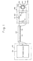
- FIG. 1 is a schematic circuit diagram showing a conventional RF discharge excitation laser apparatus.
- the conventional RF discharge excitation laser apparatus comprises an RF power source 101, a coaxial cable 103, a matching circuit 102, and a laser tube 104.
- the RF power source 101 is arranged in a power source unit (power source portion) 105 used for outputting an RF voltage to the laser tube 104.
- An output voltage of the RF power source 101 is applied to the matching circuit 102 arranged in a laser output unit 106 through the coaxial cable 103.
- the coaxial cable 103 is inserted between the RF power source 101 and the matching circuit 102 because a characteristic impedance of the coaxial cable is 50 ⁇ to 75 ⁇ and a perfect match cannot be established unless the coaxial cable is connected to the output side of the RF power source 101 having a low impedance.
- the matching circuit 102 matches an output impedance Z 0 ' of the RF power source 101 through the coaxial cable 103 with an impedance Z L ' of the laser tube 104, so that the output voltage of the RF power source 101 can be effectively transmitted to the laser tube 104.
- the matching circuit 102 is a ⁇ matching circuit comprising a capacitor 121 connected in parallel with an internal conductor 131 and an external conductor 132, a capacitor 123 connected to two electrodes 143a and 143b of the laser tube, and a coil 122 connected in series between the internal conductor 131 of the coaxial cable and the electrode 143a of the laser tube.
- a discharge occurs in an interior 142 of a ceramic tube 141 upon application of an RF voltage to the electrodes 143a and 143b, and carbon dioxide gas in the interior 142 of the ceramic tube is excited by this discharge. That is, in this RF discharge excitation laser apparatus, CO 2 molecules are excited to a high level vibration state, light emitted by the CO 2 molecules is reflected and resonated by two parallel reflecting mirrors arranged on both sides of the laser tube 104, and part of the light is extracted as a laser output.
- the laser output unit 106 including the laser tube 104 and the matching circuit 102 is located, for example, at an arm portion of an industrial robot.
- the RF power source 101 arranged in the power source unit 105 and the matching circuit 102 in the laser output unit 106 located, for example, at an arm portion of an industrial robot must be adjusted, and therefore, a maintenance problem arises.
- the matching circuit 102 When the matching circuit 102 is arranged at the position of the laser tube 104, a loop for generating noise is enlarged, and the exterior of the laser output unit 106 must be completely shielded to block this noise.
- the structure of the arm position of the industrial robot including the laser output unit 106 becomes heavy and complicated.
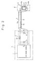
- FIG. 2 is a schematic circuit diagram showing a first example of an RF discharge excitation laser apparatus not according to the present invention.
- a voltage having a frequency of several MHz is applied between two electrodes 43a and 43b of a laser tube 4, to obtain a laser output.
- the laser apparatus mainly comprises an RF power source 1, a matching circuit 2, a coaxial cable 3, and the laser tube 4.
- the RF power source 1 is arranged in a power source unit (power source portion) 5 and outputs an RF voltage of several hundreds of volts. This output voltage is applied to the input of the matching circuit 2 arranged in the power source unit 5.
- the output of the matching circuit 2 is connected to one end of the coaxial cable 3, and the other end of the coaxial cable 3 is connected to the laser tube 4.
- the matching circuit 2 is, for example, a ⁇ matching circuit comprising a capacitor 21 connected in parallel with the outputs of the RF power source 1, a capacitor 23 connected in parallel with an internal conductor 31 and an external conductor 32 in the coaxial cable 3, and a coil 22 connected in series between one output of the RF power source 1 and the internal conductor 31 of the coaxial cable 3.
- the ⁇ matching circuit 2 is arranged in the power source unit 5 including the RF power source 1. Accordingly, if the RF discharge excitation laser apparatus must be adjusted due to deterioration over a period of time, only the power source unit 5 side need be disassembled to adjust the laser.
- the matching circuit 2 is arranged to match an output impedance Z 0 of the RF power source 1 with an impedance Z L of the laser tube 4 through the coaxial cable 3.
- the impedance Z L is changed in the range of, for example, 500 ⁇ to 3 K ⁇ , in accordance with an output state of the laser beam.
- the impedance Z L of the laser tube 4 cannot be perfectly matched with an output impedance Z 1 of the matching circuit 2, and in addition, a characteristic impedance Z W of the coaxial cable 3 is, for example, 50 ⁇ or 75 ⁇ , and is greatly different from the impedance Z L of the laser tube 4.
- the laser tube 4 is arranged in a laser output unit (laser emitting portion) 6 and comprises a tube 41 made of quartz glass and the electrodes 43a and 43b arranged at the upper and lower ends of the quartz glass tube 41.
- the output voltage of the RF power source 1 is boosted by the matching circuit 2 and is applied to the electrodes 43a and 43b of the laser tube 4 through the coaxial cable 3.
- An RF discharge occurs in an interior 42 of the quartz glass tube 41 due to the RF voltage applied to electrodes 43a and 43b of the laser tube, and this glow discharge causes an excitation of carbon dioxide gas (a gas mixture of CO 2 , N 2 , and He in practice) in the interior 42 of the quartz glass tube.
- CO 2 molecules in the interior 42 of the quartz glass tube are excited to a high level vibration state.
- CO 2 molecules emit light having two parallel reflecting mirrors (not shown) arranged on both sides of the laser tube 4, and part of the light is extracted as a laser output.
- a noise loop is limited to connection portion between the electrodes 43a, 43b of the laser tube 4 and coaxial cable 3, and accordingly, noise is rarely generated by the laser output unit 6, and thus the exterior of the laser output unit 6 need not be completely shielded. Therefore, for example, the arm portion of the industrial robot including the laser output unit 6, does not need a complex structure.
- Figure 3 is a schematic circuit diagram showing a modification of the example of the RF discharge excitation laser apparatus shown in Fig. 2.
- the RF discharge excitation laser apparatus shown in Fig. 3 uses a coaxial cable 3 as the capacitor 23 in the matching circuit 2 of the RF discharge excitation laser apparatus shown in Fig. 2.
- the length of the coaxial cable 3 is 1.5 meters, and the capacitance thereof is 150 pF, it is assumed that a 150-pF capacitor 23 is connected to a laser tube 4, and the values of a capacitor 21 and a coil 22 in the matching circuit 2 are determined by this assumption.
- a capacitance Q 2 on the laser tube 4 side of the matching circuit 2 can be minimized.
- an output impedance Z 0 of an RF power source 1 is small, an impedance Z L of the laser tube 4 is large, and a high voltage is applied to the laser tube 4, and under these conditions, a capacitance Q 1 of the capacitor 21 in the matching circuit 2 can be effectively decreased.
- the capacitor 21 having a large capacitance Q 1 and a high breakdown voltage cannot be easily obtained, but if the coaxial cable 3 is used as the capacitor 23 in the matching circuit 2, the capacitance Q 1 of the capacitor 21 can be reduced, compared with the case wherein the capacitor 23 is arranged in the matching circuit 2, as in the embodiment of Fig. 2.
- the arrangement and operation of the RF discharge excitation laser apparatus according to this example are the same as those of the example shown in Fig. 2, and thus a detailed description thereof will be omitted.
- the matching circuit is arranged in the power source unit including the RF power source, and the output of the matching circuit is connected to the laser tube through the coaxial cable. Therefore, the maintenance and structure of the laser tube location can be simplified, and the weight and the number of components of the laser apparatus can be reduced, thereby improving the reliability of the laser.
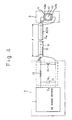
- FIG. 4 is a schematic circuit diagram showing a second example of an RF discharge excitation laser apparatus not according to the present invention.
- a voltage having a frequency of, for example, several MHz is applied between two electrodes 43a and 43b of a laser tube 4 to obtain a laser output.
- the laser apparatus mainly comprises an RF power source 1, a matching circuit 2, a coaxial cable 3, and the laser tube 4.
- the RF power source 1 is arranged in a power source unit 5 and outputs an RF voltage of, for example, several hundreds of volts.
- a capacitor 21 is connected in parallel with the output terminals of the RF power source 1, and a coil 22 is connected in series with one of the output terminals.
- One end of an internal conductor 31 and one end of an external conductor 32 of the coaxial cable 3 are connected to one output terminal of the RF power source 1 through the coil 22 and the other output terminal thereof, respectively.
- a coil 23 is connected in parallel with one output terminal of the RF power source 1 through the coil 22 and the other output terminal thereof.
- the other end of the internal conductor 31 and the other end of the external conductor 32 of the coaxial cable 3 are connected to the electrodes 43a and 43b of the laser tube 4, respectively, and thus an output voltage of the RF power source 1 is applied to the laser tube 4.
- the matching circuit 2 for matching the RF power source 1 with the laser tube 4 is a ⁇ matching circuit comprising the capacitor 21 connected in parallel with outputs of the RF power source 1, the coil 22 connected in series between one output terminal of the RF power source 1 and the internal conductor 31 of the coaxial cable 3, the coil 23 connected to the internal and external conductors 31 and 32 of the coaxial cable 3, and an electrostatic capacitance Q 2 of the coaxial cable 3.
- the electrostatic capacitance Q 2 of the coaxial cable 3 having a length l is reduced by the coil 23, and thus an electrostatic capacitance Q 1 of the capacitor 21 can be reduced.
- the matching circuit 2 when the length l of the coaxial cable 3 is increased, the electrostatic capacitance Q 2 of the coaxial cable 3 is increased. Therefore, the inductance of the coil 23 must be increased in accordance with the length of coaxial cable 3.
- the output voltage from the RF power source 1 can be satisfactorily boosted, and an impedance Z 0 of the RF power source 1 can be accurately matched with an impedance Z L of the laser tube 4 through the coaxial cable 3, and consequently, the output power of the RF power source 1 can be effectively supplied to the laser tube 4.
- the distance l of the coaxial cable 3 having a characteristic capacitance of about 100 pF/meter is given as 3 meters (the electrostatic capacitance Q 2 of the coaxial cable 3 is about 300 pF), and the inductance of the coil 23 is set to be 30 ⁇ H.
- the electrostatic capacitance Q 1 of the capacitor 21 in the matching circuit 2 can be set to 2,000 pF, and therefore, the impedance Z 0 of the RF power source can be accurately matched with the impedance Z L of the laser tube 4 through the coaxial cable 3, and thus the output power from the RF power source 1 can be effectively supplied to the laser tube 4.
- the impedance Z L of the laser tube 4 is, in practice, changed over the range of 500 ⁇ to 3 k ⁇ , in accordance with an operating state of the RF discharge excitation laser apparatus. Accordingly, the impedance Z L of the laser tube 4 is not always matched with an output impedance of the matching circuit 2 including the electrostatic capacitance Q 2 of the coaxial cable, but a perfect match can be established for an operating point of the normally operated laser tube 4.
- a characteristic impedance Z w of the coaxial cable 3 is, for example, 50 ⁇ or 75 ⁇ , and is greatly different from the impedance Z L of the laser tube 4, but even if an RF voltage is reflected from the laser tube 4 to the matching circuit 2 through the coaxial cable 3 when a perfect match between the output impedance Z L of the laser tube 4, and the output impedance of the matching circuit 2 and the characteristic impedance Z W of the coaxial cable 3 is not established, the reflected RF voltage is reflected again to the laser tube 4 through the coaxial cable 3, and therefore, the output power of the RF power source 1 can be supplied to the laser tube 4 with a high efficiency, and thus no significant problems arise.
- a noise loop is limited to connection portions between the electrodes 43a and 43b of the laser tube 4 and the coaxial cable 3, and accordingly, noise is rarely generated by the laser output unit 6, and thus the exterior of the laser output unit 6 does not need to be completely shielded. Therefore, for example, the arm portion of the industrial robot including the laser output unit 6 does not need a complex structure.
- the inductance element is connected to the RF power source side of the coaxial cable, the electrostatic capacitance of the coaxial cable is reduced by the inductance element, and the capacitance of the capacitance element connected in parallel with the output terminals of the RF power source can be reduced. Therefore, the compact matching circuit can accurately match the RF power source with the laser tube through the coaxial cable.
- FIG. 5 is a schematic circuit diagram showing an embodiment of an RF discharge excitation laser apparatus according to the present invention.
- reference numeral 1 denotes an RF current inverter as the RF power source.
- the current inverter 1 comprises a choke coil L 0 inserted in series with the inverter circuit, and four switching N-channel MOS (Metal-Oxide-Semiconductor) transistors 11, 12, 13, and 14.
- the choke coil L 0 is used to maintain an input current I S and acts as a DC power portion to obtain a constant current power source.
- a switching circuit is obtained by a parallel connection with the choke coil L 0 .
- the switching circuit comprises a series circuit of transistors 11 and 12, and a series circuit of the transistors 13 and 14.
- a connecting point between the transistors 11 and 12 is connected to an output terminal 1a, and a connecting point between the transistors 13 and 14 is connected to an output terminal 1b.
- Drive voltages V G , V G , V G , and V G having the same frequency f 0 are input to the gates of the transistors 11 to 14, respectively, and the pair of transistors 11 and 14 and the pair of transistors 12 and 13 are alternately turned ON/OFF in accordance with the frequency f 0 of the drive signal.
- An RF voltage corresponding to the frequency f 0 appears between the output terminals 1a and 1b.
- Reference numeral 8 denotes a parallel resonance circuit (tank circuit).
- the current inverter circuit 1 and the tank circuit 8 are arranged in a power source unit 5.
- Reference numeral 3 denotes a coaxial cable for electrically connecting the power source side to the load side.
- One output terminal 1a of a current inverter 1 is connected to one input terminal 6a (load side) of a laser output unit 6 through a central conductor 31 of the coaxial cable, and the other output terminal 1b of the power source 1 is connected to the other input terminal 6b of the laser output unit 6 through an external conductor 32.
- Reference numeral 4 denotes a laser tube, and the laser tube 4 comprises a pair of electrodes 43a and 43b to which an RF voltage is applied, and a tube, for example, a quartz tube 41, used for the discharge.
- a ⁇ matching circuit 7 is inserted between the electrodes 43a and 43b and the input terminals 6a and 6b.
- the matching circuit 7 includes a coil 72 at the central portion thereof and capacitors 71 and 72 at both ends thereof.
- the ⁇ matching circuit 7 matches an impedance Z 2 obtained, when viewed from the terminals 6a and 6b to the power source side, with an impedance Z L between the electrodes 43a and 43b of the laser tube 4. Therefore, unless the impedance is changed between the power source 1 and the laser tube 6, the RF output voltage of the power source 1 can be effectively transmitted to the laser tube 6.
- the tank circuit 8 when the tank circuit 8 is operated in the parallel resonance mode, for example, when the RF signal having the frequency f 0 appears between the output terminals 1a and 1b of the inverter circuit 1, an impedance Z 0 obtained, when viewed from the terminals 1a and 1b to the power source side, is determined by the impedance of the tank circuit 8. Even if the impedance in the load side from the output terminals 1a and 1b occurs after the installation position of the power source or laser tube is changed or the cable layout is changed, the change will be small enough to be ignored compared with the impedance of the tank circuit 8 itself.
- the power source is not adversely affected by a change in impedance, and this indicates that a degradation of the matching circuit 7, which is caused by a load variation, does not adversely affect the power operation. Therefore, unlike the conventional apparatus, the parameters of respective elements in the matching circuit need not be precisely adjusted, or a perfect match need not be established, and therefore, complex adjustment operations can be omitted.
- FIG. 6 is a schematic circuit diagram showing another example of an RF discharge excitation laser apparatus not according to the present invention.
- this example of an RF discharge excitation laser apparatus not according to the present invention is arranged such that a voltage of, for example, several MHz, is applied between two electrodes 43a and 43b of a laser tube 4 to obtain a laser output.
- the laser apparatus of this embodiment mainly comprises an RF power source 1, a boosting transformer 9, a matching circuit 2, and the laser tube 4.
- the RF power source 1 outputs an RF voltage of several hundreds of volts, and this output voltage is applied to a primary winding 91 of the boosting transformer 9.
- the matching circuit 2 is connected to a secondary winding 92 of the boosting transformer 9.
- the output voltage generated by the RF power source 1 and boosted by the boosting transformer 9 is applied to the secondary winding 92 of the boosting transformer 9, and an input impedance Z 3 of the primary winding 91 of the boosting transformer 9 is matched with an output impedance Z 0 of the RF power source 1, and thus the output of the RF power source 1 can be supplied with high efficiency.
- the boosting transformer 9 can be a compact boosting transformer having a small volume, since the frequency of the voltage for driving the laser tube 4 is a high frequency of, for example, several MHz.
- the matching circuit 2 is a ⁇ matching circuit comprising a capacitor 21 connected in parallel with the outputs of the RF power source 1, a capacitor 23 connected to the two electrodes 43a and 43b of the laser tube (connected in parallel with the laser tube 4), and a coil 22 connected in series between one output of the RF power source 1 and the electrode 43a of the laser tube.
- the ⁇ matching circuit 2 since the capacitances of the capacitors 21 and 23 are properly set, the laser tube 4 can be stably driven, and an input impedance Z 5 of the matching circuit 2 is matched with an output impedance Z 4 of the secondary winding 92 of the boosting transformer 9, thus preventing unnecessary power loss.
- the matching circuit 2 matches the output impedance Z 4 of the secondary winding 92 of the boosting transformer 9 with an impedance Z L of the laser tube 4.
- An output voltage generated from the RF power source 1 is boosted by the boosting transformer 9 (for example, boosted 2 to 5 times), and the boosted voltage is applied between the two electrodes 43a and 43b of the laser tube 4.
- the impedance Z L of the laser tube 4 varies in the range of, for example, 500 ⁇ to 3 k ⁇ , in accordance with an output state of the laser beam.
- the impedance Z L of the laser tube 4 cannot be perfectly matched with an output impedance Z 6 of the matching circuit 2, but even if perfect match between the impedance Z L of the laser tube 4 and the output impedance Z 6 of the matching circuit 2 is not established and the RF voltage is reflected to the matching circuit 2, the reflected RF voltage is reflected to the laser tube 4 again, and therefore, the power output from the RF power source 1 can be supplied to the laser tube 4 with a high efficiency.
- the boosting transformer is arranged between the RF power source and the matching circuit to boost the output voltage from the RF power source, the output voltage of the RF power source is boosted by both the boosting transformer and the matching circuit, and the boosted voltage is then applied to the laser tube. Therefore, the area occupied by the circuit can be reduced due to a simple circuit arrangement, and a stable laser beam can be generated with a high efficiency.
- FIG. 7 is a schematic circuit diagram showing another example of an RF discharge excitation laser apparatus not according to the present invention.
- a ⁇ matching circuit 2 is connected between an RF power source 1 and a laser tube 4.
- the ⁇ matching circuit 2 comprises input and output capacitive elements (condensers) 21 and 23 (the capacitance thereof being C 1 and C 2 , respectively) and an inductance element 22 having an inductance L.
- the impedance Z L of the laser tube 4 is not limited before an RF voltage is applied or prior to discharge, but when the RF voltage is applied to both electrodes 43a and 43b of the laser tube, and the discharge is started, the initial impedance is set to be, for example, about 3 k ⁇ . As the power injection progresses, the operating point impedance at the time of operation is decreased to, for example, about 500 ⁇ . In this manner, the impedance Z L of the laser tube 4 greatly varies from the state prior to discharge to the operating state at an operating point.
- the Q value falls within the range of about 3 to 5.
- FIG. 8 shows a curve showing efficiency variations caused by changes in the load impedance Z S .
- a Q value is small, variations in efficiency ⁇ caused by changes in the load impedance are moderate, taking the matching point (point of the load impedance Z S0 ) as the center, as indicated by a curve B.
- the efficiency ⁇ varies slightly.
- the Q value is set to be relatively small (that is, about 3 to 5), in consideration of a small matching error.
- the load impedance Z L is not limited prior to discharge (nonload state), as described above, and when the discharge is started, the load impedance Z L is abruptly decreased. That is, the load impedance is reduced to about 500 ⁇ at the operating point, and thus, during the discharge operation, the load impedance Z L is greatly changed.
- the Q value is set to be about 3 to 5 in the conventional matching circuit, to establish a match at the operating point.
- the load impedance Z L prior to discharge is not limited, and as long as a match at the operating point is established by one matching circuit, a large matching error occurs and thus a discharge will not occur when a predetermined power source voltage is applied.
- a plurality of matching circuits are used, the power source voltage is boosted, or a pulse is superimposed on the power source voltage.
- a gas pressure of the laser tube is decreased in order to decrease the discharge start voltage.
- the example shown in Fig. 7 of an RF discharge excitation laser apparatus not according to the present invention is arranged to determine respective constants of the matching circuit such that the Q value used in the conventional technique is decreased (2 or less in practice) to facilitate the start of discharge upon application of the power source voltage, in order to improve the start characteristics, and that after the start of discharge, an operating point corresponding to a predetermined current command value is obtained and an automatic match is performed at the operating point.
- the value of a constant Q required for setting the input capacitance C 1 is set to be 2 or less.
- Figure 9 shows the relationship between the Q value and a boosting ratio V 2 /V 1 (where V 1 is an output voltage of the RF power source 1 and V 2 is a voltage applied to the laser tube 4) prior to the start of a discharge of the laser tube (that is, in a state wherein an impedance Z L of the laser tube 4 is not limited).
- V 1 is an output voltage of the RF power source 1
- V 2 is a voltage applied to the laser tube 4
- the boosting ratio V 2 /V 1 is abruptly increased.
- the discharge of the laser tube could not be smoothly started unless the Q value was at least 2 or less. This was found as a result of experimental and theoretical studies on AC discharge characteristics by the present inventor.
- the boosting ratio at the time of application of the power source voltage is increased to smoothly start the discharge of the laser tube 4.
- the output capacitance C 2 and the inductance L of the matching circuit 2 are set by equations (2) and (3) using the Q value of 2 or less, and the Z 0 and Z L values (that is, the load impedance values at the operating point):
- the matching circuit 7 is exemplified by an ⁇ matching circuit, but the matching circuit 7 in the RF discharge excitation laser apparatus according to other embodiments of the present invention is not limited to such a matching circuit. Further, the RF discharge excitation laser apparatus according to the present invention is not limited to a carbon dioxide layer, but is also applicable to any other gas laser such as an He-Ne gas laser, a CO (carbon monoxide) gas laser, and an excimer laser.
Landscapes
- Physics & Mathematics (AREA)
- Electromagnetism (AREA)
- Engineering & Computer Science (AREA)
- Plasma & Fusion (AREA)
- Optics & Photonics (AREA)
- Lasers (AREA)
Claims (3)
- HF-Entladungsanregungs-Laservorrichtung mit einem Spannungsquellenabschnitt (5), einem laseraussendenden Abschnitt (6) und einer Spannungsübertragungseinrichtung (3) für die Übertragung von Spannung, die durch den Spannungsquellenabschnitt erzeugt wird, zu dem laseraussendenden Abschnitt, wobei die HF-Entladungsanregungs-Laservorrichtung aufweist:eine Hochfrequenz-Spannungsquelle (1), die in dem Spannungsquellenabschnitt angeordnet ist und zum Erzeugen einer Hochfrequenzspannung dient,eine Laserröhre (4), die in dem laseraussendenden Abschnitt angeordnet ist und zum Aussenden eines Laserstrahls dient, undeine Anpassungseinrichtung (8), die in dem Spannungsquellenabschnitt angeordnet ist und zum Anpassen einer Ausgangsimpedanz der Hochfrequenz-Spannungsquelle an eine Impedanz der Laserröhre, die über die Spannungsübertragungseinrichtung angeschlossen ist, dient,dadurch gekennzeichnet, daß
die Anpassungseinrichtung eine Parallelresonanzschaltung enthält, die an Ausgangsanschlüsse der Hochfrequenz-Spannungsquelle angeschlossen ist, wobei die Parallelresonanzschaltung derart betrieben wird, daß die Impedanz, wenn sie von den Ausgangsanschlüssen der Hochfrequenz-Spannungsquelle zu der Laserröhre gesehen wird, dazu gebracht ist, im wesentlichen lediglich eine Widerstandskomponente zu sein. - Vorrichtung nach Anspruch 1, bei dem die Hochfrequenz-Spannungsquelle (1) eine Stromwechselrichterschaltung aufweist.
- Vorrichtung nach Anspruch 1, bei dem der laseraussendende Abschnitt (6) ebenfalls eine Anpassungsschaltung (7) für die Anpassung der Ausgangsimpedanz der Laserröhre (4) an die Ausgangsimpedanz der Hochfrequenz-Spannungsquelle, die über die Spannungsübertragungseinrichtung (3) angeschlossen ist, aufweist.
Applications Claiming Priority (11)
| Application Number | Priority Date | Filing Date | Title |
|---|---|---|---|
| JP242074/86 | 1986-10-14 | ||
| JP24207286A JPS6396976A (ja) | 1986-10-14 | 1986-10-14 | 高周波放電励起レ−ザ |
| JP61242074A JP2739936B2 (ja) | 1986-10-14 | 1986-10-14 | 高周波放電励起レーザ |
| JP242072/86 | 1986-10-14 | ||
| JP24320486A JPH0770772B2 (ja) | 1986-10-15 | 1986-10-15 | 高周波放電励起レ−ザ装置 |
| JP243204/86 | 1986-10-15 | ||
| JP243211/86 | 1986-10-15 | ||
| JP24321186A JPH0770774B2 (ja) | 1986-10-15 | 1986-10-15 | 交流放電励起レ−ザ装置 |
| JP267722/86 | 1986-11-12 | ||
| JP26772286A JPH0770775B2 (ja) | 1986-11-12 | 1986-11-12 | 高周波放電励起レ−ザ |
| EP87906762A EP0285673B1 (de) | 1986-10-14 | 1987-10-14 | Hf-entladungsangeregte laservorrichtung |
Related Parent Applications (2)
| Application Number | Title | Priority Date | Filing Date |
|---|---|---|---|
| EP87906762.7 Division | 1987-10-14 | ||
| EP87906762A Division-Into EP0285673B1 (de) | 1986-10-14 | 1987-10-14 | Hf-entladungsangeregte laservorrichtung |
Publications (2)
| Publication Number | Publication Date |
|---|---|
| EP0592014A1 EP0592014A1 (de) | 1994-04-13 |
| EP0592014B1 true EP0592014B1 (de) | 1997-07-02 |
Family
ID=27530064
Family Applications (2)
| Application Number | Title | Priority Date | Filing Date |
|---|---|---|---|
| EP87906762A Expired - Lifetime EP0285673B1 (de) | 1986-10-14 | 1987-10-14 | Hf-entladungsangeregte laservorrichtung |
| EP93119934A Expired - Lifetime EP0592014B1 (de) | 1986-10-14 | 1987-10-14 | HF Entladungsangeregter Laser-Apparat |
Family Applications Before (1)
| Application Number | Title | Priority Date | Filing Date |
|---|---|---|---|
| EP87906762A Expired - Lifetime EP0285673B1 (de) | 1986-10-14 | 1987-10-14 | Hf-entladungsangeregte laservorrichtung |
Country Status (4)
| Country | Link |
|---|---|
| US (1) | US4975920A (de) |
| EP (2) | EP0285673B1 (de) |
| DE (2) | DE3750578T2 (de) |
| WO (1) | WO1988002936A1 (de) |
Families Citing this family (8)
| Publication number | Priority date | Publication date | Assignee | Title |
|---|---|---|---|---|
| DE3825871A1 (de) * | 1988-07-29 | 1990-02-01 | Leybold Ag | Einrichtung fuer die anregung des gases eines gaslasers |
| US5008894A (en) * | 1990-03-30 | 1991-04-16 | Synrad, Incorporated | Drive system for RF-excited gas lasers |
| US9012807B2 (en) * | 2004-04-16 | 2015-04-21 | Illinois Tool Works Inc. | Remote wire feeder using binary phase shift keying to modulate communications of command/control signals to be transmitted over a weld cable |
| US7180029B2 (en) | 2004-04-16 | 2007-02-20 | Illinois Tool Works Inc. | Method and system for a remote wire feeder where standby power and system control are provided via weld cables |
| DE102004039082A1 (de) * | 2004-08-12 | 2006-02-23 | Trumpf Laser- Und Systemtechnik Gmbh | Anordnung mit einem HF-angeregten Laserresonator |
| CN100483870C (zh) * | 2006-12-25 | 2009-04-29 | 江苏新潮科技集团有限公司 | 射频板条co2激光器匹配系统可变电容器的自动调节装置及方法 |
| US7540779B2 (en) * | 2007-03-23 | 2009-06-02 | Coherent, Inc. | RF shielded, series inductor, high RF power impedance matching interconnector for CO2 slab laser |
| CN101640369B (zh) * | 2009-08-25 | 2011-05-25 | 深圳市大族激光科技股份有限公司 | 一种射频电源装置 |
Family Cites Families (13)
| Publication number | Priority date | Publication date | Assignee | Title |
|---|---|---|---|---|
| JPS458896Y1 (de) * | 1966-10-15 | 1970-04-25 | ||
| JPS4951158U (de) * | 1972-08-11 | 1974-05-07 | ||
| US4112392A (en) * | 1975-09-17 | 1978-09-05 | Andersson Hans E B | Method and apparatus for producing laser pulses with high reproducibility |
| JPS55156532A (en) * | 1979-05-25 | 1980-12-05 | Sudo Sukenao | Transporting vehicle for use with selffrunning feeding vehicle |
| JPS55160485A (en) * | 1979-06-01 | 1980-12-13 | Mitsubishi Electric Corp | Silent discharge type laser |
| US4373202A (en) * | 1979-09-24 | 1983-02-08 | Walwel, Inc. | RF Excited waveguide gas laser |
| US4352188A (en) * | 1980-07-03 | 1982-09-28 | Hughes Aircraft Company | rf Pumped waveguide laser with inductive loading for enhancing discharge uniformity |
| JPS582087A (ja) * | 1981-06-26 | 1983-01-07 | Toshiba Corp | ガス・レ−ザ管装置 |
| JPS5848980A (ja) * | 1981-09-18 | 1983-03-23 | Mitsubishi Electric Corp | 無声放電励起レ−ザ−装置 |
| DE3240372A1 (de) * | 1982-11-02 | 1984-05-03 | Kraftwerk Union AG, 4330 Mülheim | Anregungssystem zur erzeugung einer schnellen, gepulsten hochspannungsentladung, insbesondere zur anregung eines hochleistungslasers |
| US4618961A (en) * | 1982-12-16 | 1986-10-21 | Sutter Jr Leroy V | Configuration of electrodes for transversely excited gas lasers |
| JPS60177692A (ja) * | 1984-02-24 | 1985-09-11 | Mitsubishi Electric Corp | レ−ザ発振装置 |
| US4761786A (en) * | 1986-12-23 | 1988-08-02 | Spectra-Physics, Inc. | Miniaturized Q-switched diode pumped solid state laser |
-
1987
- 1987-10-14 EP EP87906762A patent/EP0285673B1/de not_active Expired - Lifetime
- 1987-10-14 WO PCT/JP1987/000771 patent/WO1988002936A1/ja active IP Right Grant
- 1987-10-14 EP EP93119934A patent/EP0592014B1/de not_active Expired - Lifetime
- 1987-10-14 DE DE3750578T patent/DE3750578T2/de not_active Expired - Fee Related
- 1987-10-14 DE DE3752083T patent/DE3752083T2/de not_active Expired - Fee Related
-
1990
- 1990-03-30 US US07/503,149 patent/US4975920A/en not_active Expired - Fee Related
Also Published As
| Publication number | Publication date |
|---|---|
| DE3750578T2 (de) | 1995-02-09 |
| DE3750578D1 (de) | 1994-10-27 |
| EP0285673B1 (de) | 1994-09-21 |
| EP0285673A4 (de) | 1989-02-13 |
| EP0592014A1 (de) | 1994-04-13 |
| WO1988002936A1 (en) | 1988-04-21 |
| DE3752083D1 (de) | 1997-08-07 |
| DE3752083T2 (de) | 1998-02-12 |
| US4975920A (en) | 1990-12-04 |
| EP0285673A1 (de) | 1988-10-12 |
Similar Documents
| Publication | Publication Date | Title |
|---|---|---|
| KR100522221B1 (ko) | 압전 트랜스의 구동 회로, 냉음극관 발광 장치, 액정 패널및 액정 패널 장착 기기 | |
| KR100497973B1 (ko) | 압전 트랜스의 구동회로 및 구동방법, 백 라이트 장치,액정표시장치, 액정 모니터 및 액정 텔레비전 | |
| EP1814367B1 (de) | Rücklicht-inverter und verfahren zu seiner ansteuerung | |
| US4837772A (en) | Electrically self-oscillating, rf-excited gas laser | |
| EP1220580B1 (de) | Anordnung und Verfahren zum Steuern einer Kaltkathoden -Entladungslampe | |
| US6737816B2 (en) | Piezoelectric transformer, piezoelectric transformer drive circuit, piezoelectric transformer drive method and cold cathode tube drive apparatus using piezoelectric transformer | |
| EP0592014B1 (de) | HF Entladungsangeregter Laser-Apparat | |
| WO1991015884A1 (en) | Improved drive system for rf-excited gas lasers | |
| EP0294492B1 (de) | Hf-entladungsangeregter laser | |
| EP1986475B1 (de) | Zündschaltung für eine HID-Lampe | |
| EP0285674B1 (de) | Wechselrichter | |
| EP0312613A1 (de) | Laser-oszillator | |
| JP3271377B2 (ja) | インバータ回路及びこれを用いた無電極放電ランプ点灯装置 | |
| JP2001275343A (ja) | 圧電トランス、圧電トランスの駆動回路、圧電トランスの駆動方法及び、圧電トランスを用いた冷陰極管駆動装置 | |
| KR20020062571A (ko) | 필라멘트 가열의 작동중지기를 부착한 기체 방전등용안정기 | |
| JP2739936B2 (ja) | 高周波放電励起レーザ | |
| JP2996706B2 (ja) | パルスレーザ発振装置 | |
| JP3819502B2 (ja) | レーザ発振器用高周波電源装置 | |
| JPH0770775B2 (ja) | 高周波放電励起レ−ザ | |
| JPH10335084A (ja) | インバータトランス | |
| JP3409472B2 (ja) | 無電極放電灯点灯装置 | |
| JPH09129952A (ja) | 高周波放電励起ガスレーザーの放電回路 | |
| JPS6396976A (ja) | 高周波放電励起レ−ザ | |
| JPH1079541A (ja) | レーザ電源装置 | |
| JPH0413872B2 (de) |
Legal Events
| Date | Code | Title | Description |
|---|---|---|---|
| PUAI | Public reference made under article 153(3) epc to a published international application that has entered the european phase |
Free format text: ORIGINAL CODE: 0009012 |
|
| AC | Divisional application: reference to earlier application |
Ref document number: 285673 Country of ref document: EP |
|
| AK | Designated contracting states |
Kind code of ref document: A1 Designated state(s): DE FR GB |
|
| 17P | Request for examination filed |
Effective date: 19940930 |
|
| GRAG | Despatch of communication of intention to grant |
Free format text: ORIGINAL CODE: EPIDOS AGRA |
|
| 17Q | First examination report despatched |
Effective date: 19960805 |
|
| GRAH | Despatch of communication of intention to grant a patent |
Free format text: ORIGINAL CODE: EPIDOS IGRA |
|
| GRAH | Despatch of communication of intention to grant a patent |
Free format text: ORIGINAL CODE: EPIDOS IGRA |
|
| GRAA | (expected) grant |
Free format text: ORIGINAL CODE: 0009210 |
|
| AC | Divisional application: reference to earlier application |
Ref document number: 285673 Country of ref document: EP |
|
| AK | Designated contracting states |
Kind code of ref document: B1 Designated state(s): DE FR GB |
|
| PG25 | Lapsed in a contracting state [announced via postgrant information from national office to epo] |
Ref country code: FR Effective date: 19970702 |
|
| REF | Corresponds to: |
Ref document number: 3752083 Country of ref document: DE Date of ref document: 19970807 |
|
| EN | Fr: translation not filed | ||
| PLBE | No opposition filed within time limit |
Free format text: ORIGINAL CODE: 0009261 |
|
| STAA | Information on the status of an ep patent application or granted ep patent |
Free format text: STATUS: NO OPPOSITION FILED WITHIN TIME LIMIT |
|
| 26N | No opposition filed | ||
| PGFP | Annual fee paid to national office [announced via postgrant information from national office to epo] |
Ref country code: DE Payment date: 20001009 Year of fee payment: 14 |
|
| PGFP | Annual fee paid to national office [announced via postgrant information from national office to epo] |
Ref country code: GB Payment date: 20001011 Year of fee payment: 14 |
|
| PG25 | Lapsed in a contracting state [announced via postgrant information from national office to epo] |
Ref country code: GB Free format text: LAPSE BECAUSE OF NON-PAYMENT OF DUE FEES Effective date: 20011014 |
|
| REG | Reference to a national code |
Ref country code: GB Ref legal event code: IF02 |
|
| GBPC | Gb: european patent ceased through non-payment of renewal fee |
Effective date: 20011014 |
|
| PG25 | Lapsed in a contracting state [announced via postgrant information from national office to epo] |
Ref country code: DE Free format text: LAPSE BECAUSE OF NON-PAYMENT OF DUE FEES Effective date: 20020702 |