EP0588656B1 - Digitale Schaltung zur Signalflankenpositionsmessung - Google Patents
Digitale Schaltung zur Signalflankenpositionsmessung Download PDFInfo
- Publication number
- EP0588656B1 EP0588656B1 EP93307355A EP93307355A EP0588656B1 EP 0588656 B1 EP0588656 B1 EP 0588656B1 EP 93307355 A EP93307355 A EP 93307355A EP 93307355 A EP93307355 A EP 93307355A EP 0588656 B1 EP0588656 B1 EP 0588656B1
- Authority
- EP
- European Patent Office
- Prior art keywords
- circuit
- output
- edge
- signal
- window
- Prior art date
- Legal status (The legal status is an assumption and is not a legal conclusion. Google has not performed a legal analysis and makes no representation as to the accuracy of the status listed.)
- Expired - Lifetime
Links
Images


Classifications
-
- G—PHYSICS
- G11—INFORMATION STORAGE
- G11B—INFORMATION STORAGE BASED ON RELATIVE MOVEMENT BETWEEN RECORD CARRIER AND TRANSDUCER
- G11B20/00—Signal processing not specific to the method of recording or reproducing; Circuits therefor
- G11B20/10—Digital recording or reproducing
-
- G—PHYSICS
- G01—MEASURING; TESTING
- G01R—MEASURING ELECTRIC VARIABLES; MEASURING MAGNETIC VARIABLES
- G01R25/00—Arrangements for measuring phase angle between a voltage and a current or between voltages or currents
-
- G—PHYSICS
- G01—MEASURING; TESTING
- G01R—MEASURING ELECTRIC VARIABLES; MEASURING MAGNETIC VARIABLES
- G01R29/00—Arrangements for measuring or indicating electric quantities not covered by groups G01R19/00 - G01R27/00
- G01R29/02—Measuring characteristics of individual pulses, e.g. deviation from pulse flatness, rise time or duration
-
- H—ELECTRICITY
- H03—ELECTRONIC CIRCUITRY
- H03L—AUTOMATIC CONTROL, STARTING, SYNCHRONISATION OR STABILISATION OF GENERATORS OF ELECTRONIC OSCILLATIONS OR PULSES
- H03L7/00—Automatic control of frequency or phase; Synchronisation
- H03L7/06—Automatic control of frequency or phase; Synchronisation using a reference signal applied to a frequency- or phase-locked loop
- H03L7/08—Details of the phase-locked loop
- H03L7/10—Details of the phase-locked loop for assuring initial synchronisation or for broadening the capture range
- H03L7/107—Details of the phase-locked loop for assuring initial synchronisation or for broadening the capture range using a variable transfer function for the loop, e.g. low pass filter having a variable bandwidth
Definitions
- This invention relates to a digital phase-locked loop (PLL) circuit and, more particularly, to a digital PLL circuit in which an edge position of the input signal waveform is detected and the PLL operation is performed in a digital fashion based on the detected edge position.
- PLL phase-locked loop
- the PLL circuit is a phase synchronizing circuit in which the phase of an input signal follows the phase of a reference signal.
- An analog PLL circuit is made up of a phase comparator, a low-pass filter and a voltage-controlled oscillator. Recently, there has been proposed a digital PLL circuit in which the operation of the analog PLL circuit is to be performed in a digital fashion.
- the phase difference between the PLL output signal and the input signal is measured using a master clock. That is, the phase difference between the edge of the input signal and the output clock of the PLL circuit is found by the master clock. Based on such phase difference, the output clock is controlled so as to be in phase with the input clock.
- a demand for precision at least one digit higher than the bit clock of the input signal is raised on the master clock.
- the clock frequency of the input signal is increased, it becomes increasingly difficult to select the master clock frequency so as to be higher by at least one digit because the operating clock frequency can not be increased without limitations.
- a demand is raised for a digital PLL circuit which permits facilitated phase difference detection without employing a higher frequency of the master clock.
- the input signals are sampled with the master clocks.
- the timing of the input signal edge, produced by such sampling contains an error dependent on the master clocks. Therefore, for inhibiting data errors in the PLL circuit, it is necessary to sample the input signal with the master clock having as short a period as possible to capture the timing of the input signal edge accurately.
- a PLL circuit has been desired in which a satisfactory error rate may be assured even if the ratio of the master clock frequency/PLL output clock frequency is on the order of 2 or higher.
- JP Patent Publication KOKAI No.63-292825 JP Patent Publication KOKAI No.63-292825
- the output time duration of an N/K number of output clocks of the PLL circuit is sequentially detected and the K number of the sequentially detected time durations is multiplied by 1/N to find the data of the output clock period.
- the digital PLL is constituted using master clocks of a lower frequency.
- the European Application EP-A-0 467 712 discloses a phase detection circuit, in which a reference signal is latched at zero crossings of an input signal, and the outputs of a ring oscillator are latched with the latched reference signal.
- the output PLL clock frequency (reproducing clock frequency) has been increased in keeping up with higher system performance and there is a demand for a master clock frequency to PLL output clock frequency ratio on the order of 2 to 3. Since the error rate tends to be increased with the above techniques, further improvement is desired.
- an input signal edge time measurement circuit comprising a ring oscillator having an odd number of inverters connected in a ring;
- said edge position calculating means comprises third latch means for capturing an output of said first latch means at a rise timing of said master clock and fourth latch means for capturing an output of said first latch means at a decay timing of said master clock, and wherein an output of said third latch means and an output of said fourth latch means are selected when the edge of said input signal is in a high level domain of said master clock and in a low level domain of said master clock, respectively, and the output thus selected is compared to an output of said second latch means by said edge position calculating means.
- said ring oscillator is made up of inverter elements with variable delay and wherein said delay is switchingly selected responsive to the ratio of the period of oscillation of said ring oscillator to the master clock period.
- the circuit for measuring the timing of an input signal edge may be desirably applied to a digital PLL circuit which further comprises:
- the PLL circuit further comprises reproducing clock period detection means for detecting period data of the reproducing clocks from said reproducing clock generating means for transmitting the period data to said reproducing clock generating means.
- the difference in capturing timing by the first and second latch units may be represented by the measurement time unit run. That is, the input signal edge for each master clock period may be represented highly accurately by the measurement time unit run.
- the phase error between the reproducing clock and the input signal edge may be found with the accuracy of the measurement time unit run based on the input edge position represented by the measurement unit run so that optimum FLL operation may be maintained even although the master clock period approaches the reproducing clock period.
- said phase error detection means comprises:
- Fig.1 is a schematic block circuit diagram showing an arrangement of a circuit for measuring the input signal edge timing in a digital PLL circuit according to the present invention.
- Fig.2 is a circuit diagram showing an arrangement of a ring oscillator employed in the PLL circuit shown in Fig.1.
- Fig.3 is a timing chart for illustrating the operation of the ring oscillator shown in Fig.2.
- Fig.4 is a timing chart for illustrating the operation of edge detection of the input signal.
- Fig.5 is a timing chart for illustrating the operation of edge position detection of the input signal.
- Fig.6 is a circuit diagram of an exemplary binary translating circuit.
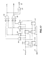
- Fig.7 is a schematic block circuit diagram showing a phase synchronizing circuit of the digital PLL circuit shown in Fig.1.
- Fig.8 shows specific values of signals indicating the edge positions.
- Fig.9 shows the calculation of edge positions for a phase error of 0.
- Fig.10 is a block circuit diagram showing an exemplary window generator in Fig.7.
- Fig.11 illustrates the operation of the window generator shown in Fig.10.
- Fig.12 is a block circuit diagram showing the window circuit of Fig.7 and the peripheral circuitry.
- Fig.13 is a block circuit diagram showing an exemplary circuit for measuring a reproducing clock period.
- Fig.14 is a timing chart for illustrating mistaken detection of the input edge position.
- Fig.15 is a schematic block circuit diagram of a circuit for measuring the edge timing of input signals in a manner free from mistaken detection of the input edge position.
- Fig.16 is a timing chart for illustrating the operation of the circuit shown in Fig.15.
- Fig.17 is a circuit diagram for illustrating a modified embodiment for inhibiting mistaken detection of the input edge position.
- Fig.18 is a timing chart for illustrating the operation of the circuit shown in Fig.17.
- Fig.19 is a block circuit diagram for illustrating an exemplary ring delay time measurement circuit and an exemplary ring delay selection circuit shown in Fig.15.
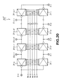
- Fig.20 is a block circuit diagram showing an embodiment of a ring oscillator having delay times selectable by switching.
- Fig.21 is a circuit diagram showing an embodiment of an inverter employed in the ring oscillator having delay times selectable by switching.
- Fig.22 is a schematic block circuit diagram showing a phase synchronizing circuit in which a loop gain switching control means is annexed to the digital PLL circuit according to the present invention.
- Fig.23 illustrates a PLL lock decision signal.
- Fig.1 shows, in a block circuit diagram, arrangement of an input signal edge measurement circuit employed in the digital PLL circuit according to the present invention.
- an RF (high frequency) signal RFin clocks of which are to be reproduced, is supplied to an i-nput terminal 11.
- a master clock signal MCK which is to be a reference signal, is supplied to an input terminal 12.
- the RF input signal RFin is supplied to a data input terminal D of a flip-flop 13, to which the master clock MCK is entered as a clock, so that the input signal RFin is captured at the timing of the master clock.
- An output of the flip-flop 13 and a corresponding signal delayed by one master clock period by the flip-flop 14 are supplied to an exclusive OR circuit 15 for edge detection.
- a detection signal ED timed to the master clock signal MCK, indicating the presence or absence of the input edge, is outputted at an output terminal 16.
- the RF input terminal RFin from input terminal 11 is also supplied to a delay element 21 having a delay time sufficiently shorter than the master clock period TMC and an exclusive-OR circuit 22 for edge detection before being supplied to a clock input terminal of a flip-flop circuit 23.
- the flip-flop circuit 23 is composed of an number n of flip-flops connected in parallel. The number n corresponds to the number of stages n of a ring oscillator 30 which is an odd number, such as 15.
- the flip-flop circuit 23 composed of these n flip-flops, plays the role of capturing the states of the stages of the n-bit ring oscillator 30, consisting of a circular array of n stages of inverters, into each of the data input terminals D thereof depending on the edge detection outputs of the RFin input signal.
- the flip-flop circuit 23 consists of 15 flip-flops connected in parallel for capturing the states of the 15 stages of the inverters making up the ring oscillator 30.
- n is set to 5 for simplicity of the explanation.
- five-stage or five-bit ring oscillator 30' comprises five inverters 31a, 31b, 31c, 31d and 31e connected in a ring. Since number of the inverters is the odd number, there exists an inverter which remains in the same polarity "H" even although the input is changed to "H".
- a two-input NAND gate is employed as element 31a for starting and stopping the oscillation of the ring oscillator 30'.
- the NAND gate 31a has its one terminal supplied with an output signal from the inverter 31e, while having its other terminal supplied with a control signal for controlling the oscillation.
- Fig.3 shows signal waveforms of various parts of the ring oscillator 30' shown in Fig.2.
- the control signal STOP and output signals a , b , c , d and e of the inverters 31a, 31b, 31c, 31d and 31e are shown.
- the delay times of these inverters 31a, 31b, 31c, 31d and 31e are indicated as ⁇ a, ⁇ b, ⁇ c, ⁇ d and ⁇ e, respectively. If the control signal STOP rises, the inverted output signal a from inverter 31a decays after lapse of time ⁇ a.
- the signal inversion occurs sequentially by the subsequent inverters 31b to 31e so that an output signal waveform as shown at (b) to (e) in Fig.3 is produced.
- the period TRN of these output signals depends on the propagation time of the five inverters of the ring oscillator 30'.
- the delay per inverter and the number of stages of the inverters are set so that the period of oscillation TRN of the ring oscillator is longer than the period TMC of the master clock MCK. It is because the timing can not be determined if the same state of the ring oscillator appears more than once during one period of the master clock MCK.
- the signals b , d , a , c and e appear in this order.
- These signals b , d , a , c and e are output as oscillator outputs S1, S2, S3, S4 and S5 at the output terminals 32(1), 32(2), 32(3), 32(4) and 32(5), respectively. It is these output signals S1 to S5 that are supplied to the respective flip-flops making up the flip-flop circuit shown in Fig.1.
- a 15-stage ring oscillator 30, made up of 15 inverters, is employed, and the output signals S1 to S15 of the inverters are supplied to data input terminals D of the 15 flip-flops making up the ring oscillator 30.
- the output signals S1 to S15 of the ring oscillator 30 are captured by the flip-flops at the timing of the RF input signal RFin for performing fine time measurements as later explained, above all, detection of input signal edges with respect to the rising edges of the master clock MCK.
- Fig.4 shows a signal waveform for illustrating the operation of input edge detection for each master clock by the flip-flops 13 and 14 and the exclusive OR 15 shown in Fig.1.
- flip-flop 13 captures the RF input signal RFin from the input terminal 11 of Fig.1 at the rise timing of the master clock signal MCK to output a signal FF13.
- the flip-flop 14 delays the output signal FF13 by a delay time equal to a master clock period TMC to output a signal FF14.
- the exclusive OR 15 takes an exclusive OR of these signals FF13 and FF14 to supply a signal EX15 at an output terminal 16.
- the "H" state of the output signal EX15 represents the state of edge detection at the directly.previous clock period. This enables detection of the possible presence of the input signal edge for each master clock.
- the ring oscillator 30, made up of the 15 inverters, is adapted for measuring the time with the unit time ⁇ un, finer than the master clock MCK, as shown by an output signal RS.
- the time difference d between the rising edge of the master clock MCK and the rising or falling edge of the RF input signal RFin is measured by the ring oscillator output signal RS based on the unit time ⁇ un.
- the master clocks MCK are supplied from the input terminal 1 to the flip-flop circuit 27 made up of a number of flip-flops equal to the number of inverters of the ring oscillator 30 so as to be captured by these flip-flops as clocks.
- the states of the inverters of the ring oscillator 30 are captured by the flip-flops at the timings of the rising edges of the master clocks MCK.
- An example of an output of the flip-flop circuit 27 is shown in Fig.5 as a signal FF27.
- Edge detection of the RF input signal RFin from the input terminal 11 is made by the delay element 21 and the exclusive OR circuit 22 to produce an edge detection signal EX22.
- the edge detection signal EX22 is supplied to a clock input terminal of each flip-flop of the flip-flop circuit 23 so that the states of the inverters of the ring oscillator 30 are captured by the flip-flops at the timing of the edges of the input signal.
- An output signal FF23 of each flip-flop of the flip-flop circuit 23 is supplied to each flip-flop of the next-stage flip-flop circuit 24. Since the master clock MCK is supplied as clock to the flip-flop circuit 24, the signal FF23 is re-captured at the timing of the rising edge of the master clock MCK to produce an output signal FF24 from the flip-flop circuit 24.
- the output signal RS of the ring oscillator shown in Fig.5 is indicated by the numbers 1 to 15 corresponding to the 15 states of the ring oscillator 30 made up of the 15 inverters. That is, these 15 states correspond to the states (15 states) obtained by dividing the period of oscillation of the ring oscillator TRN by the number of the inverters.
- the output signals FF23, FF24 and FF27 of each flip-flop circuit are indicated by the figures corresponding to the inner stages of the ring oscillator 30. For example, the state of the ring oscillator output RS at the rising timing t1 of the master clock MCK i Fig.5 is "1". This state is captured by the 15 flipflops of the flipflop circuit 27. Consequently, the state of the output of the flip-flop circuit 27 since this timing t1 becomes "1".
- the stage of the ring oscillator output RS is "2".
- This state “2” is captured by the flip-flop circuit 23 so that an output becomes “2”.
- This output “2” of the flipflop circuit 23 is captured by the flip-flop circuit 24 at the timing t2 so as to be transmitted to a binary conversion circuit 25.
- the state of the ring oscillator output RS at timing t2 is “9”.
- This state “9” is captured by flip-flop circuit 27 so that an output "9” is transmitted to binary conversion circuit 28.
- These outputs of flip-flop circuits 27, 24 represent output states of the 15 flip-flops. These states are converted by the binary conversion circuits 28, 25 into numerical data BN28, BN25, respectively. In the example of Fig.5, the numerical data "9” and “2” are transmitted to a subtractive unit 26.
- the concrete construction of the binary conversion circuits 28, 25 is explained subsequently by referring to Fig.6.
- the value of the output of the subtractive unit 26 is equivalent to the time duration d1, indicating the fine position of the input signal edge in terms of the unit time ⁇ un.
- the time duration since time point t2 until the rising time t3 of the next master clock MCK is "7" (9 - 2).
- seven flip-flops F1 to F7 correspond to the flip-flop circuits 24 or 27.
- the states of the input signals S1 to S7 are captured by these flip-flops F1 to F7 at the timings of rising edges of the master clock MCK.
- a 7-3 encoder 42 made up of AND gates A10 to A12 is employed.
- Outputs of the second, fourth and sixth AND gates A2, A4 and A6 of the earliest signal detection circuit 41 are supplied to an AND gate A10 on the side of the least significant bit B 0 .
- Outputs of the third, fourth and seventh AND gates A3, A4 and A7 of the earliest signal detection circuit 41 are supplied to an AND gate All, while outputs of the fifth, sixth and seventh AND gates A5, A6 and A7 of the earliest signal detection circuit 41 are supplied to an AND gate A12 on the side of the most significant bit B 2 .
- the states of outputs of the flip-flops 27, 24 shown in Fig.1 are converted by the binary conversion circuits 28, 25 into respective binary values which are transmitted to the subtractive unit 26 where the output of the binary conversion circuit 25 is subtracted from the output of the binary conversion circuit 28.
- An output of the subtractive unit 26 represents the time which elapses since the edge of the input signal RFin until rise of the next master clock MCK, that is the above-mentioned time durations d1 or d2, represented by measurement time units ⁇ un. This subtraction output is supplied to a multiplier 36.
- the multiplier 36 multiplies the subtraction output by the measurement unit time ⁇ un based on the states of the inverters of the ring oscillator 30 to find the fine input edge position time durations d1 and d2.
- the fine position time duration is represented by numerical figures based on the master clock period TMC as a reference.
- a period TRN of the operation of the ring oscillator 30 from a ring delay time measurement circuit 33 is transmitted to multiplier 36.
- the numerical figure of the multiplication output is converted, by state inversion by inverter 37, into the time duration which elapses since the input edge time until the rising edge of the immediately preceding master clock MCK, such as TMC - d1 or TMC - d2.
- This time duration signal is output at an output terminal 38 as an edge position signal EP.
- the edge position signal EP is a 6-bit signal, it represents the time since the rising edge of the master clock MCK until the rising edge of the next master clock by a binary fractional number (0.)000000 ⁇ (0.)111111, with the master clock period TMC being 1. In effect, the foremost "0" of the integer part is not employed.
- the difference between the states of these outputs captured by the first and second latch means is represented by time and taken out as an edge position signal to enable the input edge position or edge timing in terms of the measurement time units ⁇ un which is the time duration of change of states of the ring oscillator 30, that is the period of oscillation of the ring oscillator TRN divided by the number of inverters or inverter stages. This assures high-precision measurement of the input signals.
- the digital PLL circuit may be provided in which an error rate is not deteriorated because the edge timing is not affected in accuracy despite a lower master clock frequency.
- a phase synchronizing circuit An exemplary construction of a phase synchronizing circuit is explained by referring to Fig.7.
- the above-mentioned master clock MCK is supplied to terminal 12.
- the edge detection signal ED indicating the presence or absence of the signal edge of the input signal RFin, is supplied to a terminal 38, while an edge signal EP indicating the edge position of the input signal based on the master clock period TMC is supplied to a terminal 38.
- the edge detection signal ED supplied to terminal 16, is entered to a multi-bit, e.g. 9-bit shift register 51 so that plural bits, e.g. 9 bits, are output in parallel in a chronological order.
- the output signal is supplied to a reproducing clock period latch circuit 53 via a window circuit 52 having a time duration of a reproducing clock period.
- the 9-bit output from the reproducing clock period latch circuit 53 is converted by an edge position integer part decoder 54 into e.g. a 4-bit binary value signal which is supplied to a subtraction unit 55.
- the edge position signal EP supplied to terminal 38, is a data representing the edge position in plural bits, e.g. 6 bits, on the basis of the master clock period TMC.
- bits herein six bits, are supplied in parallel to a multi-stage (e.g. 9-stage) shift register 56.
- the 6-bit parallel nine-stage output of the shift register 56 is transmitted to a selector 57 where the 6-bit edge position data of that one of the stages where the input edge is present is selected and transmitted to the reproducing clock period latch circuit 53.
- the data is coupled as a fractional part 6-bit data for the edge position to the lower order side of the integer part data from the edge position integer part decoder 54 and the data thus coupled together is supplied to a subtraction unit 55.
- Reproducing clock period data TRC as later explained is supplied to a terminal 61.
- the reproducing clock period data TRC is also supplied to an additive unit 62.
- the additive unit 62 forms a loop along with a latch circuit 63 and an additive unit 64, which loop is equivalent to a voltage controlled oscillator VCO forming a part of the PLL. That is, while data makes a round of the loop, reproducing clock period data is added to the data at the additive unit 62.
- Phase error correction data is added to the data at the additive unit 64.
- the phase error correction data to the additive unit 64 is supplied from the subtractive unit 55 via a quarter circuit 58 and a flop-flop circuit 59.
- the edge detection signal present in a window from the edge position integer part decoder 54 is supplied as an addition control signal.
- output data of the latch circuit 63 and the error correction signal data from the flip-flop circuit 59 are summed together and the resulting sum signal is output. If there is no edge in the window, the output data of the latch circuit 63 is output.
- the reproducing clock period data TRC from terminal 61 is frequency-halved by a frequency halver 65 to form half-period reproducing clock TRC/2 which is supplied via latch circuit 63 to an additive unit 66.
- Data of the lower 6 bits of the 9-bit output data from the additive unit 64 is supplied to the additive unit 66.
- the resulting sum signal is transmitted to window generator 67.
- the lower 4-stage data (input stage data) from the 6-bit parallel 9-stage parallel shift register 56, that is 24-bit data, is supplied to the window generator 67.
- An output of the window generator 67 is transmitted to a window circuit 52 having a time duration corresponding to one period of the reproducing clock.
- the upper 3-bit data of the 9-bit output of the additive unit 64 is supplied to a comparator 71.
- the master clock MCK from terminal 12 is supplied to a 3-bit counter 72.
- An output of the 3-bit counter 72 is supplied to comparator 71. If these two inputs are found to be coincident at the comparator 71, a coincidence output is transmitted as a reproducing clock period enable signal RCE to respective enable terminals of the reproducing clock period latch circuit 53 and latch circuit 63 and to output terminal 73.
- This reproducing clock period enable signal RCE is outputted via flip-flop 74 at output terminal 75 as reproducing clock output signal RCK.
- the reproducing clock period enable signal RCE, outputted from comparator 71 is transmitted to AND gate 76.
- An output signal of AND gate 76 is outputted at output terminal 79 via flip-flops 77, 78 as shaped RF output signal RFout.
- the master clock MCK from terminal 12 is supplied to clock input terminals of the flip-flops 74, 77 and 78.
- the edge detection signal is supplied to AND gate 76 from the edge position integer part decoder 54.
- the digital PLL detects an amount of relative shift of an input edge from the ideal or "must" input edge position based on a master clock and causes the reproducing clock phase to be changed responsive to the amount of the shifting.
- the must input edge position may be calculated finely by finely measuring the time duration of a period by a master clock and integrating the time periods.
- the input edge time is measured on the basis of a master clock as a minimum time measuring unit, it is subject to a time error corresponding to the width of the master clock period TMC.
- the fine edge position may be obtained from the edge position signal EP, whereby an error in the edge position may be found accurately.
- the window boundary may also be found accurately.
- the edge detection signal ED supplied to terminal 16 of Fig.7, is entered at the shift register 51 of e.g. 9 bits, from which a 9-bit parallel output may be produced in the chronological order.
- the 9-bit parallel output of shift register 51 is transmitted via a window circuit 52 having a time duration of a reproducing clock period to the reproducing clock period latch circuit 53.
- the 9-bit parallel output of shift register 51 is latched at an optimum timing if it is locked by PLL and the phase error of the input edge is equal to 0.
- the latching duration is the period TRC of the playback clock RCK.
- the 6-bit parallel output of shift register 56 is transmitted to selector 57.
- the 6-bit parallel output of selector 57 is captured by the reproducing clock period latch circuit 53 at the period TRC of the reproducing clock RCK TRC. If the latched signal is shifted at a 1-bit offset position with respect to a predetermined position, it may be concluded that the phase or timing deviation is 1 bit with respect to the master clock period TMC as reference. It may be found from a separately latched edge position signal at which position the edge is located within the master clock.
- the edge position referred to a master clock is to be represented by an integer, such as 1, 2, ... in the temporally backward or future direction and -1, -2, ..., in the temporally forward direction or past direction, with an optimum latch timing being 0.
- an edge position signal indicating an edge position within the master clock is represented by a fractional number of from O to less than unity from the forward to the backward direction.
- the input edge position may be represented as a numerical figure by combining the integer and fractional parts together. Referring to Fig.8, the temporally foremost position within the central bit becomes 0.0. In the concrete example of Fig.8, with the number of shift register stages equal to 7, the integer part is represented by 3 bits, and the edge position signal is represented by 4 bits (0000 to 1111).
- the latching timing is calculated more finely than on a bit-by-bit basis. That is, the reproducing clock period TRC is not represented by an integer number, such as 5 TMC or 6 TMC in terms of master clock periods, but by a number inclusive of a fractional part. A number of these clock periods are integrated to give a result of integration, an integer part of which forms a timing to be latched. There also is a fractional part.
- the edge position signal in the input edge free of phase errors at the time of latching is represented by the fractional part which is to be used for preparing the latch timing. A concrete example is shown in Fig.9.
- the integer part and the fractional part are each composed of 3 bits, for simplifying the illustration, with the period duration TRC of the reproducing clock being 100.011.
- the edge phase error may be found with accuracy substantially higher than the master clock.
- an output of shift register 51 supplied with the edge detection signal ED, is latched via window circuit 52 by the latch circuit 53 for each reproducing clock period enable signal RCE.
- the edge position signal EP corresponding to the bit of the shift register output for which the edge detection output is set is selected for shift register 56 via selector 57 so as to be latched by latch circuit 53.
- the reproducing clock period enable signal RCE is an enable signal which is generated responsive to the "must" edge position as calculated within the phase synchronizing circuit.
- An output of shift register 51, captured by latch circuit 53, is adapted to appear at a center bit, for example, the fifth bit for the 9-bit shift register, if the PLL is locked and the input edge is at a correct timing.
- the decoder 54 supplied with the output of the latch circuit 53, outputs a value which is incremented in the negative direction from the 0 center position, as -1, -2, ..., while outputting a value which is incremented in the positive direction, as +1, +2, ..., with the center position being 0.
- the decoder 54 also outputs a result of edge presence or absence detection indicating whether there is an edge detection flag at any of bits in the window.
- the correct input edge position is found by adding the edge position signal simultaneously latched by the latch circuit 53 at sub-binary positions of the values of the edge bit positions. The foremost part of the number becomes 0.0 within the center bit time.
- the input edge error may be found with high accuracy from this numerical value. This error is attenuated to e.g. 1/4 by a frequency divider 58 for providing a suitable loop gain for forming an error correction signal which then is added to the loop for performing a phase control.
- the edge detection signal ED supplied to terminal 16, is entered to the 9-bit shift register 51, from which a 9-bit parallel output is produced. This output is transmitted to the reproducing clock period latch circuit 53 via window circuit 52 having a time duration equal to one reproducing clock period.
- the 9-bit parallel output of shift register 51 is latched at an optimum timing.
- the latching timing is equal to the period TRC of the reproducing clock TRC. Since latching is made for each reproducing clock period TRC, the state of shift register 51 is advanced by only one reproducing clock period TRC until next capturing occurs. Consequently, if all of the nine output bits are captured, it may occur that the edge once captured by latch circuit 53 be again captured with the next capturing so that an edge may be counted twice.
- a window circuit 52 having a duration of one reproducing clock is arranged between shift register 51 and latch circuit 53 so that only the bit output corresponding to ⁇ 1/2 reproducing clock period ( ⁇ TRC/2) centered about a predetermined bit of shift register 51 is passed without passing the remaining bits.
- the latch timing signal is produced as reproducing clock period enable signal RCE from a comparator 71 constituting a phase synchronizing circuit.
- the reproducing clock period enable signal RCE is not produced in accordance with the master clock period TMC, but is produced more finely based on units of the measurement unit time ⁇ un. The reason is that the reproducing clock period TRC is obtained as a numerical figure having a sub-binary point portion and the phase correction signal also controls the reproducing clock RCK by units smaller than sub-binary points.
- the window boundary in the window circuit 52 having a time length of one reproducing clock period is ⁇ 1/2 reproducing clock period from the theoretical or must edge position ( ⁇ TRC/2).
- ⁇ TRC/2 the theoretical or must edge position
- rounding may be used for deciding whether the bit at the boundary line be included in the window, the input edge position is judged by the edge position signal EP of the boundary bit and, if the bit is smaller or larger than the fractional part of the boundary value, the boundary bit is included in the window or deemed to be outside the window, respectively. In the latter case, the bit is captured next time.
- Figs.10 and 11 are a block circuit diagram for illustrating a concrete example of a window generator 67 for calculating the above-mentioned window range and an illustrative view for illustrating its operation.
- the adder 66 in Fig.10 is supplied with data XA indicating a one-half period TRC/2 of the reproducing clock, produced from frequency divider 65 via latch circuit 63, and data XB which is the lower 6-bit data of the 9-bit output from adder 64 and which indicates the must edge position within the center bit.
- data XA indicating a one-half period TRC/2 of the reproducing clock
- data XB which is the lower 6-bit data of the 9-bit output from adder 64 and which indicates the must edge position within the center bit.
- the data XC of the upper 3 bits represents the bit where the boundary exists
- the lower 6 bit data XD represents the boundary position within the boundary bit.
- the four 6-bit parallel output towards the temporally later or left-side of the just-center position of the shift register 56 in Fig.10 is supplied to comparators 68a, 68b, 68c and 68d.
- the lower 6-bit output of the 9-bit output from adder 66, that is data indicating the boundary position within the boundary bit XD, are compared and, if XD is larger, a H" or "1" is outputted.
- the data XC indicating the boundary bit as the upper 3-bit output of the adder 66 is sent to decoder 68e. If the data XC is 1 or more, 2 or more, 3 or more and equal to 4, a signal "H" is supplied to AND gates 69a, 69b, 69f, 69d and 69g, respectively.
- An output of comparator 68a is supplied via OR gate 69e to AND gate 69a.
- An output of comparator 68b is supplied via OR gate 69f to AND gate 69b.
- An output of comparator 68c is supplied via OR gate 69g to AND gate 69c.
- An output of comparator 68d is directly supplied to AND gate 69d. Outputs of these AND gates 69a to 69d are taken out as window signals W1 to W4 which are supplied to a window circuit 52 having a time duration of the reproducing clock shown in Fig.7.
- the nine bits previously latched are within a range of from point p1 to point p5 or 4 bits ahead and back of the center bit containing the point p2.
- the left side or temporally later side boundary of the window is found to be point p4 in Fig.11 by adding the reproducing clock half-period data XA to the must center bit edge position (point p2).
- the current edge position is the point p7 obtained by adding the reproducing clock period TRC or twice the half period data XA to the point p2.
- the 9 bits presently latched are in a range from point p3 to point p9 with the bit containing the point p7 as center.
- the point p8 obtained by adding the half-period data to the left or future side of the current edge position (point p7) represents the left-side boundary position.
- the point p4 which is the previous left side boundary may be used as the right side boundary position.
- the edge position signal of the boundary bit and the position within the boundary bit calculated as above are compared and, if the edge is inside of the boundary, it is contained in the window, whereas, if the edge is outside the window, it is captured at the next timing.
- the right-side boundary may be disregarded by unifying the signals shifted through the shift register to an edge-free polarity with respect to bits passed through the window during the previous latching.
- a concrete example is shown in Fig.12.
- the edge detection signal transmitted through the window circuit 52 and latched by the latch circuit 53 is cleared to O at the next stage of shift register 51.
- the edge-presence signal, once latched, is not shifted through shift register 51, so that the window construction towards right of the center may be omitted. Since the highly accurate window may be prepared in this manner, the input edge may be phase-compared to the correct timing reproducing signals to diminish the occurrence of signal errors.
- an error quantity of the high-accuracy input edge as found by the subtractor 55 is attenuated to one-fourth by the frequency divider 58 to form an adequate loop gain to form an error correction signal which is supplied via flipflop circuit 59 to an adder 64.
- the adder 64 forms a loop of PLL along with adder 62 and latch circuit 63.
- the reproducing clock TRC and the accurate error correction quantity are supplied to the adders 62 and 64, respectively.
- the latch circuit 63 is a flipflop having the reproducing clock enable signal RCE as an enable signal and captures data for each reproducing clock period TRC. If the error correction quantity is 0 at all times, the figure in the loop is increased by one period of the reproducing clock TRC.
- a counter 72 of e.g. 3 bits for counting up for each master clock MCK so as to be used as a measure for timing. If the output of counter 72 coincides with the unit bit quantity of the 9-bit output from the loop (the upper three bit integer part mentioned above), comparator 71 outputs the reproducing clock period enable signal RCE. As the case may be, comparator 71 captures an output signal of shift register 51 such as edge detection signal ED or updates the numerical figure in the loop to a corresponding figure increased by one reproducing clock period. The numerical figure in the loop thus updated (output value of adder 64) represents the timing of outputting the next reproducing clock period enable signal.
- comparator 71 When the count value of counter 72 corresponds to the value of such timing, comparator 71 outputs the next reproducing clock period enable signal RCE.
- the above-mentioned numerical figure in the loop represents the must position for the input edge. That is, the upper three bit integer part of the 9-bit output of the loop adder 64 represents the timing of capturing the just-input edge when it appears at the center of the register 51 by controlling the output timing of the reproducing clock period enable signal RCE. The lower 6-bit fractional part is subtracted from the input edge position so as to be used for finding an error quantity.
- window generator 67 the half-period of the reproducing clock is added to the numerical value of the loop so that the integer part and the fractional part represent the bit-based window boundary and the detailed boundary value within the bit, respectively.
- the ultimate reproducing clock RCK is formed from the reproducing clock period enable signal RCE and from the above-mentioned master clock MCK. That is, by transmitting the reproducing clock period enable signal RCE to the flipflop 74 having the master clock MCK as the clock, the reproducing clock RCK synchronized to the master clock MCK is produced by the flipflop 74. Data output is produced from a signal indicating the edge presence or absence in the window from the edge position integer part decoder 54, the reproducing clock period enable signal RCE and the master clock MCK. An output of AND gate 76 is taken out via flipflops 77, 78 at terminal 79 as a wavefromed RF output signal RFout.
- a concrete example of a reproducing clock period length measurement circuit for producing the reproducing clock period data (TRC) to be supplied to terminal 61 is explained by referring to Fig.13.
- master clock MCK from terminal 12 is supplied to each of clock input terminals of the 6-bit counter 81, 10-bit counter 82 and 10-bit latch circuit 83.
- the reproducing clock period enable signal RCE from terminal 73 is transmitted to an enable terminal of a 6-bit counter 81, while a count output of the 6-bit counter 81 is supplied to a load terminal of the 10-bit counter 82 and to enable terminal of 10-bit latch circuit 83.
- the data input terminal of the 10-bit counter 1 is perpetually supplied with "1".
- An output of the 10-bit counter 82 is supplied to comparator 84 and to selector 85 via 10-bit latch circuit 83.
- a constant K1 which is to be the least comparison value or lower limit value and a constant K2 which is to be the maximum or upper limit value are supplied to comparator 84 from constant generators 86, 87, respectively, and a comparison output indicating if these constants K1 and K2 are within these ranges is output to selector 85.
- Selector 85 selects one of the output of the 10-bit latch circuit 83 and the constant K3 from constant generator 88, depending on an output of comparator 84, for supplying the selected data as the one-period length data TRC to terminal 61.
- the one-period length data TRC is represented by a numerical value normalized so that the master clock period TRC is equal to 1. If viewed over a reproducing clock cycle, there are not many master clocks in it, so that highly accurate measurement cannot be achieved. Thus the number of master clocks contained in a 2n number of reproducing clocks, n being an integer equal to two or more, is counted, and the resulting count is divided by 2n. For division by 2n, it suffices to make a shift of n bits, so that highly accurate measurement can be made easily.
- the resulting measured value is not used directly as a reproducing clock period length, but is checked as to if the value is in a lock range. That is, the value is compared by comparator 84 with the preset lower and upper values K1, K2 of the period to select an output of the 10-bit latch circuit 83 if the value is comprised within the range defined by these values. If otherwise, the selector 85 selects and outputs the pre-set center period K3 from constant generator 88 in place of the measured value as the reproduced clock period length data. If limitation is not imposed on the lock range, it takes a prolonged time until locking such that so-called pseudo-locking tends to be produced. It is noted that the concrete example of the reproducing clock period duration measurement circuit is not limited to the embodiment shown in Fig.13.
- the input edge position can be grasped by taking a difference between the value of the ring oscillator 30 captured with the input edge (the above-mentioned state of the output RS) and the value of the ring oscillator 30 captured at the master clock MCK.
- the difference it is necessary to capture the signal by the input edge by the flipflop circuit 23 further by the master clock period MCK by the flipflop circuit 24 to give a master clock synchronizing signal.
- the signal captured by the master clock is a signal changed with the timing of the input edge not synchronized with the master clock.
- the flipflop circuit 24 is composed of a number of flipflops equal to the number of stages of the ring oscillator 30, new and old data co-exist on the bit-by-bit basis.
- Fig.14 shows an output FF23 of the flipflop circuit 23, master clock MCK and an output FF24 of the flipflop circuit 24, responsive to the RF input signal RFin.
- a , b and c indicate the value or statuses of the ring oscillator 30.
- master clock MCK rises to cause the flipflop circuit 24 to capture the value "a”.
- flipflop circuit 23 captures the ring oscillator value "b" which in turn is captured by the flipflop circuit 24 at the rise time t2 of the master clock MCK.
- Fig.15 makes use of the circuit construction shown in Fig.15 to avoid the drawback incurred by the asynchronous signal capturing mentioned above.
- the arrangement of Fig.15 is modified from the arrangement shown in Fig.1 as to the circuit between the flipflop circuit 23 and the subtractor 26 and between the flipflops 13A, 13B and OR gate 15C.
- the remaining unchanged portions are indicated by the same reference numerals and the corresponding description is omitted for simplicity.
- a ring delay selection circuit 34 plays the role of switching the delay timings of the ring oscillator elements as will be explained subsequently.
- an output of the flipflop circuit 23 is supplied to a flipflop circuit 24A and flipflop circuit 24B which capture the output at the rise and decay timings of the master clock MVK, respectively.
- An output of flipflop circuit 24A and an output of flipflop circuit 24B are supplied to selector 25C via binary conversion circuits 25A and 25B, respectively.
- An output of selector 25C is transmitted to subtractor 26 where it is subtracted from an output of the binary converting circuit 28.
- the input RF sinal RFin from input terminal 11 is supplied to flipflop 13A which captures it at the rise time of master clock MCK and to flipflop 13B which captures it at the decay timing of master clock MCK.
- An output of flipflop 13A is transmitted to flipflop 14A and to exclusive OR (EX-OR) circuit 15A while an output of flipflop 13B is supplied to flipflop 14B.
- An output of flipflop 14A is supplied to EX-OR 15B, while an output of flipflop 14B is supplied to EX-OR circuits 15A, 15B.
- Outputs of EX-OR circuits 15A, 15B are supplied to selector 25C as selection control signals, while being also transmitted to OR gate 15C.
- An output of OR gate 15C is taken out at terminal 16 as an edge detection signal ED.
- Fig.16 is a time chart showing the signal waveform and states (values) at various portions of Fig.15.
- Signal FF23 is an output of flipflop circuit 23
- signal EX15B is an output of EX-OR circuit 15B
- signal SL25C is an output of selector 25C.
- master clock MCK decays at time t02 directly after decay time t12 of the input edge
- master clock MCK rises at a timing t4 directly after rise time t13 of the input edge.
- latch data from flipflop circuit 23 by the input edge which has undergone transition during the time when the master clock MCK is at a low level, that is during the time points t01 and t02, t02 and t03, etc. such as data "d" captured by the flipflop circuit 23 by the input edge which has risen at timing t13 between timing t03 and t04,is captured by flipflop circuit 23 at decay timing t04 of the next master clock MCK.
- the data "d” is relatched with the rise of the master clock MCK at timing t4, the set time (hold time) of the flipflop circuit 23 is not satisfied when the input edge is immediately ahead of the rise of the master clock such that capturing cannot be made correctly. Therefore, the data "d” is captured by the flipflop circuit 24B at the decay timing t04 of the next master clock MCK.
- latch data from flipflop circuit 23 by the input edge which has undergone transition during the time when the master clock MCK is at a high level, that is during the time points t1 and t01, t2 and t02, etc. such as data "c" captured by the flipflop circuit 23 by the input edge which has decayed at timing t12 between timing t2 and t02, is captured by flipflop circuit 23 at decay timing t02 of the next master clock MCK.
- the setup time (hold time) of the flipflop circuit 23 is not satisfied when the input edge is immediately ahead of the decay of the master clock, such that capturing cannot be made correctly. Therefore, the data "c” is captured by the flipflop circuit 24B at the rise timing t03 of the next master clock MCK.
- both edges can be canceled using the circuit shown for example in Fig.17.
- circuit of Fig.17 only the circuit portions corresponding to the arrangement from terminals 11, 12 up to the terminals 16 of Fig.15 are shown, and output signals of the respective flipflops are indicated in Fig.18.
- EX-OR circuits 91 to 94 there are shown four EX-OR circuits 91 to 94, of which the. EX-OR circuit 93 corresponds to the EX-OR circuit 15A shown in Fig.15 and the EX-OR circuit 92 corresponds to the EX-OR circuit 15B shown in Fig.15.
- the previous and succeeding edges are seen on the basis of the half periods of the master clock (T MC/2).
- AND gate 96 ANDs the negation of the output of the EX-OR circuit 91, an output of EX-OR circuit 92 and the negation of an output of the EX-OR circuit 93 to detect an input edge within a time domain corresponding to "H" of the master clock MCK, while AND gate 96 ANDs the negation of the output of the EX-OR circuit 92, an output of EX-OR circuit 93 and the negation of an output of the EX-OR circuit 94 to detect an input edge within a time domain corresponding to "L" of the master clock MCK.
- the edge detection signal ED is outputted only when there is no edge during time domains before and after the one-half period wherein the input edge has occurred.
- the ring delay selection circuit 34 shown in Fig.15 is hereinafter explained.
- the ring oscillator 30 is applied to a digital PLL, it becomes possible to measure the optimum input edge time detection, so that master clocks of a lower frequency may be employed, as mentioned above.
- the ring oscillator makes use of the inverter delay which is changed significantly with fluctuations in the semiconductor manufacture process, voltages of the power sources or the temperatures employed.
- the rate of the digital signal entered at the PLL is changed, changes in the reproducing clocks cannot be coped with by changes in the center frequency of the circuit without increasing the circuitry significantly. Therefore, it is desirable to change the master clocks at a rate comparable to that of the reproducing clocks.
- the ratio of rate change of the digital signals entered at PLL is assumed to be on the order of 1 : 8, with the ratio of the change of the master clock frequency being desirably on the order of 1 : 4
- inverter delay or master clock periods T MC are not constant, it is not practical to have a short gate delay which will provide a sufficient resolution for a short master clock period T MC or to have a long period in which the ring oscillator does not make the round within a master clock period T MC in case of the long master clock period T MC.
- a ring oscillator is employed which has the function of changing over the stage-by-stage delay of the ring oscillator which may be changed over stepwise is employed, and such stage-by-stage delay is selected which becomes the least within the range in which the ring oscillator does not make the round within the master clock period T MC.
- Fig.19 shows, in a block circuit diagram, a concrete example of the ring delay time measurement circuit 33 and the ring delay selection circuit 34 shown in Fig.15.
- an output signal of an optional inverter of the ring oscillator 30 shown in Fig.15 is supplied to an input terminal 101 of the ring delay time measurement circuit 33.
- a 11-bit measurement output of an output terminal 109 is supplied to a multiplier 36 shown in Fig.15.
- Fig.20 shows a concrete typical construction of the ring oscillator 30" in which the delay time may be selectively controlled by the ring delay selecting circuit 34 shown in Fig.19.
- Fig.21 shows a concrete example of an inverter which may be employed in the ring oscillator 30".
- the ring delay time measurement circuit 33 measures the period T RN of the ring oscillator operation based on the master clock period T MC.
- the waveform to be measured is an output waveform of one of inverters of the ring oscillator. However, if one waveform (one period) is measured, sufficient accuracy cannot be achieved. Therefore, a number of waveforms (periods) are measured and divided by the number of the waveforms to find a waveform (period). In effect, the time duration of a 2N number of waveforms, N being a natural number, is measured, and shifted by N bits to find the value equal to 1/2N times the 2N waveform tim duration. In the example of Fig.19, N is set to 6, and measurement is made of the number of master clocks contained in the 64 waveforms.
- an output signal of an arbitrary inverter of the ring oscillator, supplied via terminal 101, is supplied to e.g. a 6-bit counter 102.
- the MSB output or so-called Q6 is supplied to and latched by flipflop 103 so as to be differentiated by flipflop 104, inverter 105 and AND gate 106 to detect a decay edge.
- the master clock M CK is employed as the clock for each of the flipflops 102 and 103.
- An output signal of the AND gate 106 has a pulse period of 64 T RN equal to 64 times the ring oscillator output T RN, with the pulse width being one master clock period T MC.
- This output signal is transmitted to a load terminal of a 11-bit counter 107 and to an enable terminal of the 11-bit latch circuit 108 to find the number of the master clocks M CK within the time of 64 T RN. More specifically, data "1" is loaded in the 11-bit counter 107 by an output pulse from AND gate 106, that is, the 11-bit counter is set to an initial value of "1", and a value directly before resetting is captured in a latch circuit 108.
- the decimal point of the 11-bit integer output is shifted to an upper order side by 6 bits, meaning that the data is multiplied by 1/64. This is tantamount to measuring the period T RN of one complete rotation of the ring oscillator with an accuracy equal to 1/64th of the master clock period T MC.
- the ring delay selection circuit 34 plays the role of selecting the delay quantity of the ring oscillator to an adequate value. For example, if the measured value at the ring delay time measurement circuit 33 is 1 or less, the ring oscillator performs one complete rotation or more than one complete rotation within one master clock period T MC. Therefore, it is necessary to select the delay quantity so as to be larger by one rank. It is preferred to perform switching with certain allowance in such a manner that the delay quantity is switched to a value larger by one rank when the measured value is lesser than a predetermined lower limit value k MIN of the order of 1.2 even although the measured value does not reach unity (1).
- the delay quantity be switched to a value one rank lower when a preset upper limit value k MAX is exceeded.
- a measured output value from latch circuit 108 is compared by comparator 111 to a lower limit value k MIN on the order of 1.2 and an upper limit value k MAX on the order of 2. If the measured output value is within the range confined between the limit values k MIN and k MAX, "0" is supplied to adder 112. If the measured output value is smaller than the lower limit value k MIN or larger than the upper limit value k MAX, "+1" or "-1" are transmitted to AND gate 112, respectively.
- An addition output of adder 112 is supplied to a latch circuit 113, to an enable terminal of which a pulse output of the 64 T RN period pulse output from AND gate 106 is supplied, while an output of latch circuit 113 is supplied to the adder 112 and decoder 114.
- Decoder 114 decodes an output of latch circuit 113 with e.g. five signals X1 to X5 and outputs the decoded output.
- Fig.20 shows an example of a ring oscillator 30" the delay quantity of which is controlled by switching by signals X1 to X5.
- An number n of inverter circuits 311 to 31n, n being an odd number, are connected in a ring, and output signals are taken out at respective junction points.
- These inverter circuits 311 to 31n have their delay time durations switched in five stages by signals X1 to X5 from the ring delay selection circuit 34 shown in Fig.19.
- Fig.21 shows a concrete example of the inverter circuit 31 the delay time of which may be switched in five stages.
- An input terminal 120 of the inverter circuit 31 of Fig.21 is connected to an end of a series circuit of delay elements 121, 122 and 123 having delay times of ⁇ 1, ⁇ 2 and ⁇ 3, respectively, while being connected to AND gates 124 and 125.
- the delay elements 121, 122 and 123 have their output terminals connected to AND gates 126, 127 and 128, respectively.
- the AND gates 124 to 128 are supplied with signals X1 to X5, respectively, and one of the AND gates is rendered conductive when an associated one of the signals X1 to X5 goes high "H”.
- Outputs of AND gates 125 to 128 are supplied via OR gate 129 to a NOR gate 130, while an output of AND gate 124 is transmitted to a NOR gate 130.
- An output of NOR gate 130 is taken out at a terminal 130 as an output of the inverter circuit 31.
- the delays ⁇ X1 to ⁇ X5 which may be selected by switching in this manner, it is preferred to set the ratios between neighboring delays, such as ⁇ X2/ ⁇ X1, ⁇ X3/ ⁇ X2, etc. to a value less than a predetermined value R.
- the switching conditions of the ring delay time if assumed that the delay is increased or decreased one step when the above-mentioned value (normalized based on the master clock period T MC set to unity) is not more than the lower limit k MIN or when the value is larger than the upper limit k MAX, respectively, the relation k MAX / k MIN >R needs to be satisfied.
- PLL has an advantage that the larger the loop gain, the more sensitive PLL is to cause the reproducing clock phase to be changed significantly in the direction of coinciding the reproducing clock phase with input data by the detected phase error, so that the time until locking is shorter and pseudo locking is scarcely incurred.
- the loop gain becomes larger, considerable phase changes are produced by a smaller disturbance, so that the PLL is unstable and an error due to bit shift in the reproduced signal is increased. The result is that the value of loop gain is a compromise between the performance until locking and that after locking.
- an edge position error signal from subtractor 55 is transmitted to a 1/4 attenuator 58a and 1/2 attenuator 58b, attenuated outputs of which are transmitted to a selector 58c, which is switchingly controlled by a phase lock discrimination signal (PLL locking signal) from terminal 58d.
- a signal from 1/4 attenuator 58a and a signal from 1/2 attenuator 58b are selected for PLL locking and PLL capturing, respectively, and the selected signal is supplied to a flipflop circuit 59.
- the construction and operation is otherwise the same as that of Fig.7 described above.
- an output of flipflop circuit 59 is transmitted as a phase error correction quantity to an adder 64 of a reproducing clock oscillator composed of an adder 62 and a latch circuit 63, besides the adder 64.
- a selector control signal at terminal 58d is a 1-bit phase lock discriminating signal indicating whether or not the reproducing clock produced by the PLL is synchronized with an input signal.
- a smaller edge error quantity is selected during locking to realize a PLL operation which is strong against disturbance and less susceptible to locking and which exhibits a low error rate and stable PLL operation.
- a larger edge quantity is selected during an asynchronous operation (capturing) to realize an operation in which the time until locking is shorter and quick capturing is realized with the least risk of pseudo locking.
- the smaller edge error is obtained e.g. from the 1/4 attenuator while the larger edge error quantity is obtained e.g. from 1/2 attenuator 58a. Setting the error quantity to powers of 2 is convenient in that simple bit shifting suffices.
- phase locking discriminating signal PLL locking signal
- the input signal RFin from which clocks are extracted, is a digital signal and contains some information, and that an error correction code is appended to the signal to enable error detection and correction to permit the information to be reproduced correctly. If the digital circuit section 1 is in the locked state and correct clocks synchronized with the playback data are reproduced, the playback data entered into the error correction circuit 2 for each clock input is judged to be reproduced with a certain high probability. For example, the error rate of digital devices for civil use on the playback bit basis is not higher than 10 -6 .
- the playback data is such that clocks are not associated on the bit-by-bit basis, such errors as bit dropout or bit shift in which 1 bit is deemed to be 2 bits are produced.
- error correction block Since parity data are produced in the error correction code with a block of tens to hundreds of bits (so-called error correction block), a given block is free of error if the totality of bits of the block are correct.
- the locked state of PLL may be discriminated by setting a suitable threshold such that the PLL is assumed to be locked when there are error-free block at rate of 2 per 100 blocks. It suffices to transmit the results of decision produced responsive to the error state in the error detection circuit 2 as the above-mentioned phase lock discrimination signal (PLL locking signal) to terminal 58d of the PLL circuit 1.
- PLL locking signal phase lock discrimination signal
- the present invention is not limited to the above-described embodiments which are given only by way of illustration.
- the number of bits (stages one elements) of the ring oscillator the number of bits of the ring delay time measurement output, numbers of bits or steps of the shift register or latch circuits for capturing the edge position signal or edge detection signal and other data are not limited to those given in the above-described embodiments.
Landscapes
- Physics & Mathematics (AREA)
- General Physics & Mathematics (AREA)
- Engineering & Computer Science (AREA)
- Signal Processing (AREA)
- Stabilization Of Oscillater, Synchronisation, Frequency Synthesizers (AREA)
Claims (8)
- Schaltung zur Messung der Flankenzeit eines Eingangssignalsmit einem Ringoszillator (30) mit einer ungeraden Zahl von Invertern, die zu einem Ring geschaltet sind,mit einer Einrichtung (21, 82) zum Detektieren der Flanken eines Eingangssignals (RFin),mit einer ersten Verriegelungseinrichtung (23) zum Erfassen der Zustände verschiedener Stufen des Ringoszillators in der Zeitlage, in der eine Flanke des Eingangssignals detektiert wird,mit einer zweiten Verriegelungseinrichtung (27) zum Erfassen der Zustände der betreffenden Stufen des Ringoszillators in der Zeitlage eines Haupttakts undmit einer Flankenpositionsberechnungseinrichtung (26) zum Vergleichen der von der ersten Verriegelungseinrichtung (23) erfaßten Zustände der betreffenden Stufen des Ringoszillators und der von der zweite Verriegelungseinrichtung (27) erfaßten Zustände der betreffenden Stufen des Ringoszillators und zur Ausgabe der Differenz zwischen diesen Zuständen als Flankenpositionsdetektorsignal (EP).
- Schaltung zur Messung der Flankenzeit eines Eingangssignals nach Anspruch 1,bei der die Flankenpositionsberechnungseinrichtung eine dritte Verriegelungseinrichtung (24A) zum Erfassen des Ausgangssignals der ersten Verriegelungseinrichtung (23) in der Zeitlage des Anstiegs des Haupttakts sowie eine vierte Verriegelungseinrichtung (24B) zum Erfassen des Ausgangssignals der ersten Verriegelungseinrichtung (23) in der Zeitlage des Abfalls des Haupttakts aufweist,und bei der das Ausgangssignal der dritten Verriegelungseinrichtung (24A) und das Ausgangssignal der vierten Verriegelungseinrichtung (24B) ausgewählt werden, wenn die Flanke des Eingangssignals in einem Bereich hohen Pegels des Haupttakts bzw. in einem Bereich niedrigen Pegels des Haupttakts liegt, und das so ausgewählte Ausgangssignal von der Flankenpositionsberechnungseinrichtung (26) mit dem Ausgangssignal der zweiten Verriegelungseinrichtung verglichen wird.
- Schaltung zur Messung der Flankenzeit eines Eingangssignals nach Anspruch 1 oder 2,bei der der Ringoszillator (30) aus Inverterelementen (31n) mit variabler Verzögerung aufgebaut istund bei der diese Verzögerung in Abhängigkeit von dem Verhältnis der oszillationsperiode des Ringoszillators zu der Periode des Haupttakts durch Schalten ausgewählt wird.
- Digitale PLL-Schaltungmit einer Schaltung zur Messung der Flankenzeit eines Eingangssignals nach einem der vorhergehenden Ansprüche,ferner mit einer Einrichtung (13, 14, 15) zum Abtasten des Eingangssignals, die ein Flankendetektorsignal (ED) ausgibt, das das Vorhandensein oder Nichtvorhandensein einer Flanke des Eingangssignals in der Zeitlage des Haupttakts anzeigt,mit einer Wiedergabetaktgeneratoreinrichtung (62, 64) zur Ausgabe von Wiedergabetakten auf der Basis von Phasenfehlerdaten und von Wiedergabetaktperiodendaten,sowie mit einer Phasenfehlerdetektoreinrichtung (51-59) zum Ermitteln der Phasenfehlerdaten, die den Phasenfehler zwischen den Wiedergabetakten und der Flanke des Eingangssignals auf der Basis des Flankenpositionsdetektorsignals (EP) und des Flankendetektorsignals (ED) repräsentieren, und zum Übertragen der Phasenfehlerdaten zu der Wiedergabetaktgeneratoreinrichtung.
- Digitale PLL-Schaltung nach Anspruch 4, ferner mit einer Wiedergabetaktperiodendetektoreinrichtung (81-85) zum Detektieren der Periodendaten der Wiedergabetakte aus der Wiedergabetaktgeneratoreinrichtung zum Übertragen der Periodendaten zu der Wiedergabetaktgeneratoreinrichtung.
- Digitale PLL-Schaltung nach Anspruch 4 oder 5, bei der die Phasenfehlerdetektoreinrichtung aufweist:ein erstes Schieberegister (51), dem das genannte Flankendetektorsignal (ED) zugeführt wird,eine Fensterschaltung (52) zum Begrenzen des Ausgangssignals des ersten Schieberegisters (51) auf eine Bitzahl, die einer Periode eines Wiedergabetakts entspricht,eine erste Verriegelungsschaltung (53) zum Erfassen der Bits, die die Flankendetektorsignal durchlaufen haben,eine Flankenbitpositionsdetektoreinrichtung (54) zum Detektieren des möglichen Auftretens der Flanke des Eingangssignals und von deren Bitposition aus dem von der ersten Verriegelungsschaltung (53) erfaßten Wert,ein zweites Schieberegister (56), dem das Flankenpositionsdetektorsignal (EP) zugeführt wird,einen Wähler (57) zum Auswählen eines Ausgangssignals des zweiten Schieberegisters (56), das das Flankenpositionsdetektorsignal (EP) darstellt, für das das Flankendetektorsignal (ED) das Vorhandensein einer Flanke des Eingangssignals anzeigt,eine zweite Verriegelungsschaltung (53) zum Erfassen des Ausgangssignals des Wählers (57) undeine Einrichtung (55) zum Erzeugen des Phasenfehlersignals durch Subtrahieren eines einer Nullphasenfehler-Flankenposition entsprechenden Werts von einem aus dem Ausgangssignal der Flankenbitpositionsdetektoreinrichtung (54) und dem von der zweiten Verriegelungsschaltung (53) erfaßten Ausgangssignal des Wählers (57) kombinierten Ausgangssignal.
- Digitale PLL-Schaltung nach Anspruch 6, die eine Fenstergeneratorschaltung (67) zum Berechnen der Fensterbreite der Fensterschaltung (52) aufweist miteiner Wähleinrichtung zum Berechnen der Fenstergrenze auf der Eingangsseite des Schieberegisters (51) bis zu einer Innenbitposition und zum Auswählen des dem berechneten Grenzbit entsprechenden Ausgangssignals des zweiten Schieberegisters (56),einem Komparator zum Vergleichen des Ausgangssignals der Wähleinrichtung und der Innenbitposition der Fenstergrenzeund einer Einrichtung, die aus dem Ergebnis des Vergleichs entscheidet, ob das Grenzbit in das Fenster einzubeziehen ist oder nicht, wobei die Fenstergeneratorschaltung (67) ein Signal zur Steuerung der Fensterschaltung (52) erzeugt.
- Digitale PLL-Schaltung nach Anspruch 6, bei der die Phasenfehlerdetektoreinrichtung aufweist:ein erstes Schieberegister (51), dem das Flankendetektorsignal (ED) zugeführt wird,eine Fensterschaltung (52) zum Begrenzen des Ausgangssignals des ersten Schieberegisters (51) auf eine Bitzahl, die einer Periode eines Wiedergabetakts entspricht,eine Fenstergeneratorschaltung (67) zum Berechnen der Fensterbreite der Fensterschaltung (52),und ein zweites Schieberegister (56), dem das Flankenpositionsdetektorsignal (EP) zugeführt wird,wobei die Fenstergeneratorschaltung (67) aufweist:eine Wähleinrichtung zum Berechnen der Fenstergrenze auf der Eingangsseite des Schieberegisters (51) bis zu einer Innenbitposition und zum Auswählen des dem berechneten Grenzbit entsprechenden Ausgangssignals des zweiten Schieberegisters (56),einen Komparator zum Vergleichen des Ausgangssignals der Wähleinrichtung und der Innenbitposition der Fenstergrenzeund eine Einrichtung, die aus dem Ergebnis des Vergleichs entscheidet, ob das Grenzbit in das Fenster einzubeziehen ist oder nicht, wobei die Fenstergeneratorschaltung (67) ein Signal zur Steuerung der Fensterschaltung (52) erzeugt.
Applications Claiming Priority (6)
| Application Number | Priority Date | Filing Date | Title |
|---|---|---|---|
| JP25010992 | 1992-09-18 | ||
| JP25010992A JP3218720B2 (ja) | 1992-09-18 | 1992-09-18 | 入力信号のエッジ時刻測定回路及びディジタルpll装置 |
| JP250109/92 | 1992-09-18 | ||
| JP25331092 | 1992-09-22 | ||
| JP25331092A JP3257065B2 (ja) | 1992-09-22 | 1992-09-22 | ディジタルpll装置 |
| JP253310/92 | 1992-09-22 |
Publications (3)
| Publication Number | Publication Date |
|---|---|
| EP0588656A2 EP0588656A2 (de) | 1994-03-23 |
| EP0588656A3 EP0588656A3 (en) | 1994-06-01 |
| EP0588656B1 true EP0588656B1 (de) | 1999-11-17 |
Family
ID=26539646
Family Applications (1)
| Application Number | Title | Priority Date | Filing Date |
|---|---|---|---|
| EP93307355A Expired - Lifetime EP0588656B1 (de) | 1992-09-18 | 1993-09-17 | Digitale Schaltung zur Signalflankenpositionsmessung |
Country Status (4)
| Country | Link |
|---|---|
| US (1) | US5428648A (de) |
| EP (1) | EP0588656B1 (de) |
| KR (1) | KR940007850A (de) |
| DE (1) | DE69327027T2 (de) |
Families Citing this family (16)
| Publication number | Priority date | Publication date | Assignee | Title |
|---|---|---|---|---|
| US5546434A (en) * | 1995-05-16 | 1996-08-13 | Intel Corporation | Dual edge adjusting digital phase-locked loop having one-half reference clock jitter |
| US5537062A (en) * | 1995-06-07 | 1996-07-16 | Ast Research, Inc. | Glitch-free clock enable circuit |
| US5692166A (en) * | 1996-04-19 | 1997-11-25 | Motorola, Inc. | Method and system for resynchronizing a phase-shifted received data stream with a master clock |
| JP3749347B2 (ja) * | 1997-04-24 | 2006-02-22 | 富士通株式会社 | データ取り込み方法、データ取り込み回路、及び、ieee1394用プロトコルコントローラ |
| US6081484A (en) | 1997-10-14 | 2000-06-27 | Schlumberger Technologies, Inc. | Measuring signals in a tester system |
| JP3313318B2 (ja) | 1998-01-09 | 2002-08-12 | 富士通株式会社 | Pll回路 |
| JP3457626B2 (ja) * | 2000-04-20 | 2003-10-20 | Necエレクトロニクス株式会社 | ジッタ検出回路 |
| US6987817B1 (en) * | 2000-07-17 | 2006-01-17 | Lsi Logic Corporation | Digital clock recovery PLL |
| US7345824B2 (en) * | 2002-03-26 | 2008-03-18 | Trivium Technologies, Inc. | Light collimating device |
| CN1252924C (zh) * | 2002-05-30 | 2006-04-19 | Ntt电子株式会社 | 相位比较电路和时钟数据恢复电路以及收发器电路 |
| JP2004015112A (ja) * | 2002-06-03 | 2004-01-15 | Mitsubishi Electric Corp | クロック抽出回路 |
| US20040153894A1 (en) * | 2003-01-21 | 2004-08-05 | Zarlink Semiconductor Inc. | Method of measuring the accuracy of a clock signal |
| EP1601103B1 (de) * | 2003-03-04 | 2012-02-29 | Nippon Telegraph And Telephone Corporation | Phasenvergleichsschaltung und taktrückgewinnungsschaltung |
| WO2004097812A1 (ja) * | 2003-04-30 | 2004-11-11 | Ricoh Company, Ltd. | 情報記録方法及び装置、情報再生方法及び装置、並びに記録媒体 |
| JP4499372B2 (ja) * | 2003-04-30 | 2010-07-07 | 株式会社リコー | 情報記録方法と情報再生方法と情報記録装置と情報再生装置とコンピュータ読み取り可能な記録媒体 |
| KR101565098B1 (ko) * | 2014-04-30 | 2015-11-02 | 한국항공우주연구원 | 신호 입력시간 측정 장치 |
Family Cites Families (13)
| Publication number | Priority date | Publication date | Assignee | Title |
|---|---|---|---|---|
| US3878473A (en) * | 1974-06-17 | 1975-04-15 | Ibm | Digital phase-locked loop generating signed phase values at zero crossings |
| US4456890A (en) * | 1982-04-05 | 1984-06-26 | Computer Peripherals Inc. | Data tracking clock recovery system using digitally controlled oscillator |
| US4841551A (en) * | 1987-01-05 | 1989-06-20 | Grumman Aerospace Corporation | High speed data-clock synchronization processor |
| JP2687349B2 (ja) * | 1987-05-26 | 1997-12-08 | ソニー株式会社 | ディジタルpll回路 |
| JPS6419826A (en) * | 1987-07-14 | 1989-01-23 | Sony Corp | Digital pll circuit |
| JP2731151B2 (ja) * | 1987-09-18 | 1998-03-25 | 株式会社東芝 | 位相情報検出回路 |
| US4912729A (en) * | 1988-05-16 | 1990-03-27 | U.S. Philips Corporation | Phase-locked-loop circuit and bit detection arrangement comprising such a phase-locked-loop circuit |
| DE68921429T2 (de) * | 1988-11-25 | 1995-11-09 | Nippon Electric Co | Schaltungsanordnung zum Erzeugen eines seriellen Taktsignals. |
| US5077529A (en) * | 1989-07-19 | 1991-12-31 | Level One Communications, Inc. | Wide bandwidth digital phase locked loop with reduced low frequency intrinsic jitter |
| GB2238922A (en) * | 1989-12-05 | 1991-06-12 | Martin Greenwood | Mobile communications apparatus with digital clock recovery |
| US5023892A (en) * | 1990-04-06 | 1991-06-11 | Printer Systems Corporation | System for detecting and correcting signal distortion |
| EP0467712B1 (de) * | 1990-07-20 | 1998-04-29 | Nec Corporation | Phasendemodulator für PSK-modulierte Signale |
| US5166959A (en) * | 1991-12-19 | 1992-11-24 | Hewlett-Packard Company | Picosecond event timer |
-
1993
- 1993-09-10 US US08/118,591 patent/US5428648A/en not_active Expired - Fee Related
- 1993-09-17 EP EP93307355A patent/EP0588656B1/de not_active Expired - Lifetime
- 1993-09-17 DE DE69327027T patent/DE69327027T2/de not_active Expired - Fee Related
- 1993-09-18 KR KR1019930018968A patent/KR940007850A/ko not_active Withdrawn
Also Published As
| Publication number | Publication date |
|---|---|
| US5428648A (en) | 1995-06-27 |
| EP0588656A3 (en) | 1994-06-01 |
| DE69327027T2 (de) | 2000-07-20 |
| EP0588656A2 (de) | 1994-03-23 |
| KR940007850A (ko) | 1994-04-28 |
| DE69327027D1 (de) | 1999-12-23 |
Similar Documents
| Publication | Publication Date | Title |
|---|---|---|
| EP0588656B1 (de) | Digitale Schaltung zur Signalflankenpositionsmessung | |
| JP4850473B2 (ja) | デジタル位相検出器 | |
| US4030045A (en) | Digital double differential phase-locked loop | |
| JP4788825B2 (ja) | ジッタ抑圧回路及びジッタ抑圧方法 | |
| WO2010000746A1 (en) | Circuit with a time to digital converter and phase measuring method | |
| US6897691B2 (en) | Phase locked loop with low steady state phase errors and calibration circuit for the same | |
| US20120049912A1 (en) | Digital phase difference detector and frequency synthesizer including the same | |
| USRE41195E1 (en) | Jitter measuring method and device | |
| JPH07101847B2 (ja) | デジタルフェイズロックドループ装置 | |
| US5867544A (en) | Phase-locked loop oscillator, and moving-average circuit, and division-ratio equalization circuit suitable for use in the same | |
| GB2205012A (en) | Digital phase-locked loop circuits | |
| KR100318842B1 (ko) | 디지털위상제어루프에서의주파수검출방법 | |
| US6172557B1 (en) | Time counting circuit, pulse converting circuit and FM demodulating circuit | |
| JP3786440B2 (ja) | デジタル位相コンパレータ | |
| JP3218720B2 (ja) | 入力信号のエッジ時刻測定回路及びディジタルpll装置 | |
| JP3257065B2 (ja) | ディジタルpll装置 | |
| RU2119717C1 (ru) | Устройство фазовой синхронизации | |
| JP2687349B2 (ja) | ディジタルpll回路 | |
| JP2001021596A (ja) | 二値信号の比較装置及びこれを用いたpll回路 | |
| JP2959511B2 (ja) | データストローブ装置 | |
| US6266381B1 (en) | Frequency control arrangement | |
| JP3481090B2 (ja) | ディジタルpll回路 | |
| JPH09196983A (ja) | 時間計数回路、パルス変換回路及びfm復調回路 | |
| JP2863161B2 (ja) | 位相同期クロック信号発生装置 | |
| KR100311014B1 (ko) | 디지털 위상제어루프에서의 주파수 검출 장치 및 방법 |
Legal Events
| Date | Code | Title | Description |
|---|---|---|---|
| PUAI | Public reference made under article 153(3) epc to a published international application that has entered the european phase |
Free format text: ORIGINAL CODE: 0009012 |
|
| AK | Designated contracting states |
Kind code of ref document: A2 Designated state(s): DE FR GB |
|
| PUAL | Search report despatched |
Free format text: ORIGINAL CODE: 0009013 |
|
| AK | Designated contracting states |
Kind code of ref document: A3 Designated state(s): DE FR GB |
|
| 17P | Request for examination filed |
Effective date: 19941107 |
|
| 17Q | First examination report despatched |
Effective date: 19981001 |
|
| GRAG | Despatch of communication of intention to grant |
Free format text: ORIGINAL CODE: EPIDOS AGRA |
|
| GRAG | Despatch of communication of intention to grant |
Free format text: ORIGINAL CODE: EPIDOS AGRA |
|
| GRAH | Despatch of communication of intention to grant a patent |
Free format text: ORIGINAL CODE: EPIDOS IGRA |
|
| GRAH | Despatch of communication of intention to grant a patent |
Free format text: ORIGINAL CODE: EPIDOS IGRA |
|
| GRAA | (expected) grant |
Free format text: ORIGINAL CODE: 0009210 |
|
| AK | Designated contracting states |
Kind code of ref document: B1 Designated state(s): DE FR GB |
|
| REF | Corresponds to: |
Ref document number: 69327027 Country of ref document: DE Date of ref document: 19991223 |
|
| ET | Fr: translation filed | ||
| PLBE | No opposition filed within time limit |
Free format text: ORIGINAL CODE: 0009261 |
|
| STAA | Information on the status of an ep patent application or granted ep patent |
Free format text: STATUS: NO OPPOSITION FILED WITHIN TIME LIMIT |
|
| 26N | No opposition filed | ||
| PGFP | Annual fee paid to national office [announced via postgrant information from national office to epo] |
Ref country code: FR Payment date: 20010911 Year of fee payment: 9 |
|
| PGFP | Annual fee paid to national office [announced via postgrant information from national office to epo] |
Ref country code: GB Payment date: 20010919 Year of fee payment: 9 |
|
| PGFP | Annual fee paid to national office [announced via postgrant information from national office to epo] |
Ref country code: DE Payment date: 20011001 Year of fee payment: 9 |
|
| REG | Reference to a national code |
Ref country code: GB Ref legal event code: IF02 |
|
| PG25 | Lapsed in a contracting state [announced via postgrant information from national office to epo] |
Ref country code: GB Free format text: LAPSE BECAUSE OF NON-PAYMENT OF DUE FEES Effective date: 20020917 |
|
| PG25 | Lapsed in a contracting state [announced via postgrant information from national office to epo] |
Ref country code: DE Free format text: LAPSE BECAUSE OF NON-PAYMENT OF DUE FEES Effective date: 20030401 |
|
| GBPC | Gb: european patent ceased through non-payment of renewal fee |
Effective date: 20020917 |
|
| PG25 | Lapsed in a contracting state [announced via postgrant information from national office to epo] |
Ref country code: FR Free format text: LAPSE BECAUSE OF NON-PAYMENT OF DUE FEES Effective date: 20030603 |
|
| REG | Reference to a national code |
Ref country code: FR Ref legal event code: ST |