EP0588397B1 - Détecteur d'images radiologiques - Google Patents
Détecteur d'images radiologiques Download PDFInfo
- Publication number
- EP0588397B1 EP0588397B1 EP93202357A EP93202357A EP0588397B1 EP 0588397 B1 EP0588397 B1 EP 0588397B1 EP 93202357 A EP93202357 A EP 93202357A EP 93202357 A EP93202357 A EP 93202357A EP 0588397 B1 EP0588397 B1 EP 0588397B1
- Authority
- EP
- European Patent Office
- Prior art keywords
- electrode
- layer
- collecting
- image detector
- ray image
- Prior art date
- Legal status (The legal status is an assumption and is not a legal conclusion. Google has not performed a legal analysis and makes no representation as to the accuracy of the status listed.)
- Expired - Lifetime
Links
Images

Classifications
-
- G—PHYSICS
- G01—MEASURING; TESTING
- G01T—MEASUREMENT OF NUCLEAR OR X-RADIATION
- G01T1/00—Measuring X-radiation, gamma radiation, corpuscular radiation, or cosmic radiation
- G01T1/16—Measuring radiation intensity
- G01T1/24—Measuring radiation intensity with semiconductor detectors
- G01T1/241—Electrode arrangements, e.g. continuous or parallel strips or the like
-
- H—ELECTRICITY
- H04—ELECTRIC COMMUNICATION TECHNIQUE
- H04N—PICTORIAL COMMUNICATION, e.g. TELEVISION
- H04N25/00—Circuitry of solid-state image sensors [SSIS]; Control thereof
- H04N25/70—SSIS architectures; Circuits associated therewith
- H04N25/76—Addressed sensors, e.g. MOS or CMOS sensors
-
- H—ELECTRICITY
- H10—SEMICONDUCTOR DEVICES; ELECTRIC SOLID-STATE DEVICES NOT OTHERWISE PROVIDED FOR
- H10F—INORGANIC SEMICONDUCTOR DEVICES SENSITIVE TO INFRARED RADIATION, LIGHT, ELECTROMAGNETIC RADIATION OF SHORTER WAVELENGTH OR CORPUSCULAR RADIATION
- H10F39/00—Integrated devices, or assemblies of multiple devices, comprising at least one element covered by group H10F30/00, e.g. radiation detectors comprising photodiode arrays
- H10F39/10—Integrated devices
- H10F39/12—Image sensors
- H10F39/18—Complementary metal-oxide-semiconductor [CMOS] image sensors; Photodiode array image sensors
- H10F39/189—X-ray, gamma-ray or corpuscular radiation imagers
- H10F39/1892—Direct radiation image sensors
-
- H—ELECTRICITY
- H10—SEMICONDUCTOR DEVICES; ELECTRIC SOLID-STATE DEVICES NOT OTHERWISE PROVIDED FOR
- H10F—INORGANIC SEMICONDUCTOR DEVICES SENSITIVE TO INFRARED RADIATION, LIGHT, ELECTROMAGNETIC RADIATION OF SHORTER WAVELENGTH OR CORPUSCULAR RADIATION
- H10F39/00—Integrated devices, or assemblies of multiple devices, comprising at least one element covered by group H10F30/00, e.g. radiation detectors comprising photodiode arrays
- H10F39/10—Integrated devices
- H10F39/12—Image sensors
- H10F39/191—Photoconductor image sensors
- H10F39/195—X-ray, gamma-ray or corpuscular radiation imagers
Definitions
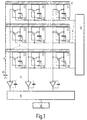
- FIG. 1 A sensor is provided for each pixel (pixel), which comprises a switching element 1, a capacitance 2 and a photosensor.
- the typically 2000 x 2000 switching elements are realized on a common dielectric substrate (glass) using thin-film technology (for example in the form of thin-film field-effect transistors 1, as indicated in FIG. 1).
- the photosensors are covered by a continuous photoconductor layer 3 covering the entire image field.
- a bias electrode 4 which is applied to the photoconductor layer and for each picture element a separate collecting electrode 11 is located on the other side of the photoconductor layer.
- the sensors are arranged in rows and columns in the manner of a matrix, the distance between the rows and the columns being the same. This distance determines the spatial resolution.
- the gate electrodes of the thin-film field effect transistors forming the switching elements are switched through line by line by means of a control circuit 6.
- the gate electrodes of all switching elements of a row are each connected to a common switching line 5.
- the source electrodes of the thin-film field effect transistors are each connected to the capacitance assigned to them, while their drain electrodes are connected in columns to a common output line 7.
- the ground line 10 and the switching lines 5 are applied to a substrate 15.
- the switching lines 5 are provided with vertical taps 17, which form the gate electrodes of the thin-film field-effect transistors.
- the electrode 11 thus has the function of the collecting and the source electrode, and in addition, together with a ground line 10 covered by it and a dielectric in between, it forms the storage capacitance 2.
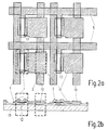
- the layers between the electrodes are very thin (in the order of magnitude of 0.2-1 ⁇ m). It is therefore important that the collecting electrodes 11 do not cover the switching lines 5, but in particular the output lines 7, because large parasitic capacitances would form between the collecting electrode 11 and the relevant electrodes. In the case of the output lines 7, this would lead to a capacitive signal decoupling and thus to a reduction in the readable signal and to increased noise of those connected to the output lines 7 Output amplifier 8 since they "see" a larger input capacitance.
- the collecting electrodes 11, on the one hand, and the lines 5, 7, on the other hand, must therefore be arranged next to one another, ie the top view of the collecting electrodes may, according to FIG. Fig. 2a do not overlap with lines 5 and 7. You must therefore restrict yourself to the area remaining between two adjacent switching lines 5 or two adjacent output lines 7.
- the collecting electrodes each comprise two electrode parts which are in electrical contact with one another, in that the first electrode part is arranged in a region next to the output line, in that the second electrode part has a larger area as the first electrode part and located between it and the bias electrode, and that there is an insulating layer between the second electrode part and the output line.
- the first electrode part forms a capacitance together with one of the reference or ground electrodes 10 and at the same time represents an electrode of the switching element, while the second electrode part generates those in the photoconductor layer Collects load carriers.
- the restrictions to which the first electrode part is subject do not apply to this second electrode part, ie the second electrode part can at least partially cover the lines, in particular the output lines, so that there is a comparatively high sensitivity.
- the parasitic capacitances resulting between this second electrode part and the lines can be kept small by making the insulating layer sufficiently thick.
- JP-OS 61-1177 or US Pat. No. 4,471,371 which relates to a thin-film image detector for visible light.
- Image detectors for visible light differ from X-ray image detectors in that instead of a relatively thick photoconductor layer they only have a thin semiconductor layer, for example made of amorphous silicon. This results in a relatively large capacity, so that a separate capacity - such as capacity 2 - is not required.
- the electrodes of the switching elements or the output line are located in a plane which is separated from the plane in which the collecting electrodes are located by an insulating layer produced using thin-film technology. This results in very high parasitic capacitances between the electrodes of the switching element and the collecting electrode, which cannot be tolerated in an X-ray image detector which is said to be readable with a high image frequency.
- a further development of the invention which is suitable for both solutions provides that layers are provided on both sides of the photoconductor layer with a small thickness compared to the photoconductor, which are doped in such a way that they provide one for the charge carriers which flow from the photoconductor to the electrodes adjacent to them have high conductivity compared to the conductivity for charge carriers with the opposite polarity.
- the two layers on both sides of the photoconductor layer block charge carriers injected from the collecting electrodes or from the biasing electrode, as a result of which the dark discharge rates are reduced.
- a layer is applied between the bias electrode and the layer adjacent to it, which layer consists of the same material as the photoconductor layer, but is considerably thinner than this. As a result, the dark discharge rates are once again significantly reduced.
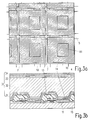
- an insulating layer 13 with a flat end surface is first applied to the thin-film structure shown in FIG. 2. In this end surface, contact holes are made above the collecting electrodes 11 by means of photolithographic processes, which reach as far as the electrodes 11.
- a metallic layer is then applied, for example by deposition from the vapor phase.
- This continuous layer of preferably aluminum is then structured by means of a photolithographic process in such a way that electrodes 14 which are as large as possible are formed for the individual pixels, which electrodes cover the area available for one pixel as completely as possible and which through the contact holes with the electrodes underneath 11 have electrical contact.
- the distance between the facing each other Edges of adjacent collecting electrodes can be between 5 and 15 ⁇ m, so that the ratio between the collecting electrode area and the area available for a pixel can still be up to 90% even with a pixel size of 100 ⁇ m.
- the electrodes 14 can thus capture a much larger part of the charge carriers generated in the photoconductor than the electrodes 11, so that there is an improved sensitivity.
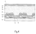
- the insulating layer 13 must have a thickness of at least 3 ⁇ m, preferably 5 to 10 ⁇ m. A relative dielectric constant of 4 to 5 is assumed (with a higher dielectric constant, the insulating layer must be even larger). Silicon oxide, silicon nitride or polyimide are suitable materials.
- the insulating layer is preferably applied in several individual layers, each with a smaller thickness. This is shown in FIG. 4, the insulating layer being formed by the sub-layers 131 and 132.
- the contact holes provided for the purpose of contacting the electrode parts 11 and 14 preferably have an increasing size, so that there are steps which ensure good metallization through the layer 14. It can be advantageous to use different materials for the different sublayers (for example, layer 131 can be made of silicon oxide and layer 132 can be made of polyimide). If etching agents are then used in the etching process required to produce the contact holes, each of which attacks only one of the partial layers, then it is easily possible to stop the etching process at a defined depth for the individual layers.
- the actual photoconductor layer 3 is then applied to the structure formed after the electrodes 14 have been applied.
- the photoconductor layer 3 is finally provided with a metallic cover electrode 4 made of gold or aluminum. It can prove advantageous to construct the photoconductor as a multilayer structure as follows:
- a semiconducting layer 31 is applied, which practically does not conduct negative charge carriers, but positive charge carriers all the better.
- This layer can consist of different materials, such as HgI 2 , CdSe, CdTe, PbO or Se, the conductivity of which is set by certain additives in the above sense. This is achieved, for example, with a 1-5 ⁇ m thick selenium layer doped with 20 to 200 ppm Cl.
- the actual photoconductor layer 32 made of amorphous selenium is then deposited with an addition of 0.1 to 1% arsenic. This layer must be between 200 and 800 ⁇ m thick in order to be able to sufficiently absorb the X-ray quanta that result from a medical examination.
- a semiconductor layer 33 is applied to the layer 32 and is doped in such a way that it does not conduct positive charge carriers, that is to say holes, but the better the negative charge carriers (electrons).
- This layer can consist, for example, of selenium which consists of 20 to 200 ppm alkali metal (Li, Na, K, Cs) and has a thickness between 0.5 and 2 ⁇ m.
- a positive voltage between 1 and 10 kV is applied to the bias electrode 4.
- the semiconductor layers 31 and 33 are then intended to block the charge carriers which may be injected from the collecting electrodes 14 or the top electrode 4, so that the dark discharge rates are decisively reduced.
- this function is only satisfactorily fulfilled if there is still a thin semiconducting layer between the doped layer 33 and the bias electrode 4 made of gold or aluminum, which is not very conductive for negative and positive charge carriers, for example a selenium layer, which coexists in the same way Arsenic is doped like the actual photoconductor layer 32.
- This means that the thickness of the layer 32 of 0.3 mm up to 5 kV are applied to the bias electrode without there being any significant dark currents (with a density of more than 1 pA / cm 2 ).
- An X-ray image is read out with such an X-ray image detector in a manner similar to that described in EP-OS 444 720.
- the switching elements 1 are closed (conductive) so that the capacitors 2 cannot charge.
- the X-ray exposure can be carried out with an image frequency of e.g. 60 frames / sec take place, the dose for the images should be between 10 nGy and 50 ⁇ Gy.
- Switches 1 are normally open during the X-ray exposure. To read out the x-ray image, all switching elements of a single line are closed simultaneously for a short time (10 to 20 ⁇ s) by applying a corresponding potential to the associated switching line 5. During this time, the charges collected from the capacitors 2 flow via the output lines 7 to the inputs of the amplifiers 8. The amplifiers are connected as current integrators, so that their output signal corresponds to the total charge that has flowed from the capacitor. The collecting electrodes 11, 14 are virtually kept at ground potential. The output signals of the amplifiers are taken over by an analog multiplexer 9, which deforms a serial signal stream with a correspondingly higher bandwidth from the parallel signals. The entire process is then repeated for the next and successively for all other image lines.
- the amplifiers 8 cannot currently be realized with the required sensitivity and low noise in thin-film technology. They must therefore be located outside the thin film substrate and implemented using conventional integrated circuit technology. Approx. 32 to 256 amplifiers with the associated analog multiplexer can be integrated on one chip. For a total of 2000 image columns, between 8 and 64 chips of this type would then be required, the inputs of which should be connected to the output lines located on the thin-film substrate would be. The outputs of the analog multiplexers are connected to analog-digital converters, after which the digital data are further processed.
- the insulating layer 13 is produced with a layer thickness customary for thin-layer technology (between 0.5 ⁇ m and a maximum of 2 ⁇ m), a contact hole extending up to the collecting electrode 11 being provided above each of the collecting electrodes.
- Analog structures can also be realized in other semiconductor materials such as HgI 2 , CdTe, CDSe or PbO.
- a negative voltage is applied to the bias electrode, so that negative charge carriers (electrons) migrate to the collecting electrode during X-ray exposure, the layers with good conductivity for positive charge carriers (holes) and poor conductivity for electrons are closed swap and vice versa.
- a semiconducting layer 35 is applied to the insulating layer 13, which does not conduct the negative charge carriers, but has a good conductivity for positive charge carriers.
- it is a selenium layer which - like layer 31 - is doped with 20 to 200 ppm CI, but which is thicker than layer 31 of FIG. 3, for example 5 to 40 ⁇ m.
- FIG. 6 corresponds to FIG. 5b, but the electrical field lines or the paths of the electrical charge carriers are shown.
- a positive voltage of, for example, 3 kV is applied to the bias electrode 4 and charge carriers are generated in the photoconductor layer 32, here for example selenium doped with 0.1 to 1% arsenic, by X-ray exposure, positive space charges form above the areas passivated by the insulating layer 13. As a result, the electric field is deformed, as indicated in FIG. 6. Because of the good conductivity of layer 35 for holes, even charge carriers that were not generated above the collecting electrode can now reach the collecting electrode at high speed in this layer. Possibly. Electrons injected from the collecting electrodes 11 are held in the layer 35; at this point the layer acts analogously to layer 31 in FIGS. 3 and 4.
- the good conductivity of layer 35 for positive charge carriers at the same time means that the space charge in this layer can easily flow apart, as is outlined in FIG. 6.
- the desired field distortion will be relatively low in the state of equilibrium.
- the field distortion can extend into the actual photoconductor layer 32.
- this has a low conductivity for the positive charge carriers, which inhibits the transport to the collecting electrode.
- FIG. 7 A further development of this detector is shown in Figure 7.
- a further semiconductor layer 36 is inserted under the layer which is good for holes and poorly for electrons and which has approximately equally low conductivity for both polarities of charge carriers.
- this layer is approximately 1-40 ⁇ m thick and consists of selenium, doped with 0.1 to 1% arsenic. Because of its lower conductivity for positive charge carriers, the space charge builds up more efficiently because it cannot flow apart parallel to the substrate. The field bending is thus forced and to a large extent localized in the layer 35, which is highly conductive for holes. The transfer of the charge carriers to the collecting electrode, which now takes place predominantly in the layer 35 which is conductive for holes, is thus made possible in such a way that a maximum signal is obtained in a short time.
- electrons injected from the collecting electrodes are held in the layer 35. The fact that they have previously passed through layer 36 is irrelevant to the functionality of the detector.
- the collecting electrodes can each comprise an additional electrode part 16, which - as shown in FIG. 8 - covers the associated thin film transistor above the insulating layer 13 and which is in electrical contact with the electrode part 11.
- These electrode parts are produced by metallizing the surface, which arises after the application of the insulating layer and the application of the contact holes but before the application of the semiconducting layer 35.
Landscapes
- General Physics & Mathematics (AREA)
- Engineering & Computer Science (AREA)
- Signal Processing (AREA)
- Physics & Mathematics (AREA)
- Health & Medical Sciences (AREA)
- Life Sciences & Earth Sciences (AREA)
- Molecular Biology (AREA)
- High Energy & Nuclear Physics (AREA)
- Multimedia (AREA)
- Spectroscopy & Molecular Physics (AREA)
- Measurement Of Radiation (AREA)
- Solid State Image Pick-Up Elements (AREA)
- Light Receiving Elements (AREA)
- Conversion Of X-Rays Into Visible Images (AREA)
Claims (9)
- Détecteur d'images radiologiques avec plusieurs capteurs sensibles aux rayons X présentant les caractéristiques suivantes :- chaque détecteur contient une électrode collectrice (11) et un élément de circuit (1) qui relie l'électrode collectrice à une ligne de sortie (7);- entre les électrodes collectrices individuelles (11) et une électrode de polarisation (4) se trouve une couche photoconductrice (3);- les électrodes collectrices forment avec les électrodes de référence (10) des capacités (2) qui peuvent être chargées par les porteurs de charge générés par le photoconducteur,caractérisé en ce que les électrodes collectrices comprennent respectivement deux parties d'électrode (11, 14) en contact électrique l'une avec l'autre, que la première partie d'électrode (11) est respectivement disposée dans une zone adjacente à la ligne de sortie correspondante (7), que la deuxième partie d'électrode (14) présente une surface plus grande que la première partie d'électrode et se situe entre celle-ci et l'électrode de polarisation et qu'une couche d'isolation se trouve entre la deuxième partie de l'électrode (14) et la ligne de sortie (7).
- Détecteur d'images radiologiques avec plusieurs détecteurs sensibles aux rayons X présentant les caractéristiques suivantes :- chaque capteur contient une électrode collectrice (11) et un élément de circuit (1) qui relie l'électrode collectrice à une ligne de sortie (7);- entre les électrodes collectrices individuelles (11) et une électrode de polarisation (4) se trouve une couche photoconductrice (3);- les électrodes collectrices forment avec les électrodes de référence (10) des capacités (2) qui peuvent être chargées par des porteurs de charge générés dans le photoconducteur,caractérisé par les caractéristiques suivantes :- l'électrode collectrice (11) est disposée dans la région adjacente à la ligne de sortie (7);- l'élément de circuit (1) et la ligne de sortie sont recouverts par une couche d'isolation (13);- la couche d'isolation (13) et l'électrode collectrice (11) sont recouvertes par une couche semi-conductrice (35);- la couche semi-conductrice (35) est dotée de telle sorte qu'elle présente une grande conductibilité pour les porteurs de charge circulant dans la direction de l'électrode collectrice par rapport à la conductibilité pour les porteurs de charge de polarité opposée.
- Détecteur d'images radiologiques selon la revendication 2,
caractérisé en ce qu'une couche semi-conductrice (36) supplémentaire se trouve entre la couche semi-conductrice (35) et les électrodes collectrices (11) et présente une faible conductibilité à la fois pour les porteurs de charge positifs et négatifs. - Détecteur d'images radiologiques selon la revendication 2,
caractérisé en ce que les électrodes collectrices (11, 16) se composent respectivement de deux parties d'électrode qui sont en contact électrique l'une avec l'autre, que la première partie d'électrode est disposée dans la région adjacente à la ligne de sortie et que la deuxième électrode (16) se trouve sur la couche d'isolation au-dessus de l'élément de circuit correspondant (1) et est recouverte pour sa part par la couche semi-conductrice (35). - Détecteur d'images radiologiques selon l'une des revendications précédentes,
caractérisé en ce que la couche photoconductrice (32) se compose essentiellement de sélénium. - Détecteur d'images radiologiques selon l'une des revendications 1 à 4,
caractérisé en ce que la couche photoconductrice se compose essentiellement d'une des matières suivantes : PbO, CdTe, CdSe ou HgI2. - Détecteur d'images radiologiques selon l'une des revendications précédentes,
caractérisé en ce que, de part et d'autre de la couche photoconductrice (32), sont prévues des couches (31, 33) avec une épaisseur minime par rapport à la couche photoconductrice (32) qui sont dotées de telle sorte qu'elles présentent pour les porteurs de charge qui circulent de la couche photoconductrice vers les électrodes voisines (11; 4) une grande conductibilité par rapport à la conductibilité pour les porteurs de charge de polarité opposée. - Détecteur d'images radiologiques selon la revendication 7,
caractérisé en ce qu'une couche supplémentaire (34) qui se compose du même matériau que la couche photoconductrice mais est essentiellement plus fine que celle-ci est disposée entre l'électrode de polarisation (4) et la couche semi-conductrice (35) voisine de celle-ci. - Détecteur d'images radiologiques selon la revendication 1,
caractérisé en ce que la couche d'isolation (13) est formée de plusieurs couches partielles (131, 132) qui se recouvrent mutuellement en matériaux différents et que les ouvertures dans les couches d'isolation par lesquelles les deux parties d'électrode (11,14) sont en contact l'une avec l'autre sont d'autant plus grandes que la couche partielle est éloignée de la première partie d'électrode (11).
Applications Claiming Priority (2)
| Application Number | Priority Date | Filing Date | Title |
|---|---|---|---|
| DE4227096A DE4227096A1 (de) | 1992-08-17 | 1992-08-17 | Röntgenbilddetektor |
| DE4227096 | 1992-08-17 |
Publications (3)
| Publication Number | Publication Date |
|---|---|
| EP0588397A2 EP0588397A2 (fr) | 1994-03-23 |
| EP0588397A3 EP0588397A3 (fr) | 1994-05-04 |
| EP0588397B1 true EP0588397B1 (fr) | 1997-06-04 |
Family
ID=6465667
Family Applications (1)
| Application Number | Title | Priority Date | Filing Date |
|---|---|---|---|
| EP93202357A Expired - Lifetime EP0588397B1 (fr) | 1992-08-17 | 1993-08-11 | Détecteur d'images radiologiques |
Country Status (4)
| Country | Link |
|---|---|
| US (1) | US5396072A (fr) |
| EP (1) | EP0588397B1 (fr) |
| JP (1) | JPH06209097A (fr) |
| DE (2) | DE4227096A1 (fr) |
Families Citing this family (97)
| Publication number | Priority date | Publication date | Assignee | Title |
|---|---|---|---|---|
| GB9414639D0 (en) * | 1994-07-20 | 1994-09-07 | Philips Electronics Uk Ltd | An image detector |
| DE4426451C2 (de) * | 1994-07-26 | 1998-07-16 | Siemens Ag | Röntgendiagnostikeinrichtungen mit einem Festkörperbildwandler |
| US5869837A (en) * | 1994-07-27 | 1999-02-09 | Litton Systems Canada Limited | Radiation imaging panel |
| US5498880A (en) * | 1995-01-12 | 1996-03-12 | E. I. Du Pont De Nemours And Company | Image capture panel using a solid state device |
| WO1996034416A1 (fr) * | 1995-04-28 | 1996-10-31 | Sunnybrook Hospital | Dispositif d'imagerie par rayons-x a matrice active |
| US5641974A (en) * | 1995-06-06 | 1997-06-24 | Ois Optical Imaging Systems, Inc. | LCD with bus lines overlapped by pixel electrodes and photo-imageable insulating layer therebetween |
| US6124606A (en) * | 1995-06-06 | 2000-09-26 | Ois Optical Imaging Systems, Inc. | Method of making a large area imager with improved signal-to-noise ratio |
| US5648674A (en) * | 1995-06-07 | 1997-07-15 | Xerox Corporation | Array circuitry with conductive lines, contact leads, and storage capacitor electrode all formed in layer that includes highly conductive metal |
| US5619033A (en) * | 1995-06-07 | 1997-04-08 | Xerox Corporation | Layered solid state photodiode sensor array |
| EP0842541B1 (fr) | 1995-07-31 | 2002-02-13 | iFire Technology Inc. | Detecteur de panneau de radiographie a charges-pieges reduites |
| JP2001509252A (ja) * | 1995-07-31 | 2001-07-10 | リットン システムズ カナダ リミテッド | 電子ノイズの少ない放射線画像形成のためのフラットパネル検出器 |
| WO1997005657A1 (fr) * | 1995-07-31 | 1997-02-13 | Litton Systems Canada Limited | Technique et appareil de commande d'un imageur a rayonnement electromagnetique tft double grille |
| US6232606B1 (en) | 1995-07-31 | 2001-05-15 | Ifire Technology, Inc. | Flat panel detector for radiation imaging and pixel for use therein |
| EP0791230B1 (fr) * | 1995-09-12 | 2008-08-13 | Koninklijke Philips Electronics N.V. | Capteur d'images radiographiques |
| GB9520791D0 (en) * | 1995-10-13 | 1995-12-13 | Philips Electronics Nv | Image sensor |
| US5733804A (en) * | 1995-12-22 | 1998-03-31 | Xerox Corporation | Fabricating fully self-aligned amorphous silicon device |
| US5717223A (en) * | 1995-12-22 | 1998-02-10 | Xerox Corporation | Array with amorphous silicon TFTs in which channel leads overlap insulating region no more than maximum overlap |
| US5652430A (en) * | 1996-05-03 | 1997-07-29 | Sterling Diagnostic Imaging, Inc. | Direct radiographic imaging panel |
| EP0897597B1 (fr) | 1996-05-08 | 2002-09-11 | iFire Technology Inc. | Panneau plat a haute resolution pour imagerie radiologique |
| US5770871A (en) * | 1996-06-20 | 1998-06-23 | Xerox Corporation | Sensor array with anticoupling layer between data lines and charge collection electrodes |
| CA2184667C (fr) * | 1996-09-03 | 2000-06-20 | Bradley Trent Polischuk | Plaque multicouche pour la radiographie et methode de fabrication de cette plaque |
| DE19640946A1 (de) * | 1996-10-04 | 1998-04-16 | Philips Patentverwaltung | Röntgenaufnahme-Anordnung mit einem Photoleiter |
| DE69731600D1 (de) | 1996-12-20 | 2004-12-23 | Canon Kk | Bildaufnahmevorrichtung,-verfahren und -system |
| WO1998044568A2 (fr) * | 1997-04-02 | 1998-10-08 | Koninklijke Philips Electronics N.V. | Appareil de radiographie a capteur matriciel |
| JP2000512084A (ja) * | 1997-04-02 | 2000-09-12 | コーニンクレッカ フィリップス エレクトロニクス エヌ ヴィ | センサマトリックスを有するx線装置 |
| WO1998048599A2 (fr) * | 1997-04-24 | 1998-10-29 | Koninklijke Philips Electronics N.V. | Commande d'exposition sur la base d'une partie correspondante de radiographie |
| US5895936A (en) * | 1997-07-09 | 1999-04-20 | Direct Radiography Co. | Image capture device using a secondary electrode |
| JP3413084B2 (ja) | 1997-11-20 | 2003-06-03 | キヤノン株式会社 | 放射線撮像装置及び撮像方法 |
| IL123006A (en) | 1998-01-20 | 2005-12-18 | Edge Medical Devices Ltd | X-ray imaging system |
| US5994157A (en) * | 1998-01-22 | 1999-11-30 | Ois Optical Imaging Systems, Inc. | Method of making a large area imager with UV Blocking layer, and corresponding imager |
| US6020590A (en) * | 1998-01-22 | 2000-02-01 | Ois Optical Imaging Systems, Inc. | Large area imager with UV blocking layer |
| US6060714A (en) * | 1998-01-23 | 2000-05-09 | Ois Optical Imaging Systems, Inc. | Large area imager with photo-imageable interface barrier layer |
| US6229192B1 (en) | 1998-01-27 | 2001-05-08 | Ois Optical Imaging Systems, Inc. | Image sensor or LCD including switching pin diodes |
| US6180529B1 (en) | 1998-01-27 | 2001-01-30 | Ois Optical Imaging Systems, Inc. | Method of making an image sensor or LCD including switching pin diodes |
| US6410921B1 (en) * | 1998-01-30 | 2002-06-25 | Konica Corporation | X-ray image recording system and x-ray image recording method |
| US5917199A (en) | 1998-05-15 | 1999-06-29 | Ois Optical Imaging Systems, Inc. | Solid state imager including TFTS with variably doped contact layer system for reducing TFT leakage current and increasing mobility and method of making same |
| CA2241779C (fr) | 1998-06-26 | 2010-02-09 | Ftni Inc. | Detecteur d'image radiologique indirecte pour utilisation avec la radiologie |
| CA2242743C (fr) | 1998-07-08 | 2002-12-17 | Ftni Inc. | Detecteur de rayons x a conversion photovoltaique dote de protection inherente contre la surtension, pour imagerie statique et dynamique |
| IL126018A0 (en) | 1998-09-01 | 1999-05-09 | Edge Medical Devices Ltd | X-ray imaging system |
| US20020092987A1 (en) * | 1998-09-05 | 2002-07-18 | Taehee Cho | Photo detect device using quantum dots and materialization method thereof |
| WO2000025151A1 (fr) | 1998-10-28 | 2000-05-04 | Koninklijke Philips Electronics N.V. | Procede de fabrication d'un detecteur a scintillation a couche |
| US6486470B2 (en) | 1998-11-02 | 2002-11-26 | 1294339 Ontario, Inc. | Compensation circuit for use in a high resolution amplified flat panel for radiation imaging |
| JP4059463B2 (ja) | 1998-12-10 | 2008-03-12 | 株式会社島津製作所 | 放射線検出装置 |
| US6326625B1 (en) | 1999-01-20 | 2001-12-04 | Edge Medical Devices Ltd. | X-ray imaging system |
| AU3853300A (en) * | 1999-03-15 | 2000-10-04 | Mamea Imaging Ab | Device and method relating to x-ray imaging |
| KR100443902B1 (ko) * | 1999-03-25 | 2004-08-09 | 엘지.필립스 엘시디 주식회사 | 엑스레이 영상 감지소자 및 그 제조방법 |
| JP3838806B2 (ja) * | 1999-03-26 | 2006-10-25 | 株式会社東芝 | 信号増倍x線撮像装置 |
| US8120683B1 (en) * | 1999-04-08 | 2012-02-21 | Nova R & D, Inc. | High resoultion digital imaging apparatus |
| WO2000068710A2 (fr) | 1999-05-10 | 2000-11-16 | Lippens Francois | Systemes de detection selective d'energie |
| US6178225B1 (en) | 1999-06-04 | 2001-01-23 | Edge Medical Devices Ltd. | System and method for management of X-ray imaging facilities |
| DE19926582A1 (de) * | 1999-06-11 | 2000-12-14 | Philips Corp Intellectual Pty | Sensor |
| US20020121605A1 (en) * | 1999-06-17 | 2002-09-05 | Lutz Fink | Semiconductor sensor and method for its wiring |
| DE19927694C1 (de) * | 1999-06-17 | 2000-11-02 | Lutz Fink | Halbleitersensor mit einer Pixelstruktur |
| US6281507B1 (en) | 1999-06-30 | 2001-08-28 | Siemens Medical Systems, Inc. | Interdigital photoconductor structure for direct X-ray detection in a radiography imaging system |
| JP3832615B2 (ja) * | 1999-08-26 | 2006-10-11 | 株式会社島津製作所 | 放射線検出装置 |
| US6510202B2 (en) | 2000-03-31 | 2003-01-21 | Canon Kabushiki Kaisha | Imaging apparatus, imaging method, and storage medium |
| JP4557357B2 (ja) * | 2000-03-31 | 2010-10-06 | キヤノン株式会社 | 撮影制御装置、撮影制御方法及び記憶媒体 |
| JP4731698B2 (ja) | 2000-04-06 | 2011-07-27 | キヤノン株式会社 | 画像処理装置、撮影装置、画像処理システム、画像処理方法、及び記憶媒体 |
| JP3708440B2 (ja) * | 2001-01-30 | 2005-10-19 | シャープ株式会社 | イメージセンサ |
| DE10131420C2 (de) * | 2001-06-29 | 2003-07-10 | Lutz Fink | Halbleitersensor sowie Beschaltungsverfahren dafür |
| CN1316634C (zh) * | 2001-10-03 | 2007-05-16 | 株式会社东芝 | X光平面检测器 |
| CA2363663C (fr) * | 2001-11-22 | 2004-10-19 | Ftni Inc. | Detecteur a rayons x a ecran plat et a conversion directe avec suppression automatique des images fantomes |
| US6730900B2 (en) * | 2002-02-05 | 2004-05-04 | E-Phocus, Inc. | Camera with MOS or CMOS sensor array |
| JP4188619B2 (ja) * | 2002-04-23 | 2008-11-26 | 株式会社島津製作所 | X線検出器 |
| US7214945B2 (en) | 2002-06-11 | 2007-05-08 | Canon Kabushiki Kaisha | Radiation detecting apparatus, manufacturing method therefor, and radiation image pickup system |
| JP4269653B2 (ja) * | 2002-11-20 | 2009-05-27 | 株式会社島津製作所 | 放射線検出器の製造方法 |
| WO2004095580A1 (fr) * | 2003-04-24 | 2004-11-04 | Philips Intellectual Property & Standards Gmbh | Element detecteur pour rayons x |
| JP2005012049A (ja) * | 2003-06-20 | 2005-01-13 | Shimadzu Corp | 放射線検出器およびそれを備えた放射線撮像装置 |
| JP2005019543A (ja) * | 2003-06-24 | 2005-01-20 | Shimadzu Corp | 二次元半導体検出器および二次元撮像装置 |
| JP4468083B2 (ja) * | 2003-08-26 | 2010-05-26 | キヤノン株式会社 | 放射線撮影装置、放射線撮影方法 |
| US20050056829A1 (en) * | 2003-09-17 | 2005-03-17 | Green Michael C. | Reducing dark current of photoconductor using heterojunction that maintains high x-ray sensitivity |
| JP2005101193A (ja) * | 2003-09-24 | 2005-04-14 | Shimadzu Corp | 放射線検出器 |
| US7304308B2 (en) * | 2005-02-16 | 2007-12-04 | Hologic, Inc. | Amorphous selenium flat panel x-ray imager for tomosynthesis and static imaging |
| US7233005B2 (en) * | 2005-02-16 | 2007-06-19 | Hologic, Inc. | Amorphous selenium flat panel x-ray imager for tomosynthesis and static imaging |
| US7122803B2 (en) * | 2005-02-16 | 2006-10-17 | Hologic, Inc. | Amorphous selenium flat panel x-ray imager for tomosynthesis and static imaging |
| JP2005260263A (ja) * | 2005-04-18 | 2005-09-22 | Toshiba Corp | X線撮像装置 |
| DE102005037290A1 (de) * | 2005-08-08 | 2007-02-22 | Siemens Ag | Flachbilddetektor |
| EP1780802B1 (fr) | 2005-11-01 | 2012-03-28 | Fujifilm Corporation | Détecteur d'images à rayons X à base de sélénium amorphe |
| JP2008078597A (ja) * | 2005-11-01 | 2008-04-03 | Fujifilm Corp | 放射線画像検出器 |
| US7723692B2 (en) * | 2005-11-21 | 2010-05-25 | Fujifilm Corporation | Solid state radiation sensor and manufacturing method of the same |
| JP4861789B2 (ja) * | 2006-10-18 | 2012-01-25 | サニーブルック・ホスピタル | アクティブマトリックスx線撮像アレイ |
| JP2008210906A (ja) * | 2007-02-26 | 2008-09-11 | Fujifilm Corp | 放射線画像検出器 |
| US8232531B2 (en) * | 2007-03-29 | 2012-07-31 | Varian Medical Systems, Inc. | Corrosion barrier layer for photoconductive X-ray imagers |
| KR101218089B1 (ko) * | 2007-12-07 | 2013-01-18 | 엘지디스플레이 주식회사 | 디지털 엑스레이 디텍터 및 그 제조방법 |
| JP5070130B2 (ja) * | 2008-05-26 | 2012-11-07 | 富士フイルム株式会社 | 放射線検出器 |
| JP5233521B2 (ja) * | 2008-08-29 | 2013-07-10 | 大日本印刷株式会社 | Icチップ、データ読出し方法、データ読出しプログラム及び記録媒体等 |
| KR101217809B1 (ko) * | 2011-07-06 | 2013-01-21 | 주식회사 디알텍 | 광 스위칭을 이용한 엑스레이 디텍터 |
| US9261609B2 (en) * | 2012-08-20 | 2016-02-16 | General Electric Company | Apparatus and methods for charge collection control in radiation detectors |
| JP6105903B2 (ja) | 2012-11-09 | 2017-03-29 | キヤノン株式会社 | 画像処理装置、画像処理方法、放射線撮影システム及びプログラム |
| JP2014110353A (ja) * | 2012-12-03 | 2014-06-12 | Canon Inc | 検出装置及び放射線検出システム |
| BR112015012775A2 (pt) * | 2012-12-04 | 2017-07-11 | Koninklijke Philips Nv | unidade de detector de raios x de contagem de fótons; detector de raios x de contagem de fótons; e método de detecção de raios x de contagem de fótons |
| US9364191B2 (en) | 2013-02-11 | 2016-06-14 | University Of Rochester | Method and apparatus of spectral differential phase-contrast cone-beam CT and hybrid cone-beam CT |
| JP5424371B1 (ja) | 2013-05-08 | 2014-02-26 | 誠 雫石 | 固体撮像素子及び撮像装置 |
| DE102014201772B4 (de) * | 2014-01-31 | 2017-10-12 | Siemens Healthcare Gmbh | Direktkonvertierender Röntgenstrahlungsdetektor, CT-System und Verfahren hierzu |
| WO2017136925A1 (fr) * | 2016-02-08 | 2017-08-17 | Thunder Bay Regional Health Research Institute | Dispositifs de détection d'énergie à base d'oxyde de plomb amorphe, et leurs procédés de fabrication |
| WO2017171414A1 (fr) * | 2016-03-31 | 2017-10-05 | Vieworks Co., Ltd. | Détecteur d'imagerie par rayonnement à gain de charge proportionnel pendant la lecture |
| EP3428691A1 (fr) | 2017-07-13 | 2019-01-16 | Koninklijke Philips N.V. | Détecteur de rayons x et son procédé de fabrication |
Family Cites Families (9)
| Publication number | Priority date | Publication date | Assignee | Title |
|---|---|---|---|---|
| US4233514A (en) * | 1978-12-14 | 1980-11-11 | General Electric Company | Solid state radiation detector and arrays thereof |
| US4471371A (en) * | 1981-01-06 | 1984-09-11 | Fuji Xerox Co., Ltd. | Thin film image pickup element |
| JPS611177A (ja) * | 1985-05-24 | 1986-01-07 | Hitachi Ltd | 固体撮像素子 |
| FR2623019B1 (fr) * | 1987-11-10 | 1990-05-11 | Thomson Csf | Dispositif de prise d'image radiologique |
| JPH03150876A (ja) * | 1989-11-08 | 1991-06-27 | Fujitsu Ltd | フォト・ダイオード |
| US5117114A (en) * | 1989-12-11 | 1992-05-26 | The Regents Of The University Of California | High resolution amorphous silicon radiation detectors |
| DE4002429A1 (de) * | 1990-01-27 | 1991-08-01 | Philips Patentverwaltung | Sensormatrix |
| US5166524A (en) * | 1991-06-28 | 1992-11-24 | E. I. Du Pont De Nemours & Company | Element, device and associated method for capturing a latent radiographic image |
| US5168160A (en) * | 1991-06-28 | 1992-12-01 | E. I. Du Pont De Nemours And Company | Method and apparatus for acquiring an electrical signal representing a radiographic image |
-
1992
- 1992-08-17 DE DE4227096A patent/DE4227096A1/de not_active Withdrawn
-
1993
- 1993-08-11 EP EP93202357A patent/EP0588397B1/fr not_active Expired - Lifetime
- 1993-08-11 DE DE59306646T patent/DE59306646D1/de not_active Expired - Fee Related
- 1993-08-13 JP JP5201719A patent/JPH06209097A/ja active Pending
- 1993-08-17 US US08/107,548 patent/US5396072A/en not_active Expired - Lifetime
Also Published As
| Publication number | Publication date |
|---|---|
| DE59306646D1 (de) | 1997-07-10 |
| JPH06209097A (ja) | 1994-07-26 |
| DE4227096A1 (de) | 1994-02-24 |
| EP0588397A2 (fr) | 1994-03-23 |
| EP0588397A3 (fr) | 1994-05-04 |
| US5396072A (en) | 1995-03-07 |
Similar Documents
| Publication | Publication Date | Title |
|---|---|---|
| EP0588397B1 (fr) | Détecteur d'images radiologiques | |
| DE69526457T2 (de) | Bilddetektor | |
| DE69623659T2 (de) | Hochauflösender flacher sensor für strahlungsabbildungssystem | |
| DE69327898T2 (de) | Elektronisches Verfahren und Vorrichtung zur Erfassung eines Röntgenstrahlungsbildes | |
| DE69317230T2 (de) | Methode und Apparat zur Gerinnung eines Röntgenbildes unter Verwendung eines Festkörper-Elementes | |
| DE69510826T2 (de) | Flache abbildungsvorrichtung | |
| EP0440282B1 (fr) | Matrice de détecteurs | |
| DE69635303T2 (de) | Röntgenstrahlungs-bildsensor | |
| DE69637176T2 (de) | Flache Bildaufnahmevorrichtung mit planarer Masseelektrode | |
| DE69636944T2 (de) | Festkörperbildaufnahmeanordnung mit Abschirmungsleitern in der Gatelektrodenebene | |
| DE69636471T2 (de) | Flache Bildaufnahmevorrichtung mit gemeinsamer gemusterter Elektrode | |
| DE4002429A1 (de) | Sensormatrix | |
| DE69033565T2 (de) | Bildfächensensor vom Interline-Transfer-Typ mit einer Elektrodenstruktur für jeden Pixel | |
| DE69526676T2 (de) | Fluessigkristall-anzeigevorrichtung mit pixeln von hoher kapazitaet | |
| DE69525477T2 (de) | Flacher detektor für strahlungsabbildung mit reduzierten gespeicherten ladungen | |
| DE69417407T2 (de) | Geräuscharme fluoroskopische festkörperbildaufnahmevorrichtung für strahlung | |
| DE2623541B2 (de) | Bildaufnahmeanordnung und photoempfindliches Element für eine solche Anordnung | |
| DE60033894T2 (de) | Strahlungsdetektor | |
| EP0007384B1 (fr) | Détecteur de transfert de charge unidimensionnel avec dispositif de débordement | |
| DE10315036B4 (de) | Bildgebungsanordnung | |
| DE4422928A1 (de) | Zweidimensionaler Strahlungsdetektor | |
| DE3529025C2 (fr) | ||
| DE69030381T2 (de) | Spektrometer mit ladungsdetektor | |
| DE3733114A1 (de) | Strahlungsdetektor | |
| DE69025173T2 (de) | Festkörper-bildsensor |
Legal Events
| Date | Code | Title | Description |
|---|---|---|---|
| PUAI | Public reference made under article 153(3) epc to a published international application that has entered the european phase |
Free format text: ORIGINAL CODE: 0009012 |
|
| PUAL | Search report despatched |
Free format text: ORIGINAL CODE: 0009013 |
|
| AK | Designated contracting states |
Kind code of ref document: A2 Designated state(s): DE FR GB IT NL |
|
| AK | Designated contracting states |
Kind code of ref document: A3 Designated state(s): DE FR GB IT NL |
|
| RAP1 | Party data changed (applicant data changed or rights of an application transferred) |
Owner name: N.V. PHILIPS' GLOEILAMPENFABRIEKEN Owner name: PHILIPS PATENTVERWALTUNG GMBH |
|
| 17P | Request for examination filed |
Effective date: 19941019 |
|
| 17Q | First examination report despatched |
Effective date: 19950503 |
|
| GRAG | Despatch of communication of intention to grant |
Free format text: ORIGINAL CODE: EPIDOS AGRA |
|
| GRAH | Despatch of communication of intention to grant a patent |
Free format text: ORIGINAL CODE: EPIDOS IGRA |
|
| GRAH | Despatch of communication of intention to grant a patent |
Free format text: ORIGINAL CODE: EPIDOS IGRA |
|
| GRAA | (expected) grant |
Free format text: ORIGINAL CODE: 0009210 |
|
| AK | Designated contracting states |
Kind code of ref document: B1 Designated state(s): DE FR GB IT NL |
|
| PG25 | Lapsed in a contracting state [announced via postgrant information from national office to epo] |
Ref country code: NL Free format text: LAPSE BECAUSE OF FAILURE TO SUBMIT A TRANSLATION OF THE DESCRIPTION OR TO PAY THE FEE WITHIN THE PRESCRIBED TIME-LIMIT Effective date: 19970604 Ref country code: IT Free format text: LAPSE BECAUSE OF FAILURE TO SUBMIT A TRANSLATION OF THE DESCRIPTION OR TO PAY THE FEE WITHIN THE PRESCRIBED TIME-LIMIT;WARNING: LAPSES OF ITALIAN PATENTS WITH EFFECTIVE DATE BEFORE 2007 MAY HAVE OCCURRED AT ANY TIME BEFORE 2007. THE CORRECT EFFECTIVE DATE MAY BE DIFFERENT FROM THE ONE RECORDED. Effective date: 19970604 |
|
| REF | Corresponds to: |
Ref document number: 59306646 Country of ref document: DE Date of ref document: 19970710 |
|
| GBT | Gb: translation of ep patent filed (gb section 77(6)(a)/1977) |
Effective date: 19970728 |
|
| ET | Fr: translation filed | ||
| NLV1 | Nl: lapsed or annulled due to failure to fulfill the requirements of art. 29p and 29m of the patents act | ||
| PLBE | No opposition filed within time limit |
Free format text: ORIGINAL CODE: 0009261 |
|
| 26N | No opposition filed | ||
| REG | Reference to a national code |
Ref country code: FR Ref legal event code: CD |
|
| REG | Reference to a national code |
Ref country code: GB Ref legal event code: IF02 |
|
| REG | Reference to a national code |
Ref country code: GB Ref legal event code: 746 Effective date: 20050518 |
|
| REG | Reference to a national code |
Ref country code: FR Ref legal event code: D6 |
|
| PGFP | Annual fee paid to national office [announced via postgrant information from national office to epo] |
Ref country code: GB Payment date: 20050830 Year of fee payment: 13 |
|
| GBPC | Gb: european patent ceased through non-payment of renewal fee |
Effective date: 20060811 |
|
| PG25 | Lapsed in a contracting state [announced via postgrant information from national office to epo] |
Ref country code: GB Free format text: LAPSE BECAUSE OF NON-PAYMENT OF DUE FEES Effective date: 20060811 |
|
| PGFP | Annual fee paid to national office [announced via postgrant information from national office to epo] |
Ref country code: FR Payment date: 20080827 Year of fee payment: 16 |
|
| PGFP | Annual fee paid to national office [announced via postgrant information from national office to epo] |
Ref country code: DE Payment date: 20081017 Year of fee payment: 16 |
|
| REG | Reference to a national code |
Ref country code: FR Ref legal event code: ST Effective date: 20100430 |
|
| PG25 | Lapsed in a contracting state [announced via postgrant information from national office to epo] |
Ref country code: FR Free format text: LAPSE BECAUSE OF NON-PAYMENT OF DUE FEES Effective date: 20090831 Ref country code: DE Free format text: LAPSE BECAUSE OF NON-PAYMENT OF DUE FEES Effective date: 20100302 |