EP0588397B1 - X-ray image detector - Google Patents
X-ray image detector Download PDFInfo
- Publication number
- EP0588397B1 EP0588397B1 EP93202357A EP93202357A EP0588397B1 EP 0588397 B1 EP0588397 B1 EP 0588397B1 EP 93202357 A EP93202357 A EP 93202357A EP 93202357 A EP93202357 A EP 93202357A EP 0588397 B1 EP0588397 B1 EP 0588397B1
- Authority
- EP
- European Patent Office
- Prior art keywords
- electrode
- layer
- collecting
- image detector
- ray image
- Prior art date
- Legal status (The legal status is an assumption and is not a legal conclusion. Google has not performed a legal analysis and makes no representation as to the accuracy of the status listed.)
- Expired - Lifetime
Links
Images

Classifications
-
- G—PHYSICS
- G01—MEASURING; TESTING
- G01T—MEASUREMENT OF NUCLEAR OR X-RADIATION
- G01T1/00—Measuring X-radiation, gamma radiation, corpuscular radiation, or cosmic radiation
- G01T1/16—Measuring radiation intensity
- G01T1/24—Measuring radiation intensity with semiconductor detectors
- G01T1/241—Electrode arrangements, e.g. continuous or parallel strips or the like
-
- H—ELECTRICITY
- H04—ELECTRIC COMMUNICATION TECHNIQUE
- H04N—PICTORIAL COMMUNICATION, e.g. TELEVISION
- H04N25/00—Circuitry of solid-state image sensors [SSIS]; Control thereof
- H04N25/70—SSIS architectures; Circuits associated therewith
- H04N25/76—Addressed sensors, e.g. MOS or CMOS sensors
-
- H—ELECTRICITY
- H10—SEMICONDUCTOR DEVICES; ELECTRIC SOLID-STATE DEVICES NOT OTHERWISE PROVIDED FOR
- H10F—INORGANIC SEMICONDUCTOR DEVICES SENSITIVE TO INFRARED RADIATION, LIGHT, ELECTROMAGNETIC RADIATION OF SHORTER WAVELENGTH OR CORPUSCULAR RADIATION
- H10F39/00—Integrated devices, or assemblies of multiple devices, comprising at least one element covered by group H10F30/00, e.g. radiation detectors comprising photodiode arrays
- H10F39/10—Integrated devices
- H10F39/12—Image sensors
- H10F39/18—Complementary metal-oxide-semiconductor [CMOS] image sensors; Photodiode array image sensors
- H10F39/189—X-ray, gamma-ray or corpuscular radiation imagers
- H10F39/1892—Direct radiation image sensors
-
- H—ELECTRICITY
- H10—SEMICONDUCTOR DEVICES; ELECTRIC SOLID-STATE DEVICES NOT OTHERWISE PROVIDED FOR
- H10F—INORGANIC SEMICONDUCTOR DEVICES SENSITIVE TO INFRARED RADIATION, LIGHT, ELECTROMAGNETIC RADIATION OF SHORTER WAVELENGTH OR CORPUSCULAR RADIATION
- H10F39/00—Integrated devices, or assemblies of multiple devices, comprising at least one element covered by group H10F30/00, e.g. radiation detectors comprising photodiode arrays
- H10F39/10—Integrated devices
- H10F39/12—Image sensors
- H10F39/191—Photoconductor image sensors
- H10F39/195—X-ray, gamma-ray or corpuscular radiation imagers
Definitions
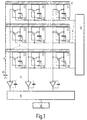
- FIG. 1 A sensor is provided for each pixel (pixel), which comprises a switching element 1, a capacitance 2 and a photosensor.
- the typically 2000 x 2000 switching elements are realized on a common dielectric substrate (glass) using thin-film technology (for example in the form of thin-film field-effect transistors 1, as indicated in FIG. 1).
- the photosensors are covered by a continuous photoconductor layer 3 covering the entire image field.
- a bias electrode 4 which is applied to the photoconductor layer and for each picture element a separate collecting electrode 11 is located on the other side of the photoconductor layer.
- the sensors are arranged in rows and columns in the manner of a matrix, the distance between the rows and the columns being the same. This distance determines the spatial resolution.
- the gate electrodes of the thin-film field effect transistors forming the switching elements are switched through line by line by means of a control circuit 6.
- the gate electrodes of all switching elements of a row are each connected to a common switching line 5.
- the source electrodes of the thin-film field effect transistors are each connected to the capacitance assigned to them, while their drain electrodes are connected in columns to a common output line 7.
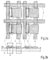
- the ground line 10 and the switching lines 5 are applied to a substrate 15.
- the switching lines 5 are provided with vertical taps 17, which form the gate electrodes of the thin-film field-effect transistors.
- the electrode 11 thus has the function of the collecting and the source electrode, and in addition, together with a ground line 10 covered by it and a dielectric in between, it forms the storage capacitance 2.
- the layers between the electrodes are very thin (in the order of magnitude of 0.2-1 ⁇ m). It is therefore important that the collecting electrodes 11 do not cover the switching lines 5, but in particular the output lines 7, because large parasitic capacitances would form between the collecting electrode 11 and the relevant electrodes. In the case of the output lines 7, this would lead to a capacitive signal decoupling and thus to a reduction in the readable signal and to increased noise of those connected to the output lines 7 Output amplifier 8 since they "see" a larger input capacitance.
- the collecting electrodes 11, on the one hand, and the lines 5, 7, on the other hand, must therefore be arranged next to one another, ie the top view of the collecting electrodes may, according to FIG. Fig. 2a do not overlap with lines 5 and 7. You must therefore restrict yourself to the area remaining between two adjacent switching lines 5 or two adjacent output lines 7.
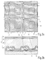
- the collecting electrodes each comprise two electrode parts which are in electrical contact with one another, in that the first electrode part is arranged in a region next to the output line, in that the second electrode part has a larger area as the first electrode part and located between it and the bias electrode, and that there is an insulating layer between the second electrode part and the output line.
- the first electrode part forms a capacitance together with one of the reference or ground electrodes 10 and at the same time represents an electrode of the switching element, while the second electrode part generates those in the photoconductor layer Collects load carriers.
- the restrictions to which the first electrode part is subject do not apply to this second electrode part, ie the second electrode part can at least partially cover the lines, in particular the output lines, so that there is a comparatively high sensitivity.
- the parasitic capacitances resulting between this second electrode part and the lines can be kept small by making the insulating layer sufficiently thick.
- JP-OS 61-1177 or US Pat. No. 4,471,371 which relates to a thin-film image detector for visible light.
- Image detectors for visible light differ from X-ray image detectors in that instead of a relatively thick photoconductor layer they only have a thin semiconductor layer, for example made of amorphous silicon. This results in a relatively large capacity, so that a separate capacity - such as capacity 2 - is not required.
- the electrodes of the switching elements or the output line are located in a plane which is separated from the plane in which the collecting electrodes are located by an insulating layer produced using thin-film technology. This results in very high parasitic capacitances between the electrodes of the switching element and the collecting electrode, which cannot be tolerated in an X-ray image detector which is said to be readable with a high image frequency.
- a further development of the invention which is suitable for both solutions provides that layers are provided on both sides of the photoconductor layer with a small thickness compared to the photoconductor, which are doped in such a way that they provide one for the charge carriers which flow from the photoconductor to the electrodes adjacent to them have high conductivity compared to the conductivity for charge carriers with the opposite polarity.
- the two layers on both sides of the photoconductor layer block charge carriers injected from the collecting electrodes or from the biasing electrode, as a result of which the dark discharge rates are reduced.
- a layer is applied between the bias electrode and the layer adjacent to it, which layer consists of the same material as the photoconductor layer, but is considerably thinner than this. As a result, the dark discharge rates are once again significantly reduced.
- an insulating layer 13 with a flat end surface is first applied to the thin-film structure shown in FIG. 2. In this end surface, contact holes are made above the collecting electrodes 11 by means of photolithographic processes, which reach as far as the electrodes 11.
- a metallic layer is then applied, for example by deposition from the vapor phase.
- This continuous layer of preferably aluminum is then structured by means of a photolithographic process in such a way that electrodes 14 which are as large as possible are formed for the individual pixels, which electrodes cover the area available for one pixel as completely as possible and which through the contact holes with the electrodes underneath 11 have electrical contact.
- the distance between the facing each other Edges of adjacent collecting electrodes can be between 5 and 15 ⁇ m, so that the ratio between the collecting electrode area and the area available for a pixel can still be up to 90% even with a pixel size of 100 ⁇ m.
- the electrodes 14 can thus capture a much larger part of the charge carriers generated in the photoconductor than the electrodes 11, so that there is an improved sensitivity.
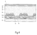
- the insulating layer 13 must have a thickness of at least 3 ⁇ m, preferably 5 to 10 ⁇ m. A relative dielectric constant of 4 to 5 is assumed (with a higher dielectric constant, the insulating layer must be even larger). Silicon oxide, silicon nitride or polyimide are suitable materials.
- the insulating layer is preferably applied in several individual layers, each with a smaller thickness. This is shown in FIG. 4, the insulating layer being formed by the sub-layers 131 and 132.
- the contact holes provided for the purpose of contacting the electrode parts 11 and 14 preferably have an increasing size, so that there are steps which ensure good metallization through the layer 14. It can be advantageous to use different materials for the different sublayers (for example, layer 131 can be made of silicon oxide and layer 132 can be made of polyimide). If etching agents are then used in the etching process required to produce the contact holes, each of which attacks only one of the partial layers, then it is easily possible to stop the etching process at a defined depth for the individual layers.
- the actual photoconductor layer 3 is then applied to the structure formed after the electrodes 14 have been applied.
- the photoconductor layer 3 is finally provided with a metallic cover electrode 4 made of gold or aluminum. It can prove advantageous to construct the photoconductor as a multilayer structure as follows:
- a semiconducting layer 31 is applied, which practically does not conduct negative charge carriers, but positive charge carriers all the better.
- This layer can consist of different materials, such as HgI 2 , CdSe, CdTe, PbO or Se, the conductivity of which is set by certain additives in the above sense. This is achieved, for example, with a 1-5 ⁇ m thick selenium layer doped with 20 to 200 ppm Cl.
- the actual photoconductor layer 32 made of amorphous selenium is then deposited with an addition of 0.1 to 1% arsenic. This layer must be between 200 and 800 ⁇ m thick in order to be able to sufficiently absorb the X-ray quanta that result from a medical examination.
- a semiconductor layer 33 is applied to the layer 32 and is doped in such a way that it does not conduct positive charge carriers, that is to say holes, but the better the negative charge carriers (electrons).
- This layer can consist, for example, of selenium which consists of 20 to 200 ppm alkali metal (Li, Na, K, Cs) and has a thickness between 0.5 and 2 ⁇ m.
- a positive voltage between 1 and 10 kV is applied to the bias electrode 4.
- the semiconductor layers 31 and 33 are then intended to block the charge carriers which may be injected from the collecting electrodes 14 or the top electrode 4, so that the dark discharge rates are decisively reduced.
- this function is only satisfactorily fulfilled if there is still a thin semiconducting layer between the doped layer 33 and the bias electrode 4 made of gold or aluminum, which is not very conductive for negative and positive charge carriers, for example a selenium layer, which coexists in the same way Arsenic is doped like the actual photoconductor layer 32.
- This means that the thickness of the layer 32 of 0.3 mm up to 5 kV are applied to the bias electrode without there being any significant dark currents (with a density of more than 1 pA / cm 2 ).
- An X-ray image is read out with such an X-ray image detector in a manner similar to that described in EP-OS 444 720.
- the switching elements 1 are closed (conductive) so that the capacitors 2 cannot charge.
- the X-ray exposure can be carried out with an image frequency of e.g. 60 frames / sec take place, the dose for the images should be between 10 nGy and 50 ⁇ Gy.
- Switches 1 are normally open during the X-ray exposure. To read out the x-ray image, all switching elements of a single line are closed simultaneously for a short time (10 to 20 ⁇ s) by applying a corresponding potential to the associated switching line 5. During this time, the charges collected from the capacitors 2 flow via the output lines 7 to the inputs of the amplifiers 8. The amplifiers are connected as current integrators, so that their output signal corresponds to the total charge that has flowed from the capacitor. The collecting electrodes 11, 14 are virtually kept at ground potential. The output signals of the amplifiers are taken over by an analog multiplexer 9, which deforms a serial signal stream with a correspondingly higher bandwidth from the parallel signals. The entire process is then repeated for the next and successively for all other image lines.
- the amplifiers 8 cannot currently be realized with the required sensitivity and low noise in thin-film technology. They must therefore be located outside the thin film substrate and implemented using conventional integrated circuit technology. Approx. 32 to 256 amplifiers with the associated analog multiplexer can be integrated on one chip. For a total of 2000 image columns, between 8 and 64 chips of this type would then be required, the inputs of which should be connected to the output lines located on the thin-film substrate would be. The outputs of the analog multiplexers are connected to analog-digital converters, after which the digital data are further processed.
- the insulating layer 13 is produced with a layer thickness customary for thin-layer technology (between 0.5 ⁇ m and a maximum of 2 ⁇ m), a contact hole extending up to the collecting electrode 11 being provided above each of the collecting electrodes.
- Analog structures can also be realized in other semiconductor materials such as HgI 2 , CdTe, CDSe or PbO.
- a negative voltage is applied to the bias electrode, so that negative charge carriers (electrons) migrate to the collecting electrode during X-ray exposure, the layers with good conductivity for positive charge carriers (holes) and poor conductivity for electrons are closed swap and vice versa.
- a semiconducting layer 35 is applied to the insulating layer 13, which does not conduct the negative charge carriers, but has a good conductivity for positive charge carriers.
- it is a selenium layer which - like layer 31 - is doped with 20 to 200 ppm CI, but which is thicker than layer 31 of FIG. 3, for example 5 to 40 ⁇ m.
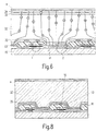
- FIG. 6 corresponds to FIG. 5b, but the electrical field lines or the paths of the electrical charge carriers are shown.
- a positive voltage of, for example, 3 kV is applied to the bias electrode 4 and charge carriers are generated in the photoconductor layer 32, here for example selenium doped with 0.1 to 1% arsenic, by X-ray exposure, positive space charges form above the areas passivated by the insulating layer 13. As a result, the electric field is deformed, as indicated in FIG. 6. Because of the good conductivity of layer 35 for holes, even charge carriers that were not generated above the collecting electrode can now reach the collecting electrode at high speed in this layer. Possibly. Electrons injected from the collecting electrodes 11 are held in the layer 35; at this point the layer acts analogously to layer 31 in FIGS. 3 and 4.
- the good conductivity of layer 35 for positive charge carriers at the same time means that the space charge in this layer can easily flow apart, as is outlined in FIG. 6.
- the desired field distortion will be relatively low in the state of equilibrium.
- the field distortion can extend into the actual photoconductor layer 32.
- this has a low conductivity for the positive charge carriers, which inhibits the transport to the collecting electrode.
- FIG. 7 A further development of this detector is shown in Figure 7.
- a further semiconductor layer 36 is inserted under the layer which is good for holes and poorly for electrons and which has approximately equally low conductivity for both polarities of charge carriers.
- this layer is approximately 1-40 ⁇ m thick and consists of selenium, doped with 0.1 to 1% arsenic. Because of its lower conductivity for positive charge carriers, the space charge builds up more efficiently because it cannot flow apart parallel to the substrate. The field bending is thus forced and to a large extent localized in the layer 35, which is highly conductive for holes. The transfer of the charge carriers to the collecting electrode, which now takes place predominantly in the layer 35 which is conductive for holes, is thus made possible in such a way that a maximum signal is obtained in a short time.
- electrons injected from the collecting electrodes are held in the layer 35. The fact that they have previously passed through layer 36 is irrelevant to the functionality of the detector.
- the collecting electrodes can each comprise an additional electrode part 16, which - as shown in FIG. 8 - covers the associated thin film transistor above the insulating layer 13 and which is in electrical contact with the electrode part 11.
- These electrode parts are produced by metallizing the surface, which arises after the application of the insulating layer and the application of the contact holes but before the application of the semiconducting layer 35.
Landscapes
- General Physics & Mathematics (AREA)
- Engineering & Computer Science (AREA)
- Signal Processing (AREA)
- Physics & Mathematics (AREA)
- Health & Medical Sciences (AREA)
- Life Sciences & Earth Sciences (AREA)
- Molecular Biology (AREA)
- High Energy & Nuclear Physics (AREA)
- Multimedia (AREA)
- Spectroscopy & Molecular Physics (AREA)
- Measurement Of Radiation (AREA)
- Solid State Image Pick-Up Elements (AREA)
- Light Receiving Elements (AREA)
- Conversion Of X-Rays Into Visible Images (AREA)
Description
Die Erfindung betrifft einen Röntgenbilddetektor mit einer Vielzahl von für Röntgenstrahlung empfindlichen Sensoren mit folgenden Merkmalen:
- Jeder Sensor enthält eine Sammelelektrode und ein Schaltelement, das die Sammelelektrode mit einer Ausgangsleitung verbindet;
- zwischen den einzelnen Sammelelektroden und einer Vorspannungselektrode befindet sich eine Photoleiterschicht;
- die Sammelelektroden bilden zusammen mit Bezugselektroden Kapazitäten, die durch im Photoleiter erzeugte Ladungsträger aufladbar sind.
- Each sensor contains a collecting electrode and a switching element that connects the collecting electrode to an output line;
- there is a photoconductor layer between the individual collecting electrodes and a bias electrode;
- the collecting electrodes together with reference electrodes form capacities which can be charged by charge carriers generated in the photoconductor.
Mit derartigen Röntgenbilddetektoren sollen u.a. Durchleuchtungen durchgeführt werden, bei denen Röntgenaufnahmen in dichter zeitlicher Folge, z.B. 60 Bilder / sec. anfallen. Ein solcher Röntgenbilddetektor, der aus der EP-OS 444 720 (PHD 90-016 EP) bekannt ist, ist in Fig. 1 schematisch dargestellt. Für jeden Bildpunkt (Pixel) ist ein Sensor vorgesehen, der ein Schaltelement 1, eine Kapazität 2 sowie einen Photosensor umfaßt. Die typischerweise 2000 x 2000 Schaltelemente werden auf einem gemeinsamen dielektrischen Substrat (Glas) in Dünnschichttechnik realisiert (beispielsweise in Form von Dünnfilm- Feldeffekttransistoren 1, wie in Fig. 1 angedeutet.) Die Photosensoren werden durch eine durchgehende, das ganze Bildfeld bedeckende Photoleiterschicht 3, eine Vorspannungselektrode 4, die auf die Photoleiterschicht aufgebracht ist und für jedes Bildelement eine gesonderte, auf der anderen Seite der Photoleiterschicht befindliche Sammelelektrode 11 gebildet. Wenn im Betriebszustand der Bilddetektor von Röntgenstrahlung getroffen wird, werden in der Photoleiterschicht 3 Ladungsträger erzeugt, die unter dem Einfluß eines elektrischen Feldes, das mittels einer an die Vorspannungselektrode 4 angeschlossenen Vorspannungsquelle 40 erzeugt wird, durch den Photoleiter zu den Sammelelektroden 11 fließen. Dadurch werden die mit den Sammelelektroden 11 verbundenen Kapazitäten 2 aufgeladen, deren andere Elektrode an eine Elektrode 10 auf Bezugspotential angeschlossen ist.With such X-ray image detectors, fluoroscopy is to be carried out, inter alia, in which X-ray recordings occur in close chronological order, for example 60 images / sec. Such an X-ray image detector, which is known from EP-OS 444 720 (PHD 90-016 EP), is shown schematically in FIG. 1. A sensor is provided for each pixel (pixel), which comprises a
Die Sensoren sind nach Art einer Matrix zeilen- und spaltenweise angeordnet, wobei der Abstand der Zeilen und der Spalten voneinander gleich ist. Dieser Abstand bestimmt das räumliche Auflösungsvermögen. Zum Auslesen werden mittels einer Ansteuerschaltung 6 die Gate-Elektroden der die Schaltelemente bildenden Dünnfilm-Feldeffekttransistoren zeilenweise durchgeschaltet. Zu diesem Zweck sind die Gate-Elektroden aller Schaltelemente einer Zeile jeweils mit einer gemeinsamen Schaltleitung 5 verbunden. Die Source-Elektroden der Dünnfilm-Feldeffekttransistoren sind jeweils mit der ihnen zugeordneten Kapazität verbunden, während ihre Drain-Elektroden spaltenweise an einer gemeinsamen Ausgangsleitung 7 angeschlossen sind.The sensors are arranged in rows and columns in the manner of a matrix, the distance between the rows and the columns being the same. This distance determines the spatial resolution. For reading out, the gate electrodes of the thin-film field effect transistors forming the switching elements are switched through line by line by means of a control circuit 6. For this purpose, the gate electrodes of all switching elements of a row are each connected to a
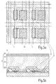
In den Fig. 2a und 2b ist eine Draufsicht bzw. ein Querschnitt von einem Teil des Bilddetektors dargestellt, wobei die Photoleiterschicht 3 und die Vorspannungselektrode 4 weggelassen sind. Die Darstellung ist stark vereinfacht, zeigt aber die wesentlichen Elemente. Auf ein Substrat 15 sind die Masseleitung 10 sowie die Schaltleitungen 5 aufgebracht. Die Schaltleitungen 5 sind mit senkrechten Abgriffen 17 versehen, die die Gate-Elektroden der Dünnfilm-Feldeffekttransistoren bilden. Oberhalb der Gate-Elektrode 17 befindet sich eine Mehrschichtstruktur 12 aus Halbleiter- und Isolierschichten, die zusammen mit den Elektroden 7 (Drain) und 11 (Source) einen Dünnfilm-Feldeffekttransistor bildet. Die Elektrode 11 hat somit die Funktion der Sammel- und der Source-Elektrode, und außerdem bildet sie zusammen mit einer von ihr überdeckten Masseleitung 10 und einem dazwischenliegenden Dielektrikum die Speicherkapazität 2.2a and 2b show a top view or a cross section of part of the image detector, the
Bei der in Dünnschichttechnik realisierten Anordnung nach Fig. 2 sind die Schichten zwischen den Elektroden sehr dünn (in der Größenordnung von 0,2 - 1 µm). Deshalb ist es wichtig, daß die Sammelektroden 11 die Schaltleitungen 5, insbesondere aber die Ausgangsleitungen 7 nicht überdecken, weil sich dadurch große parasitäre Kapazitäten zwischen der Sammelelektrode 11 und den betreffenden Elektroden bilden würden. Dies würde im Falle der Ausgangsleitungen 7 zu einer kapazitiven Signalauskopplung und damit zu einer Verkleinerung des auslesbaren Signals führen sowie zu erhöhtem Rauschen der an die Ausgangsleitungen 7 angeschlossenen Ausgangsverstärker 8, da diese eine größere Eingangskapazität "sehen". Die Sammelelektroden 11 einerseits und die Leitungen 5, 7 andererseits müssen also nebeneinander angeordnet sein, d.h. die Sammelelektroden dürfen sich in der Draufsicht gem. Fig. 2a nicht mit den Leitungen 5 und 7 überlappen. Sie müssen sich also auf die zwischen zwei benachbarten Schaltleitungen 5 bzw. zwei benachbarten Ausgangsleitungen 7 verbleibende Fläche beschränken.2, the layers between the electrodes are very thin (in the order of magnitude of 0.2-1 μm). It is therefore important that the collecting
Da alle Leitungen 5, 7 und 10 eine Breite zwischen 10 und 25 µm aufweisen müssen, um eine genügend hohe Leitfähigkeit zu erreichen, bedeutet dies, daß der Anteil der Sammelelektroden an der Gesamtfläche eines Röntgenbilddetektors umso kleiner ist, je kleiner die Bildpunkte (Pixel) bzw. ihr Abstand voneinander ist, d.h., je größer das Auflösungsvermögen ist.Since all
Aufgabe der vorliegenden Erfindung ist es, einen Röntgenbilddetektor zu schaffen, der auch bei hohem räumlichen Auflösungsvermögen eine gute Empfindlichkeit bei gleichzeitig möglichst kapazitätsarmem Aufbau aufweist.It is an object of the present invention to provide an X-ray image detector which, even with a high spatial resolution, has a good sensitivity and at the same time has the least possible capacity.
Diese Aufgabe wird ausgehend von einem Röntgenbilddetektor der eingangs genannten Art erfindungsgemäß dadurch gelöst, daß die Sammelelektroden je zwei in elektrischen Kontakt miteinander befindliche Elektrodenteile umfassen, daß der erste Elektrodenteil jeweils in einem Bereich neben der Ausgangsleitung angeordnet ist, daß der zweite Elektrodenteil eine größere Fläche hat als der erste Elektrodenteil und sich zwischen diesem und der Vorspannungselektrode befindet, und daß sich zwischen dem zweiten Elektrodenteil und der Ausgangsleitung eine Isolierschicht befindet.This object is achieved on the basis of an X-ray image detector of the type mentioned at the outset in that the collecting electrodes each comprise two electrode parts which are in electrical contact with one another, in that the first electrode part is arranged in a region next to the output line, in that the second electrode part has a larger area as the first electrode part and located between it and the bias electrode, and that there is an insulating layer between the second electrode part and the output line.
Durch die Verwendung einer aus zwei Elektrodenteilen bestehenden Sammelelektrode teilen sich auch deren Funktionen auf: Der erste Elektrodenteil bildet zusammen mit einer der Bezugs- bzw. Masseelektroden 10 eine Kapazität und stellt gleichzeitig eine Elektrode des Schaltelements dar, während der zweite Elektrodenteil die in der Photoleiterschicht erzeugten Ladungsträger sammelt. Für diesen zweiten Elektrodenteil gelten die Beschränkungen nicht, denen der erste Elektrodenteil unterliegt, d.h. der zweite Elektrodenteil kann die Leitungen, insbesondere die Ausgangsleitungen, wenigstens teilweise überdecken, so daß sich eine vergleichsweise große Empfindlichkeit ergibt. Die zwischen diesem zweiten Elektrodenteil und den Leitungen resultierenden parasitären Kapazitäten lassen sich dadurch klein halten, daß die Isolierschicht genügend dick gemacht wird.By using a collecting electrode consisting of two electrode parts, their functions are also divided: the first electrode part forms a capacitance together with one of the reference or
An dieser Stelle sei auf die JP-OS 61-1177 bzw. auf die US-PS 4,471,371 verwiesen, sich auf einen Dünnfilm-Bilddetektor für sichtbares Licht beziehen. Bilddetektoren für sichtbares Licht unterscheiden sich von Röntgenbilddetektoren dadurch, daß sie anstelle einer relativ dicken Photoleiterschicht nur eine dünne Halbleiterschicht aufweisen, beispielsweise aus amorphem Silizium. Dadurch ergibt sich eine relativ große Kapazität, so daß eine gesonderte Kapazität - wie die Kapazität 2 - nicht erforderlich ist. Bei den bekannten Bilddetektoren befinden sich die Elektroden der Schaltelemente bzw. die Ausgangsleitung in einer Ebene, die von der Ebene, in der sich die Sammelelektroden befinden, durch eine in Dünnschichttechnik erzeugte Isolierschicht getrennt ist. Dadurch ergeben sich zwischen den Elektroden des Schaltelements und der Sammelelektrode sehr hohe parasitäre Kapazitäten, die bei einem Röntgenbilddetektor, der mit hoher Bildfrequenz auslesbar sein soll, nicht hingenommen werden können.At this point, reference is made to JP-OS 61-1177 or US Pat. No. 4,471,371, which relates to a thin-film image detector for visible light. Image detectors for visible light differ from X-ray image detectors in that instead of a relatively thick photoconductor layer they only have a thin semiconductor layer, for example made of amorphous silicon. This results in a relatively large capacity, so that a separate capacity - such as capacity 2 - is not required. In the known image detectors, the electrodes of the switching elements or the output line are located in a plane which is separated from the plane in which the collecting electrodes are located by an insulating layer produced using thin-film technology. This results in very high parasitic capacitances between the electrodes of the switching element and the collecting electrode, which cannot be tolerated in an X-ray image detector which is said to be readable with a high image frequency.
Eine zweite Lösung des der Erfindung zugrundeliegenden Problems ist ausgehend von einem Röntgenbilddetektor der eingangs genannten Art gekennzeichnet durch folgende Merkmale:
- Die Sammelelektrode ist neben der Ausgangsleitung angeordnet;
- das Schaltelement und die Ausgangsleitung sind von einer Isolierschicht bedeckt;
- die Isolierschicht und die Sammelelektrode sind von einer halbleitenden Schicht bedeckt;
- die halbleitende Schicht ist so dotiert, daß sie für die in Richtung zur Sammelelektrode fließenden Ladungsträger eine im Vergleich zur Leitfähigkeit für Ladungsträger mit entgegengesetzter Polarität große Leitfähigkeit aufweist.
- The collecting electrode is arranged next to the output line;
- the switching element and the output line are covered by an insulating layer;
- the insulating layer and the collecting electrode are covered by a semiconducting layer;
- the semiconducting layer is doped in such a way that it has a high conductivity for the charge carriers flowing in the direction of the collecting electrode in comparison with the conductivity for charge carriers with opposite polarity.
Bei dieser Lösung bilden sich oberhalb der durch die Isolierschicht passivierten Bereiche in der halbleitenden Schicht Raumladungen, die das elektrische Feld in der Photoleiterschicht so verformen, daß auch Ladungsträger, die nicht oberhalb der mit der halbleitenden Schicht in Kontakt stehenden Sammelelektroden erzeugt werden, diese erreichen können. Trotz vergleichsweise kleiner Flächen der Sammelelektroden ergibt auch diese Lösung eine gute Empfindlichkeit. In weiterer Ausgestaltung dieser Lösung ist vorgesehen, daß sich zwischen der halbleitenden Schicht und den Sammelelektroden eine zusätzliche halbleitende Schicht befindet, die sowohl für positive als auch für negative Ladungsträger eine geringe Leitfähigkeit aufweist. Diese zusätzliche halbleitende Schicht dient zum Aufbau einer Raumladung im Bereich neben den Sammelelektroden. Die Raumladung verzerrt das elektrische Feld derart, daß die signalgebenden Ladungsträger in der darüber liegenden halbleitenden Schicht, die für diese eine gute Leitfähigkeit hat, zur Sammelelektrode transportiert werden - und zwar auch dann, wenn sie nicht im Bereich oberhalb der Sammelelektrode erzeugt wurden.In this solution, space charges form above the areas passivated by the insulating layer in the semiconducting layer, which deform the electric field in the photoconductor layer in such a way that charge carriers which are not generated above the collecting electrodes which are in contact with the semiconducting layer can reach them . Despite the comparatively small areas of the collecting electrodes, this solution also gives good sensitivity. In a further embodiment of this solution, it is provided that there is an additional semiconducting layer between the semiconducting layer and the collecting electrodes, which has a low conductivity for both positive and negative charge carriers. This additional semiconducting layer is used to build up a space charge in the area next to the collecting electrodes. The space charge distorts the electric field in such a way that the signaling charge carriers in the overlying semiconducting layer, which has good conductivity for them, are transported to the collecting electrode - even if they were not generated in the area above the collecting electrode.
Eine für beide Lösungen geeignete Weiterbildung der Erfindung sieht vor, daß beiderseits der Photoleiterschicht Schichten mit einer im Vergleich zum Photoleiter geringen Dicke vorgesehen sind, die so dotiert sind, daß sie für die Ladungsträger, die aus dem Photoleiter auf die ihnen benachbarten Elektroden zufließen, eine im Vergleich zur Leitfähigkeit für Ladungsträger mit der entgegengesetzten Polarität große Leitfähigkeit aufweisen. Die beiden Schichten beiderseits der Photoleiterschicht blockieren von den Sammelelektroden oder von der Vorspannungselektrode injizierte Ladungsträger, wodurch die Dunkelentladungsraten verringert werden. In weiterer Ausgestaltung ist vorgesehen, daß zwischen der Vorspannungselektrode und der ihr benachbarten Schicht eine Schicht angebracht ist, die aus dem gleichen Material besteht wie die Photoleiterschicht, aber wesentlich dünner ist als diese. Dadurch werden die Dunkelentladungsraten noch einmal entscheidend verringert.A further development of the invention which is suitable for both solutions provides that layers are provided on both sides of the photoconductor layer with a small thickness compared to the photoconductor, which are doped in such a way that they provide one for the charge carriers which flow from the photoconductor to the electrodes adjacent to them have high conductivity compared to the conductivity for charge carriers with the opposite polarity. The two layers on both sides of the photoconductor layer block charge carriers injected from the collecting electrodes or from the biasing electrode, as a result of which the dark discharge rates are reduced. In a further embodiment it is provided that a layer is applied between the bias electrode and the layer adjacent to it, which layer consists of the same material as the photoconductor layer, but is considerably thinner than this. As a result, the dark discharge rates are once again significantly reduced.
Die Erfindung wird nachstehend anhand der Zeichnungen näher erläutert. Es zeigen:
- Fig. 1
- ein Schaltschema des erfindungsgemäßen, bzw. des bekannten Röntgenbilddetektors.
- Fig. 2
- eine Dünnschichtstruktur eines solchen Detektors in der Draufsicht (Fig. 2a) und im Querschnitt (Fig. 2b).
- Fig. 3
- eine erste Ausführungsform eines erfindungsgemäßen Detektors in der Draufsicht (Fig. 3a) und im Querschnitt (Fig. 3b).
- Fig. 4
- eine verbesserte Ausführungsform eines solchen Detektors im Querschnitt.
- Fig. 5
- eine andere Ausführungsform eines erfindungsgemäßen Detektors in der Draufsicht (Fig. 5a) und im Querschnitt (Fig. 5b).
- Fig. 6
- die elektrischen Feldlinien bei der Anordnung nach Fig. 5b und
- Fig. 7
- eine verbesserte Ausführungsform im Querschnitt.
- Fig. 8
- eine verbesserte Ausführungsform im Querschnitt.
- Fig. 1
- a circuit diagram of the inventive or the known X-ray image detector.
- Fig. 2
- a thin-film structure of such a detector in plan view (Fig. 2a) and in cross section (Fig. 2b).
- Fig. 3
- a first embodiment of a detector according to the invention in plan view (Fig. 3a) and in cross section (Fig. 3b).
- Fig. 4
- an improved embodiment of such a detector in cross section.
- Fig. 5
- another embodiment of a detector according to the invention in plan view (Fig. 5a) and in cross section (Fig. 5b).
- Fig. 6
- the electrical field lines in the arrangement of Fig. 5b and
- Fig. 7
- an improved embodiment in cross section.
- Fig. 8
- an improved embodiment in cross section.
Bei der in Fig. 3 in der Draufsicht bzw. im Querschnitt dargestellten Ausführungsform eines Röntgenbilddetektors sind für gleiche Teile die gleichen Bezugszeichen verwendet wie in Fig. 2. Der in Fig. 3b dargestellte Querschnitt ist nicht maßstäblich und auch die Relationen zwischen den Dicken der einzelnen Schichten entsprechen nicht den tatsächlichen Verhältnissen, die sich aus der folgenden Beschreibung ergeben. Auf die in Fig. 2 dargestellte Dünnschichtstruktur wird zunächst eine isolierende Schicht 13 mit einer ebenen Abschlußfläche aufgebracht. In dieser Abschlußfläche werden oberhalb der Sammelelektroden 11 mit Hilfe von photolithographischen Verfahren Kontaktlöcher angebracht, die bis zu den Elektroden 11 reichen.In the embodiment of an x-ray image detector shown in plan view or in cross section in FIG. 3, the same reference numerals are used for the same parts as in FIG. 2. The cross section shown in FIG. 3b is not to scale and also the relationships between the thicknesses of the individual Layers do not correspond to the actual conditions that result from the following description. An insulating
Danach wird eine metallische Schicht aufgebracht, beispielsweise durch Abscheiden aus der Dampfphase. Diese durchgehende Schicht aus vorzugsweise Aluminium wird dann durch ein photolitographisches Verfahren so strukturiert, daß für die einzelnen Bildpunkte möglichst großflächige Elektroden 14 entstehen, die die für jeweils einen Bildpunkt zur Verfügung stehende Fläche möglichst vollständig bedecken und die durch die Kontaktlöcher hindurch mit den darunter befindlichen Elektroden 11 elektrischen Kontakt haben. Der Abstand zwischen den einander zugewandten Kanten benachbarter Sammelelektroden kann dabei zwischen 5 und 15 µm liegen, so daß das Verhältnis zwischen der Sammelelektrodenfläche und der für einen Bildpunkt zur Verfügung stehenden Fläche auch bei einer Bildpunktgröße von 100 µm noch bis zu 90 % betragen kann. Die Elektroden 14 können somit einen wesentlich größeren Teil der im Photoleiter erzeugten Ladungsträger auffangen als die Elektroden 11, so daß sich eine verbesserte Empfindlichkeit ergibt.A metallic layer is then applied, for example by deposition from the vapor phase. This continuous layer of preferably aluminum is then structured by means of a photolithographic process in such a way that
Bei diesen Abmessungen der die Elektroden 11 allseits überdeckenden Elektroden 14, ist es unausbleiblich, daß sie auch die Ausleseleitungen und die Ansteuerleitungen - zumindest teilweise - überdecken, womit sich zusätzliche parasitäre Kapazitäten zwischen der Elektrode 11 sowie den Leitungen 7 und 5 ausbilden. Um diese parasitären Kapazitäten möglichst klein zu halten, muß die isolierende Schicht 13 eine Dicke von mindestens 3 µm, vorzugsweise 5 bis 10 µm aufweisen. Dabei wird von einer relativen Dielektrizitätskonstanten von 4 bis 5 ausgegangen, (bei einer höheren Dielektrizitätskonstanten muß die isolierende Schicht noch größer sein). Als geeignete Materialien kommen Siliziumoxid, Siliziumnitrid oder Polyimid in Frage.With these dimensions of the
Um diese relativ großen Schichtdicken zu erreichen, wird die Isolierschicht bevorzugt in mehreren Einzelschichten von jeweils geringerer Dicke aufgebracht. Dies ist in Fig. 4 dargestellt, wobei die isolierende Schicht durch die Teilschichten 131 und 132 gebildet wird. Die zwecks Kontaktierung der Elektrodenteile 11 und 14 vorgesehenen Kontaktlöcher haben dabei vorzugsweise eine nach oben hin zunehmende Größe, so daß sich Stufen ergeben, die eine gute Metallisierung durch die Schicht 14 gewährleisten. Dabei kann es von Vorteil sein, für die verschiedenen Teilschichten unterschiedliche Materialien zu verwenden (z.B. kann die Schicht 131 aus Siliziumoxid und die Schicht 132 aus Polyimid bestehen). Verwendet man dann bei dem zur Herstellung der Kontaktlöcher erforderlichen Ätzprozeß Ätzmittel, die jeweils nur eine der Teilschichten angreifen, dann ist es leicht möglich, für die einzelnen Schichten den Ätzprozeß in einer definierten Tiefe zu stoppen.In order to achieve these relatively large layer thicknesses, the insulating layer is preferably applied in several individual layers, each with a smaller thickness. This is shown in FIG. 4, the insulating layer being formed by the
Auf die nach dem Aufbringen der Elektroden 14 entstandene Struktur wird dann die eigentliche Photoleiterschicht 3 aufgebracht. Die Photoleiterschicht 3 wird abschließend mit einer metallischen Deckelektrode 4 aus Gold oder Aluminium versehen. Dabei kann es sich als vorteilhaft erweisen, den Photoleiter als Mehrschichtstruktur folgendermaßen aufzubauen:The
Zunächst wird eine halbleitende Schicht 31 aufgebracht, die negative Ladungsträger praktisch nicht leitet, dafür positive Ladungsträger umso besser. Diese Schicht kann aus verschiedenen Materialien, wie z.B. HgI2, CdSe, CdTe, PbO oder Se bestehen, deren Leitfähigkeit durch bestimmte Zusätze in obigem Sinn eingestellt wird. Dies wird beispielsweise mit einer 1 - 5 µm dicken Selenschicht erreicht, die mit 20 bis 200 ppm Cl dotiert ist. Darauf wird die eigentliche Photoleiterschicht 32 aus amorphen Selen mit einem Zusatz von 0,1 bis 1 % Arsen abgeschieden. Diese Schicht muß zwischen 200 und 800 µm dick sein, um die Röntgenquanten, die sich bei einer medizinischen Untersuchung ergeben, ausreichend absorbieren zu können. Auf die Schicht 32 wird eine Halbleiterschicht 33 aufgebracht, die so dotiert ist, daß sie positive Ladungsträger, also Löcher (holes) nicht leitet, dafür umso besser die negativen Ladungsträger (Elektronen). Diese Schicht kann z.B. aus Selen bestehen, das mit 20 bis 200 ppm Alkalimetall (Li, Na, K, Cs) bestehen und eine Dicke zwischen 0,5 und 2 µm aufweisen.First, a
Während des Betriebes des Bilddetektors wird eine positive Spannung zwischen 1 und 10 kV an die Vorspannungselektrode 4 angelegt. Die Halbleiterschichten 31 und 33 sollen dann die Ladungsträger blockieren, die evtl. von den Sammelelektroden 14 oder der Deckelektrode 4 injiziert werden, so daß die Dunkelentladungsraten entscheidend reduziert werden. Erstaunlicherweise wird diese Funktion aber nur dann zufriedenstellend erfüllt, wenn zwischen der dotierten Schicht 33 und der Vorspannungselektrode 4 aus Gold oder Aluminium noch eine dünne halbleitende Schicht, die für negative und positive Ladungsträger wenig leitend ist, z.B. eine Selenschicht, die auf die gleiche Weise mit Arsen dotiert ist wie die eigentliche Photoleiterschicht 32. Damit können bei einer Dicke der Schicht 32 von 0,3 mm bis zu 5 kV an die Vorspannungselektrode angelegt werden, ohne daß es nennenswerte Dunkelströme (mit einer Dichte von mehr als 1 pA/cm2) gibt.During operation of the image detector, a positive voltage between 1 and 10 kV is applied to the
Das Auslesen eines Röntgenbildes mit einem derartigen Röntgenbilddetektor erfolgt in ähnlicher Weise wie in der EP-OS 444 720 beschrieben. Bevor die Röntgenstrahlung eingeschaltet wird, sind die Schaltelemente 1 geschlossen (leitend), so daß sich die Kapazitäten 2 nicht aufladen können. Die Röntgenbelichtung kann mit einer Bildfrequenz von z.B. 60 Bildern/sec erfolgen, wobei die Dosis für die Bilder zwischen 10 nGy und 50 µGy liegen soll.An X-ray image is read out with such an X-ray image detector in a manner similar to that described in EP-OS 444 720. Before the X-ray radiation is switched on, the
Während der Röntgenbelichtung sind die Schalter 1 normalerweise geöffnet. Zum Auslesen des Röntgenbildes werden jeweils alle Schaltelemente einer einzigen Zeile gleichzeitig für eine kurze Zeit (10 bis 20 µs) geschlossen, indem an die zugehörige Schaltleitung 5 ein entsprechendes Potential angelegt wird. Während dieser Zeit fließen die aus den Kapazitäten 2 gesammelten Ladungen über die Ausgangsleitungen 7 auf die Eingänge der Verstärker 8. Die Verstärker sind als Stromintegratoren geschaltet, so daß ihr Ausgangssignal der gesamten vom Kondensator abgeflossenen Ladung entspricht. Dabei werden die Sammelelektroden 11, 14 virtuell auf Erdpotential gehalten. Die Ausgangssignale der Verstärker werden von einem Analogmultiplexer 9 übernommen, der aus den parallel anstehenden Signalen einen seriellen Signalstrom mit entsprechend höherer Bandbreite verformt. Der gesamte Vorgang wird danach für die nächste und sukzessive für alle übrigen Bildzeilen wiederholt.
Die Verstärker 8 können derzeit nicht mit der erforderlichen Empfindlichkeit und Rauscharmut in Dünnschichttechnik realisiert werden. Sie müssen sich daher außerhalb des Dünfilmsubstrats befinden und in konventioneller integrierter Schaltungstechnik realisiert sein. Dabei können jeweils ca. 32 bis 256 Verstärker mit dem zugehörigen Analog-Multiplexer auf einem Chip integriert sein. Für die insgesamt 2000 Bildspalten würden danach also zwischen 8 und 64 derartiger Chips benötigt, deren Eingänge mit denen auf dem Dünnfilmsubstrat befindlichen Ausgangsleitungen zu verbinden wären. Die Ausgänge der Analog-Multiplexer werden mit Analog-Digital-Wandlern verbunden, wonach die digitalen Daten weiterverarbeitet werden.The
In Fig. 5 ist eine zweite Ausführungsform eines Bilddetektors dargestellt, die sich einfacher herstellen läßt. Die Isolierschicht 13 ist dabei mit einer für Dünnschichttechnik üblichen Schichtdicke (zwischen 0,5 µm und maximal 2 µm) hergestellt, wobei oberhalb jeder der Sammelelektroden jeweils ein bis auf die Sammelelektrode 11 reichendes Kontaktloch vorgesehen ist.5 shows a second embodiment of an image detector which is easier to manufacture. The insulating
Im folgenden wird am Beispiel des Photoleiters Se eine mögliche Realisierung erörtert. Analoge Strukturen sind auch in anderen Halbleitermaterialien wie z.B. HgI2, CdTe, CDSe oder PbO zu verwirklichen. Für den Fall, daß - entgegen diesem Beispiel - an die Vorspannungselektrode eine negative Spannung angelegt wird, so daß bei Röntgenbelichtung negative Ladungsträger (Elektronen) zur Sammelelektrode wandern, sind die Schichten mit guter Leitfähigkeit für positive Ladungsträger (Löcher) und schlechter Leitfähigkeit für Elektronen zu vertauschen und umgekehrt. Auf die isolierende Schicht 13 wird eine halbleitende Schicht 35 aufgebracht, die die negativen Ladungsträger nicht leitet, aber eine gute Leitfähigkeit für positive Ladungsträger aufweist. In diesem Beispiel ist es eine Selenschicht, die - wie die Schicht 31 - mit 20 bis 200 ppm CI dotiert ist, die aber dicker ist als die Schicht 31 der Fig. 3, z.B. 5 bis 40 µm. Für die sich daran anschließenden Schichten 32, 33, 34 und 4 gilt, was in Verbindung mit Fig. 3 ausgeführt wurde.A possible implementation is discussed below using the example of the photoconductor Se. Analog structures can also be realized in other semiconductor materials such as HgI 2 , CdTe, CDSe or PbO. In the event that - contrary to this example - a negative voltage is applied to the bias electrode, so that negative charge carriers (electrons) migrate to the collecting electrode during X-ray exposure, the layers with good conductivity for positive charge carriers (holes) and poor conductivity for electrons are closed swap and vice versa. A
Die Funktionsweise dieser Ausführungsform wird nachstehend anhand von Fig. 6 näher erläutert. Fig. 6 entspricht Fig. 5b, wobei jedoch die elektrischen Feldlinien bzw. die Bahnen der elektrischen Ladungsträger eingezeichnet sind.The mode of operation of this embodiment is explained in more detail below with reference to FIG. 6. FIG. 6 corresponds to FIG. 5b, but the electrical field lines or the paths of the electrical charge carriers are shown.
Wird an die Vorspannungselektrode 4 eine positive Spannung von z.B. 3 kV angelegt und werden durch Röntgenbelichtung Ladungsträger in der Photoleiterschicht 32, hier z.B. Selen mit 0,1 bis 1 % Arsen dotiert, erzeugt, so bilden sich positive Raumladungen oberhalb der durch die isolierende Schicht 13 passivierten Bereiche. Dadurch wird das elektrische Feld verformt, wie in Fig. 6 angedeutet. Wegen der guten Leitfähigkeit von Schicht 35 für Löcher können nun selbst Ladungsträger, die nicht oberhalb der Sammelelektrode erzeugt wurden, in dieser Schicht mit hoher Geschwindigkeit zur Sammelelektrode gelangen. Evtl. von den Sammelelektroden 11 injizierte Elektronen werden in der Schicht 35 festgehalten; in diesem Punkt wirkt die Schicht analog zur Schicht 31 in Figuren 3 und 4.If a positive voltage of, for example, 3 kV is applied to the
Die gute Leitfähigkeit von Schicht 35 für positive Ladungsträger bewirkt allerdings gleichzeitig, daß die Raumladung in dieser Schicht leicht auseinanderfließen kann, wie es in Figur 6 skizziert ist. Dadurch wird im Gleichgewichtszustand die gewünschte Feldverzerrung relativ gering sein. Zudem kann die Feldverzerrung bis in die eigentliche Photoleiterschicht 32 hereinreichen. Diese hat für die positiven Ladungsträger jedoch eine geringe Leitfähigkeit, was den Transport zur Sammelelektrode hemmt.However, the good conductivity of
Eine Weiterentwicklung dieses Detektors ist in Bild 7 dargestellt. Hier ist unter der für Löcher gut und für Elektronen schlecht leitenden Schicht eine weitere Halbleiterschicht 36 eingefügt, die für beide Polaritäten von Ladungsträgern in etwa gleichermaßen niedrige Leitfähigkeit aufweist. Diese Schicht ist im Beispiel etwa 1 - 40 µm, dick und besteht aus Selen, dotiert mit 0,1 bis 1 % Arsen. Wegen ihrer geringeren Leitfähigkeit für positive Ladungsträger baut sich hier die Raumladung effizienter auf, da sie nicht parallel zum Substrat auseinander fließen kann. Somit wird die Feldverbiegung forciert und zu einem großen Teil in der für Löcher gut leitfähigen Schicht 35 lokalisiert sein. Der Transfer der Ladungsträger zur Sammelelektrode, der nun überwiegend in der für Löcher leitfähigen Schicht 35 stattfindet, ist damit derart ermöglicht, daß in kurzer Zeit ein maximales Signal erhalten wird. Auch hier werden von den Sammelelektroden injizierte Elektronen in der Schicht 35 festgehalten. Daß sie zuvor Schicht 36 durchlaufen haben, spielt für die Funktionalität des Detektors keine Rolle.A further development of this detector is shown in Figure 7. Here a
Die Raumladungen in der halbleitenden Schicht 35 oberhalb der Dünnfilmtransistoren können u.U. Einfluß auf die Funktion dieser Schaltelemente haben. Um diesen Einfluß auszuschalten, können die Sammelelektroden je einen zusätzlichen Elektrodenteil 16 umfassen, der - wie in Fig. 8 dargestellt - oberhalb der Isolierschicht 13 den zugehörigen Dünnfilmtransistor überdeckt und der mit dem Elektrodenteil 11 in elektrischem Kontakt steht. Diese Elektrodenteile werden durch Metallisierung der Oberfläche erzeugt, die nach dem Aufbringen der isolierenden Schicht und dem Anbringen der Kontaktlöcher aber vor dem Aufbringen der halbleitenden Schicht 35 entsteht.The space charges in the
Claims (9)
- An X-ray image detector, comprising a plurality of X-ray sensitive sensors and having the following features:- each sensor comprises a collecting electrode (11) and a switching element (1) which connects the collecting electrode to an output lead (7);- a photoconductor layer (3) is provided between the individual collecting electrodes (11) and a bias electrode (4);- in conjunction with reference electrodes (10), the collecting electrodes form capacitances (2) which are chargeable by charge carriers generated in the photoconductor;characterized in that each of the collecting electrodes comprises two electrically contacting electrode portions (11, 14), the first electrode portion (11) being arranged in a respective area adjoining the associated output lead (7), the second electrode portion (14) having a surface area which is larger than that of the first electrode portion and being situated between the first electrode portion and the bias electrode, an insulating layer being provided between the second electrode portion (14) and the output lead (7).
- An X-ray image detector, comprising a plurality of X-ray-sensitive sensors and having the following features:- each sensor comprises a collecting electrode (11) and a switching element (1) which connects the collecting electrode to an output lead (7);- a photoconductor layer (3) is provided between the individual collecting electrodes (11) and a bias electrode (4);- in conjunction with reference electrodes (10), the collecting electrodes form capacitances (2) which can be charged by charge carriers generated in the photoconductor;characterized in that it also has the following features:- the collecting electrode (11) is arranged adjacent the output lead (7);- the switching element (1) and the output lead are covered by an insulating layer (13);- the insulating layer (13) and the collecting electrode (11) are covered by a semiconductor layer (35);- the semiconductor layer (35) is doped so that for the charge carriers flowing in the direction of the collecting electrode it has a conductivity which is high in comparison with its conductivity for charge carriers of opposite polarity.
- An X-ray image detector as claimed in Claim 2, characterized in that between the semiconductor layer (35) and the collecting electrodes (11) there is provided an additional semiconductor layer (36) which has a low conductivity for positive as well as negative charge carriers.
- An X-ray image detector as claimed in Claim 2, characterized in that each of the collecting electrodes (11, 16) consists of two electrode portions which electrically contact one another, the first electrode portion being arranged at the area adjacent the output lead, the second electrode (16) being situated on the insulating layer above the associated switching element (1) and itself being covered by the semiconductor layer (35).
- An X-ray image detector as claimed in any one of the preceding Claims, characterized in that the photoconductor layer (32) consists essentially of selenium.
- An X-ray image detector as claimed in any one of the Claims 1 to 4, characterized in that the photoconductor layer consists essentially of one of the substances PbO, CdTe, CdSe or HgI2.
- An X-ray image detector as claimed in any one of the preceding Claims, characterized in that both sides of the photoconductor layer (32) are provided with layers (31, 33) which have a thickness which is small in comparison with that of the photoconductor layer (32), and which are doped so that their conductivity for the charge carriers flowing from the photoconductor layer to the neighbouring electrodes (11; 4) is high in comparison with their conductivity for charge carriers of opposite polarity.
- An X-ray image detector as claimed in Claim 7, characterized in that between the bias electrode (4) and the neighbouring photoconductorlayer (35) there is provided a further layer (34) which is made of the same material as the photoconductor layer but which is substantially thinner than this layer.
- An X-ray image detector as claimed in Claim 1, characterized in that the insulating layer (13) consists of several sub-layers (131, 132) which cover one another and which preferably consist of different materials, the apertures in the insulting layers, through which the two electrode portions (11, 14) contact one another being larger as the sub-layer is situated further from the first electrode portion (11).
Applications Claiming Priority (2)
| Application Number | Priority Date | Filing Date | Title |
|---|---|---|---|
| DE4227096A DE4227096A1 (en) | 1992-08-17 | 1992-08-17 | X-ray image detector |
| DE4227096 | 1992-08-17 |
Publications (3)
| Publication Number | Publication Date |
|---|---|
| EP0588397A2 EP0588397A2 (en) | 1994-03-23 |
| EP0588397A3 EP0588397A3 (en) | 1994-05-04 |
| EP0588397B1 true EP0588397B1 (en) | 1997-06-04 |
Family
ID=6465667
Family Applications (1)
| Application Number | Title | Priority Date | Filing Date |
|---|---|---|---|
| EP93202357A Expired - Lifetime EP0588397B1 (en) | 1992-08-17 | 1993-08-11 | X-ray image detector |
Country Status (4)
| Country | Link |
|---|---|
| US (1) | US5396072A (en) |
| EP (1) | EP0588397B1 (en) |
| JP (1) | JPH06209097A (en) |
| DE (2) | DE4227096A1 (en) |
Families Citing this family (97)
| Publication number | Priority date | Publication date | Assignee | Title |
|---|---|---|---|---|
| GB9414639D0 (en) * | 1994-07-20 | 1994-09-07 | Philips Electronics Uk Ltd | An image detector |
| DE4426451C2 (en) * | 1994-07-26 | 1998-07-16 | Siemens Ag | X-ray diagnostic equipment with a solid-state image converter |
| US5869837A (en) * | 1994-07-27 | 1999-02-09 | Litton Systems Canada Limited | Radiation imaging panel |
| US5498880A (en) * | 1995-01-12 | 1996-03-12 | E. I. Du Pont De Nemours And Company | Image capture panel using a solid state device |
| WO1996034416A1 (en) * | 1995-04-28 | 1996-10-31 | Sunnybrook Hospital | Active matrix x-ray imaging array |
| US5641974A (en) * | 1995-06-06 | 1997-06-24 | Ois Optical Imaging Systems, Inc. | LCD with bus lines overlapped by pixel electrodes and photo-imageable insulating layer therebetween |
| US6124606A (en) * | 1995-06-06 | 2000-09-26 | Ois Optical Imaging Systems, Inc. | Method of making a large area imager with improved signal-to-noise ratio |
| US5648674A (en) * | 1995-06-07 | 1997-07-15 | Xerox Corporation | Array circuitry with conductive lines, contact leads, and storage capacitor electrode all formed in layer that includes highly conductive metal |
| US5619033A (en) * | 1995-06-07 | 1997-04-08 | Xerox Corporation | Layered solid state photodiode sensor array |
| EP0842541B1 (en) | 1995-07-31 | 2002-02-13 | iFire Technology Inc. | Flat panel detector for radiation imaging with reduced trapped charges |
| JP2001509252A (en) * | 1995-07-31 | 2001-07-10 | リットン システムズ カナダ リミテッド | Flat panel detector for radiation imaging with low electronic noise |
| WO1997005657A1 (en) * | 1995-07-31 | 1997-02-13 | Litton Systems Canada Limited | Method and apparatus of operating a dual gate tft electromagnetic radiation imaging device |
| US6232606B1 (en) | 1995-07-31 | 2001-05-15 | Ifire Technology, Inc. | Flat panel detector for radiation imaging and pixel for use therein |
| EP0791230B1 (en) * | 1995-09-12 | 2008-08-13 | Koninklijke Philips Electronics N.V. | X-ray image sensor |
| GB9520791D0 (en) * | 1995-10-13 | 1995-12-13 | Philips Electronics Nv | Image sensor |
| US5733804A (en) * | 1995-12-22 | 1998-03-31 | Xerox Corporation | Fabricating fully self-aligned amorphous silicon device |
| US5717223A (en) * | 1995-12-22 | 1998-02-10 | Xerox Corporation | Array with amorphous silicon TFTs in which channel leads overlap insulating region no more than maximum overlap |
| US5652430A (en) * | 1996-05-03 | 1997-07-29 | Sterling Diagnostic Imaging, Inc. | Direct radiographic imaging panel |
| EP0897597B1 (en) | 1996-05-08 | 2002-09-11 | iFire Technology Inc. | High resolution flat panel for radiation imaging |
| US5770871A (en) * | 1996-06-20 | 1998-06-23 | Xerox Corporation | Sensor array with anticoupling layer between data lines and charge collection electrodes |
| CA2184667C (en) * | 1996-09-03 | 2000-06-20 | Bradley Trent Polischuk | Multilayer plate for x-ray imaging and method of producing same |
| DE19640946A1 (en) * | 1996-10-04 | 1998-04-16 | Philips Patentverwaltung | X-ray arrangement with a photoconductor |
| DE69731600D1 (en) | 1996-12-20 | 2004-12-23 | Canon Kk | Imaging device, method and system |
| WO1998044568A2 (en) * | 1997-04-02 | 1998-10-08 | Koninklijke Philips Electronics N.V. | X-ray apparatus with sensor matrix |
| JP2000512084A (en) * | 1997-04-02 | 2000-09-12 | コーニンクレッカ フィリップス エレクトロニクス エヌ ヴィ | X-ray apparatus having a sensor matrix |
| WO1998048599A2 (en) * | 1997-04-24 | 1998-10-29 | Koninklijke Philips Electronics N.V. | Exposure control on the basis of a relevant part of an x-ray image |
| US5895936A (en) * | 1997-07-09 | 1999-04-20 | Direct Radiography Co. | Image capture device using a secondary electrode |
| JP3413084B2 (en) | 1997-11-20 | 2003-06-03 | キヤノン株式会社 | Radiation imaging apparatus and imaging method |
| IL123006A (en) | 1998-01-20 | 2005-12-18 | Edge Medical Devices Ltd | X-ray imaging system |
| US5994157A (en) * | 1998-01-22 | 1999-11-30 | Ois Optical Imaging Systems, Inc. | Method of making a large area imager with UV Blocking layer, and corresponding imager |
| US6020590A (en) * | 1998-01-22 | 2000-02-01 | Ois Optical Imaging Systems, Inc. | Large area imager with UV blocking layer |
| US6060714A (en) * | 1998-01-23 | 2000-05-09 | Ois Optical Imaging Systems, Inc. | Large area imager with photo-imageable interface barrier layer |
| US6229192B1 (en) | 1998-01-27 | 2001-05-08 | Ois Optical Imaging Systems, Inc. | Image sensor or LCD including switching pin diodes |
| US6180529B1 (en) | 1998-01-27 | 2001-01-30 | Ois Optical Imaging Systems, Inc. | Method of making an image sensor or LCD including switching pin diodes |
| US6410921B1 (en) * | 1998-01-30 | 2002-06-25 | Konica Corporation | X-ray image recording system and x-ray image recording method |
| US5917199A (en) | 1998-05-15 | 1999-06-29 | Ois Optical Imaging Systems, Inc. | Solid state imager including TFTS with variably doped contact layer system for reducing TFT leakage current and increasing mobility and method of making same |
| CA2241779C (en) | 1998-06-26 | 2010-02-09 | Ftni Inc. | Indirect x-ray image detector for radiology |
| CA2242743C (en) | 1998-07-08 | 2002-12-17 | Ftni Inc. | Direct conversion digital x-ray detector with inherent high voltage protection for static and dynamic imaging |
| IL126018A0 (en) | 1998-09-01 | 1999-05-09 | Edge Medical Devices Ltd | X-ray imaging system |
| US20020092987A1 (en) * | 1998-09-05 | 2002-07-18 | Taehee Cho | Photo detect device using quantum dots and materialization method thereof |
| WO2000025151A1 (en) | 1998-10-28 | 2000-05-04 | Koninklijke Philips Electronics N.V. | Method of manufacturing a layered scintillation detector |
| US6486470B2 (en) | 1998-11-02 | 2002-11-26 | 1294339 Ontario, Inc. | Compensation circuit for use in a high resolution amplified flat panel for radiation imaging |
| JP4059463B2 (en) | 1998-12-10 | 2008-03-12 | 株式会社島津製作所 | Radiation detector |
| US6326625B1 (en) | 1999-01-20 | 2001-12-04 | Edge Medical Devices Ltd. | X-ray imaging system |
| AU3853300A (en) * | 1999-03-15 | 2000-10-04 | Mamea Imaging Ab | Device and method relating to x-ray imaging |
| KR100443902B1 (en) * | 1999-03-25 | 2004-08-09 | 엘지.필립스 엘시디 주식회사 | X-ray image decector and a method for fabricating the same |
| JP3838806B2 (en) * | 1999-03-26 | 2006-10-25 | 株式会社東芝 | Signal multiplication X-ray imaging device |
| US8120683B1 (en) * | 1999-04-08 | 2012-02-21 | Nova R & D, Inc. | High resoultion digital imaging apparatus |
| WO2000068710A2 (en) | 1999-05-10 | 2000-11-16 | Lippens Francois | Energy-selective x-ray radiation detection system |
| US6178225B1 (en) | 1999-06-04 | 2001-01-23 | Edge Medical Devices Ltd. | System and method for management of X-ray imaging facilities |
| DE19926582A1 (en) * | 1999-06-11 | 2000-12-14 | Philips Corp Intellectual Pty | sensor |
| US20020121605A1 (en) * | 1999-06-17 | 2002-09-05 | Lutz Fink | Semiconductor sensor and method for its wiring |
| DE19927694C1 (en) * | 1999-06-17 | 2000-11-02 | Lutz Fink | Semiconductor sensor with pixel structure e.g. for optoelectronic image sensor has overall conductive layer provided with gaps between individual pixel elements filled with relatively insulated conductive layer |
| US6281507B1 (en) | 1999-06-30 | 2001-08-28 | Siemens Medical Systems, Inc. | Interdigital photoconductor structure for direct X-ray detection in a radiography imaging system |
| JP3832615B2 (en) * | 1999-08-26 | 2006-10-11 | 株式会社島津製作所 | Radiation detector |
| US6510202B2 (en) | 2000-03-31 | 2003-01-21 | Canon Kabushiki Kaisha | Imaging apparatus, imaging method, and storage medium |
| JP4557357B2 (en) * | 2000-03-31 | 2010-10-06 | キヤノン株式会社 | Imaging control apparatus, imaging control method, and storage medium |
| JP4731698B2 (en) | 2000-04-06 | 2011-07-27 | キヤノン株式会社 | Image processing apparatus, photographing apparatus, image processing system, image processing method, and storage medium |
| JP3708440B2 (en) * | 2001-01-30 | 2005-10-19 | シャープ株式会社 | Image sensor |
| DE10131420C2 (en) * | 2001-06-29 | 2003-07-10 | Lutz Fink | Semiconductor sensor and wiring method therefor |
| CN1316634C (en) * | 2001-10-03 | 2007-05-16 | 株式会社东芝 | X-ray plane detector |
| CA2363663C (en) * | 2001-11-22 | 2004-10-19 | Ftni Inc. | Direct conversion flat panel x-ray detector with automatic cancellation of ghost images |
| US6730900B2 (en) * | 2002-02-05 | 2004-05-04 | E-Phocus, Inc. | Camera with MOS or CMOS sensor array |
| JP4188619B2 (en) * | 2002-04-23 | 2008-11-26 | 株式会社島津製作所 | X-ray detector |
| US7214945B2 (en) | 2002-06-11 | 2007-05-08 | Canon Kabushiki Kaisha | Radiation detecting apparatus, manufacturing method therefor, and radiation image pickup system |
| JP4269653B2 (en) * | 2002-11-20 | 2009-05-27 | 株式会社島津製作所 | Manufacturing method of radiation detector |
| WO2004095580A1 (en) * | 2003-04-24 | 2004-11-04 | Philips Intellectual Property & Standards Gmbh | Detector element for x-radiation |
| JP2005012049A (en) * | 2003-06-20 | 2005-01-13 | Shimadzu Corp | Radiation detector and radiation imaging apparatus including the same |
| JP2005019543A (en) * | 2003-06-24 | 2005-01-20 | Shimadzu Corp | Two-dimensional semiconductor detector and two-dimensional imaging device |
| JP4468083B2 (en) * | 2003-08-26 | 2010-05-26 | キヤノン株式会社 | Radiographic apparatus and radiographic method |
| US20050056829A1 (en) * | 2003-09-17 | 2005-03-17 | Green Michael C. | Reducing dark current of photoconductor using heterojunction that maintains high x-ray sensitivity |
| JP2005101193A (en) * | 2003-09-24 | 2005-04-14 | Shimadzu Corp | Radiation detector |
| US7304308B2 (en) * | 2005-02-16 | 2007-12-04 | Hologic, Inc. | Amorphous selenium flat panel x-ray imager for tomosynthesis and static imaging |
| US7233005B2 (en) * | 2005-02-16 | 2007-06-19 | Hologic, Inc. | Amorphous selenium flat panel x-ray imager for tomosynthesis and static imaging |
| US7122803B2 (en) * | 2005-02-16 | 2006-10-17 | Hologic, Inc. | Amorphous selenium flat panel x-ray imager for tomosynthesis and static imaging |
| JP2005260263A (en) * | 2005-04-18 | 2005-09-22 | Toshiba Corp | X-ray imaging apparatus |
| DE102005037290A1 (en) * | 2005-08-08 | 2007-02-22 | Siemens Ag | Flat panel detector |
| EP1780802B1 (en) | 2005-11-01 | 2012-03-28 | Fujifilm Corporation | X-ray radiation image detector based on amorphous selen |
| JP2008078597A (en) * | 2005-11-01 | 2008-04-03 | Fujifilm Corp | Radiation image detector |
| US7723692B2 (en) * | 2005-11-21 | 2010-05-25 | Fujifilm Corporation | Solid state radiation sensor and manufacturing method of the same |
| JP4861789B2 (en) * | 2006-10-18 | 2012-01-25 | サニーブルック・ホスピタル | Active matrix X-ray imaging array |
| JP2008210906A (en) * | 2007-02-26 | 2008-09-11 | Fujifilm Corp | Radiation image detector |
| US8232531B2 (en) * | 2007-03-29 | 2012-07-31 | Varian Medical Systems, Inc. | Corrosion barrier layer for photoconductive X-ray imagers |
| KR101218089B1 (en) * | 2007-12-07 | 2013-01-18 | 엘지디스플레이 주식회사 | Digital x-ray detector and method of fabricating the same |
| JP5070130B2 (en) * | 2008-05-26 | 2012-11-07 | 富士フイルム株式会社 | Radiation detector |
| JP5233521B2 (en) * | 2008-08-29 | 2013-07-10 | 大日本印刷株式会社 | IC chip, data reading method, data reading program, recording medium, etc. |
| KR101217809B1 (en) * | 2011-07-06 | 2013-01-21 | 주식회사 디알텍 | X-ray detector using optical switching |
| US9261609B2 (en) * | 2012-08-20 | 2016-02-16 | General Electric Company | Apparatus and methods for charge collection control in radiation detectors |
| JP6105903B2 (en) | 2012-11-09 | 2017-03-29 | キヤノン株式会社 | Image processing apparatus, image processing method, radiation imaging system, and program |
| JP2014110353A (en) * | 2012-12-03 | 2014-06-12 | Canon Inc | Detection device and radiation detection system |
| BR112015012775A2 (en) * | 2012-12-04 | 2017-07-11 | Koninklijke Philips Nv | photon counting x-ray detector unit; photon counting x-ray detector; and photon counting x-ray detection method |
| US9364191B2 (en) | 2013-02-11 | 2016-06-14 | University Of Rochester | Method and apparatus of spectral differential phase-contrast cone-beam CT and hybrid cone-beam CT |
| JP5424371B1 (en) | 2013-05-08 | 2014-02-26 | 誠 雫石 | Solid-state imaging device and imaging apparatus |
| DE102014201772B4 (en) * | 2014-01-31 | 2017-10-12 | Siemens Healthcare Gmbh | Direct-conversion X-ray detector, CT system and method |
| WO2017136925A1 (en) * | 2016-02-08 | 2017-08-17 | Thunder Bay Regional Health Research Institute | Amorphous lead oxide based energy detection devices and methods of manufacture thereof |
| WO2017171414A1 (en) * | 2016-03-31 | 2017-10-05 | Vieworks Co., Ltd. | Radiation imaging detector with proportional charge gain during readout |
| EP3428691A1 (en) | 2017-07-13 | 2019-01-16 | Koninklijke Philips N.V. | X-ray detector and method of manufacturing such a detector |
Family Cites Families (9)
| Publication number | Priority date | Publication date | Assignee | Title |
|---|---|---|---|---|
| US4233514A (en) * | 1978-12-14 | 1980-11-11 | General Electric Company | Solid state radiation detector and arrays thereof |
| US4471371A (en) * | 1981-01-06 | 1984-09-11 | Fuji Xerox Co., Ltd. | Thin film image pickup element |
| JPS611177A (en) * | 1985-05-24 | 1986-01-07 | Hitachi Ltd | Solid-state image pickup element |
| FR2623019B1 (en) * | 1987-11-10 | 1990-05-11 | Thomson Csf | RADIOLOGICAL IMAGE TAKING DEVICE |
| JPH03150876A (en) * | 1989-11-08 | 1991-06-27 | Fujitsu Ltd | Photodiode |
| US5117114A (en) * | 1989-12-11 | 1992-05-26 | The Regents Of The University Of California | High resolution amorphous silicon radiation detectors |
| DE4002429A1 (en) * | 1990-01-27 | 1991-08-01 | Philips Patentverwaltung | Light and X=ray sensor matrix in thin-film technique |
| US5166524A (en) * | 1991-06-28 | 1992-11-24 | E. I. Du Pont De Nemours & Company | Element, device and associated method for capturing a latent radiographic image |
| US5168160A (en) * | 1991-06-28 | 1992-12-01 | E. I. Du Pont De Nemours And Company | Method and apparatus for acquiring an electrical signal representing a radiographic image |
-
1992
- 1992-08-17 DE DE4227096A patent/DE4227096A1/en not_active Withdrawn
-
1993
- 1993-08-11 EP EP93202357A patent/EP0588397B1/en not_active Expired - Lifetime
- 1993-08-11 DE DE59306646T patent/DE59306646D1/en not_active Expired - Fee Related
- 1993-08-13 JP JP5201719A patent/JPH06209097A/en active Pending
- 1993-08-17 US US08/107,548 patent/US5396072A/en not_active Expired - Lifetime
Also Published As
| Publication number | Publication date |
|---|---|
| DE59306646D1 (en) | 1997-07-10 |
| JPH06209097A (en) | 1994-07-26 |
| DE4227096A1 (en) | 1994-02-24 |
| EP0588397A2 (en) | 1994-03-23 |
| EP0588397A3 (en) | 1994-05-04 |
| US5396072A (en) | 1995-03-07 |
Similar Documents
| Publication | Publication Date | Title |
|---|---|---|
| EP0588397B1 (en) | X-ray image detector | |
| DE69526457T2 (en) | image detector | |
| DE69623659T2 (en) | HIGH-RESOLUTION FLAT SENSOR FOR RADIATION IMAGING SYSTEM | |
| DE69327898T2 (en) | Electronic method and device for acquiring an X-ray image | |
| DE69317230T2 (en) | Method and apparatus for coagulating an X-ray image using a solid-state element | |
| DE69510826T2 (en) | FLAT IMAGE DEVICE | |
| EP0440282B1 (en) | Sensormatrix | |
| DE69635303T2 (en) | X-RAY RADIATION IMAGE SENSOR | |
| DE69637176T2 (en) | Flat image pickup device with planar ground electrode | |
| DE69636944T2 (en) | Solid state imaging device with shielding conductors in the gate electrode plane | |
| DE69636471T2 (en) | Flat imaging device with common patterned electrode | |
| DE4002429A1 (en) | Light and X=ray sensor matrix in thin-film technique | |
| DE69033565T2 (en) | Interline transfer type image sensor with an electrode structure for each pixel | |
| DE69526676T2 (en) | LIQUID CRYSTAL DISPLAY DEVICE WITH HIGH CAPACITY PIXELS | |
| DE69525477T2 (en) | FLAT DETECTOR FOR RADIATION IMAGING WITH REDUCED STORED CHARGES | |
| DE69417407T2 (en) | LOW NOISE FLUOROSCOPIC SOLID IMAGING DEVICE FOR RADIATION | |
| DE2623541B2 (en) | Image pickup assembly and photosensitive member for such an assembly | |
| DE60033894T2 (en) | radiation detector | |
| EP0007384B1 (en) | One-dimensional ccd-sensor with overflow device | |
| DE10315036B4 (en) | An imaging assembly | |
| DE4422928A1 (en) | Two-dimensional radiation detector | |
| DE3529025C2 (en) | ||
| DE69030381T2 (en) | SPECTROMETER WITH CHARGE DETECTOR | |
| DE3733114A1 (en) | RADIATION DETECTOR | |
| DE69025173T2 (en) | SOLID STATE IMAGE SENSOR |
Legal Events
| Date | Code | Title | Description |
|---|---|---|---|
| PUAI | Public reference made under article 153(3) epc to a published international application that has entered the european phase |
Free format text: ORIGINAL CODE: 0009012 |
|
| PUAL | Search report despatched |
Free format text: ORIGINAL CODE: 0009013 |
|
| AK | Designated contracting states |
Kind code of ref document: A2 Designated state(s): DE FR GB IT NL |
|
| AK | Designated contracting states |
Kind code of ref document: A3 Designated state(s): DE FR GB IT NL |
|
| RAP1 | Party data changed (applicant data changed or rights of an application transferred) |
Owner name: N.V. PHILIPS' GLOEILAMPENFABRIEKEN Owner name: PHILIPS PATENTVERWALTUNG GMBH |
|
| 17P | Request for examination filed |
Effective date: 19941019 |
|
| 17Q | First examination report despatched |
Effective date: 19950503 |
|
| GRAG | Despatch of communication of intention to grant |
Free format text: ORIGINAL CODE: EPIDOS AGRA |
|
| GRAH | Despatch of communication of intention to grant a patent |
Free format text: ORIGINAL CODE: EPIDOS IGRA |
|
| GRAH | Despatch of communication of intention to grant a patent |
Free format text: ORIGINAL CODE: EPIDOS IGRA |
|
| GRAA | (expected) grant |
Free format text: ORIGINAL CODE: 0009210 |
|
| AK | Designated contracting states |
Kind code of ref document: B1 Designated state(s): DE FR GB IT NL |
|
| PG25 | Lapsed in a contracting state [announced via postgrant information from national office to epo] |
Ref country code: NL Free format text: LAPSE BECAUSE OF FAILURE TO SUBMIT A TRANSLATION OF THE DESCRIPTION OR TO PAY THE FEE WITHIN THE PRESCRIBED TIME-LIMIT Effective date: 19970604 Ref country code: IT Free format text: LAPSE BECAUSE OF FAILURE TO SUBMIT A TRANSLATION OF THE DESCRIPTION OR TO PAY THE FEE WITHIN THE PRESCRIBED TIME-LIMIT;WARNING: LAPSES OF ITALIAN PATENTS WITH EFFECTIVE DATE BEFORE 2007 MAY HAVE OCCURRED AT ANY TIME BEFORE 2007. THE CORRECT EFFECTIVE DATE MAY BE DIFFERENT FROM THE ONE RECORDED. Effective date: 19970604 |
|
| REF | Corresponds to: |
Ref document number: 59306646 Country of ref document: DE Date of ref document: 19970710 |
|
| GBT | Gb: translation of ep patent filed (gb section 77(6)(a)/1977) |
Effective date: 19970728 |
|
| ET | Fr: translation filed | ||
| NLV1 | Nl: lapsed or annulled due to failure to fulfill the requirements of art. 29p and 29m of the patents act | ||
| PLBE | No opposition filed within time limit |
Free format text: ORIGINAL CODE: 0009261 |
|
| 26N | No opposition filed | ||
| REG | Reference to a national code |
Ref country code: FR Ref legal event code: CD |
|
| REG | Reference to a national code |
Ref country code: GB Ref legal event code: IF02 |
|
| REG | Reference to a national code |
Ref country code: GB Ref legal event code: 746 Effective date: 20050518 |
|
| REG | Reference to a national code |
Ref country code: FR Ref legal event code: D6 |
|
| PGFP | Annual fee paid to national office [announced via postgrant information from national office to epo] |
Ref country code: GB Payment date: 20050830 Year of fee payment: 13 |
|
| GBPC | Gb: european patent ceased through non-payment of renewal fee |
Effective date: 20060811 |
|
| PG25 | Lapsed in a contracting state [announced via postgrant information from national office to epo] |
Ref country code: GB Free format text: LAPSE BECAUSE OF NON-PAYMENT OF DUE FEES Effective date: 20060811 |
|
| PGFP | Annual fee paid to national office [announced via postgrant information from national office to epo] |
Ref country code: FR Payment date: 20080827 Year of fee payment: 16 |
|
| PGFP | Annual fee paid to national office [announced via postgrant information from national office to epo] |
Ref country code: DE Payment date: 20081017 Year of fee payment: 16 |
|
| REG | Reference to a national code |
Ref country code: FR Ref legal event code: ST Effective date: 20100430 |
|
| PG25 | Lapsed in a contracting state [announced via postgrant information from national office to epo] |
Ref country code: FR Free format text: LAPSE BECAUSE OF NON-PAYMENT OF DUE FEES Effective date: 20090831 Ref country code: DE Free format text: LAPSE BECAUSE OF NON-PAYMENT OF DUE FEES Effective date: 20100302 |