EP0579314B1 - Ensemble constitué par des circuits tampons d'entrée et de sortie - Google Patents
Ensemble constitué par des circuits tampons d'entrée et de sortie Download PDFInfo
- Publication number
- EP0579314B1 EP0579314B1 EP93201982A EP93201982A EP0579314B1 EP 0579314 B1 EP0579314 B1 EP 0579314B1 EP 93201982 A EP93201982 A EP 93201982A EP 93201982 A EP93201982 A EP 93201982A EP 0579314 B1 EP0579314 B1 EP 0579314B1
- Authority
- EP
- European Patent Office
- Prior art keywords
- buffer circuit
- output
- voltage
- coupled
- terminal
- Prior art date
- Legal status (The legal status is an assumption and is not a legal conclusion. Google has not performed a legal analysis and makes no representation as to the accuracy of the status listed.)
- Expired - Lifetime
Links
Images
Classifications
-
- H—ELECTRICITY
- H03—ELECTRONIC CIRCUITRY
- H03K—PULSE TECHNIQUE
- H03K19/00—Logic circuits, i.e. having at least two inputs acting on one output; Inverting circuits
- H03K19/003—Modifications for increasing the reliability for protection
- H03K19/00346—Modifications for eliminating interference or parasitic voltages or currents
- H03K19/00361—Modifications for eliminating interference or parasitic voltages or currents in field effect transistor circuits
-
- H—ELECTRICITY
- H03—ELECTRONIC CIRCUITRY
- H03K—PULSE TECHNIQUE
- H03K19/00—Logic circuits, i.e. having at least two inputs acting on one output; Inverting circuits
- H03K19/0175—Coupling arrangements; Interface arrangements
- H03K19/0185—Coupling arrangements; Interface arrangements using field effect transistors only
- H03K19/018507—Interface arrangements
- H03K19/018521—Interface arrangements of complementary type, e.g. CMOS
Landscapes
- Engineering & Computer Science (AREA)
- Computer Hardware Design (AREA)
- Physics & Mathematics (AREA)
- Computing Systems (AREA)
- General Engineering & Computer Science (AREA)
- Mathematical Physics (AREA)
- Logic Circuits (AREA)
Claims (8)
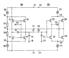
- Circuit tampon de sortie comprenant un premier circuit inverseur avec une borne d'entrée et une borne de sortie, qui constituent également la borne d'entrée et la borne de sortie du circuit tampon, et avec des bornes pour une première tension d'alimentation, un montage en série d'un deuxième circuit inverseur et d'un premier condensateur étant inséré entre la borne d'entrée et la borne de sortie du circuit tampon, lequel deuxième circuit inverseur est connecté à des bornes pour une deuxième tension d'alimentation, caractérisé en ce que l'amplitude crête-crête de tension du signal de sortie à la borne de sortie du circuit tampon est une fraction prédéterminée de l'amplitude crête-crête du signal appliqué à la borne d'entrée, et en ce que des moyens de détermination sont prévus pour déterminer un niveau de tension de référence comme signal de sortie supplémentaire, lesdits moyens de détermination recevant la première tension d'alimentation.
- Circuit tampon suivant la revendication 1, dans lequel les première et deuxième tensions d'alimentation sont des tensions d'alimentation symétriques, caractérisé en ce que le premier circuit inverseur comprend au moins une paire complémentaire de transistors à effet de champ dont respectivement les connexions de grille et de drain sont mutuellement couplées, dans laquelle la borne d'entrée est couplée aux connexions de grille mutuellement couplées et la borne de sortie est couplée aux connexions de drain mutuellement couplées, dans laquelle la connexion de source du FET à canal p de la paire complémentaire est couplée à la borne pour la première tension d'alimentation positive et la connexion de source du FET à canal n de la paire est couplée à la borne pour la première tension d'alimentation négative, et en ce que le niveau de tension de référence se situe entre les deuxièmes niveaux positif et négatif de tension.
- Circuit tampon pour un circuit tampon suivant la revendication 1 ou 2 et comprenant un troisième circuit inverseur avec une borne d'entrée et une borne de sortie, qui constituent également les bornes d'entrée et de sortie du circuit tampon, et couplées à des bornes pour la deuxième tension d'alimentation, le troisième circuit inverseur comprenant un inverseur CMOS et présentant à la borne de sortie une version agrandie de l'amplitude crête-crête de tension du signal reçu à la borne d'entrée, et une deuxième borne d'entrée recevant ledit niveau de tension de référence et le fournissant à des moyens destinés à réduire la tension de décalage du circuit tampon, ledit moyen de réduction étant connecté entre les bornes d'alimentation dudit troisième inverseur.
- Circuit tampon suivant la revendication 3, caractérisé en ce que le moyen de réduction destiné à réduire la tension de décalage du circuit tampon comprend une autre paire de FET complémentaires, dans laquelle chacun de ces FET a ses connexions de grille et de drain mutuellement couplées et ces connexions mutuellement couplées des deux FET sont couplées à la deuxième borne d'entrée et dans laquelle les connexions de source des deux FET sont couplées à la connexion de source du FET correspondant de la paire complémentaire.
- Circuit tampon suivant la revendication 3 ou 4, caractérisé en ce que l'amplitude crête-crête de tension du signal à la borne de sortie est la même que celle du signal à la borne de sortie du circuit tampon de sortie.
- Système comprenant un circuit tampon fonctionnant comme circuit tampon de sortie suivant la revendication 1 ou 2, dont la sortie est couplée à l'entrée d'un circuit tampon fonctionnant comme circuit tampon d'entrée suivant la revendication 3, 4 ou 5, caractérisé en ce que, entre la borne de sortie du circuit tampon de sortie et un niveau commun de tension et entre la borne d'entrée du circuit tampon d'entrée et ce niveau commun de tension, respectivement un deuxième et un troisième condensateurs sont fournis, qui, en combinaison avec le premier condensateur, constituent un diviseur de tension capacitif.
- Circuit tampon suivant l'une quelconque des revendications 1 à 4, caractérisé en ce que tous les FET sont agencés comme des C-MOSFET.
- Circuit tampon suivant l'une quelconque des revendications 1 à 4, caractérisé en ce que les premiers niveaux de tension d'alimentation sont respectivement de +250 mV et -250 mV et en ce que les deuxièmes niveaux de tension d'alimentation sont respectivement de +5 volts et -5 volts.
Priority Applications (1)
| Application Number | Priority Date | Filing Date | Title |
|---|---|---|---|
| EP93201982A EP0579314B1 (fr) | 1992-07-14 | 1993-07-07 | Ensemble constitué par des circuits tampons d'entrée et de sortie |
Applications Claiming Priority (3)
| Application Number | Priority Date | Filing Date | Title |
|---|---|---|---|
| EP92202152 | 1992-07-14 | ||
| EP92202152 | 1992-07-14 | ||
| EP93201982A EP0579314B1 (fr) | 1992-07-14 | 1993-07-07 | Ensemble constitué par des circuits tampons d'entrée et de sortie |
Publications (2)
| Publication Number | Publication Date |
|---|---|
| EP0579314A1 EP0579314A1 (fr) | 1994-01-19 |
| EP0579314B1 true EP0579314B1 (fr) | 1998-04-29 |
Family
ID=26131558
Family Applications (1)
| Application Number | Title | Priority Date | Filing Date |
|---|---|---|---|
| EP93201982A Expired - Lifetime EP0579314B1 (fr) | 1992-07-14 | 1993-07-07 | Ensemble constitué par des circuits tampons d'entrée et de sortie |
Country Status (1)
| Country | Link |
|---|---|
| EP (1) | EP0579314B1 (fr) |
Families Citing this family (4)
| Publication number | Priority date | Publication date | Assignee | Title |
|---|---|---|---|---|
| GB9508886D0 (en) * | 1995-05-02 | 1995-06-21 | Plessey Semiconductors Ltd | Integrated circuit output buffer |
| SE509882C2 (sv) * | 1995-11-10 | 1999-03-15 | Ericsson Telefon Ab L M | Mottagarkrets innefattande parallella ingångskretsar |
| US7538633B2 (en) * | 2004-09-28 | 2009-05-26 | Sun Microsystems, Inc. | Method and apparatus for driving on-chip wires through capacitive coupling |
| CN110708056B (zh) * | 2019-10-11 | 2023-01-17 | 湖南国科微电子股份有限公司 | 一种输入缓冲电路和输入缓冲方法 |
Family Cites Families (2)
| Publication number | Priority date | Publication date | Assignee | Title |
|---|---|---|---|---|
| DE2346966B2 (de) * | 1973-09-18 | 1976-07-29 | Siemens AG, 1000 Berlin und 8000 München | Verfahren zur uebertragung von signalen zwischen zwei chips mit schnellen komplementaer-mos-schaltungen |
| JPS5516539A (en) * | 1978-07-20 | 1980-02-05 | Nec Corp | Level shifter circuit |
-
1993
- 1993-07-07 EP EP93201982A patent/EP0579314B1/fr not_active Expired - Lifetime
Also Published As
| Publication number | Publication date |
|---|---|
| EP0579314A1 (fr) | 1994-01-19 |
Similar Documents
| Publication | Publication Date | Title |
|---|---|---|
| US4841175A (en) | ECL-compatible input/output circuits in CMOS technology | |
| US5864587A (en) | Differential signal receiver | |
| US5140179A (en) | Master-slave type flip-flop circuit | |
| US4866301A (en) | Controlled slew peak detector | |
| US4794283A (en) | Edge sensitive level translating and rereferencing CMOS circuitry | |
| US5397940A (en) | Buffer system with reduced interference | |
| US4581545A (en) | Schmitt trigger circuit | |
| US4656372A (en) | CMOS to ECL interface circuit | |
| EP0194134B1 (fr) | Circuit intégré à semi-conducteur | |
| US6515532B2 (en) | Level shift circuit for shifting voltage levels | |
| JPH06224733A (ja) | 送受信回路およびそのための方法 | |
| EP0851434B1 (fr) | Circuit échantillonneur-bloqueur et dispositif à semi-conducteurs le comportant | |
| US4794276A (en) | Latch circuit tolerant of undefined control signals | |
| US7230469B2 (en) | Multi-level/single ended input level shifter circuit | |
| EP0579314B1 (fr) | Ensemble constitué par des circuits tampons d'entrée et de sortie | |
| US5666068A (en) | GTL input receiver with hysteresis | |
| US6501401B2 (en) | Means for compensating a data-dependent supply current in an electronic circuit | |
| US5644262A (en) | Digitally controlled capacitive load | |
| US7157931B2 (en) | Termination circuits having pull-down and pull-up circuits and related methods | |
| US5748024A (en) | Level convertor | |
| US4810912A (en) | Current switch | |
| JP2001111419A (ja) | チャージポンプ回路 | |
| US5105106A (en) | Circuit configuration for converting TTL-level signals into CML or ECL-level signals | |
| JPH1079659A (ja) | 半導体集積回路装置 | |
| JPH01279623A (ja) | インターフェイス回路 |
Legal Events
| Date | Code | Title | Description |
|---|---|---|---|
| PUAI | Public reference made under article 153(3) epc to a published international application that has entered the european phase |
Free format text: ORIGINAL CODE: 0009012 |
|
| AK | Designated contracting states |
Kind code of ref document: A1 Designated state(s): DE FR GB IT SE |
|
| 17P | Request for examination filed |
Effective date: 19940629 |
|
| RAP1 | Party data changed (applicant data changed or rights of an application transferred) |
Owner name: N.V. PHILIPS' GLOEILAMPENFABRIEKEN |
|
| 17Q | First examination report despatched |
Effective date: 19960617 |
|
| GRAG | Despatch of communication of intention to grant |
Free format text: ORIGINAL CODE: EPIDOS AGRA |
|
| GRAG | Despatch of communication of intention to grant |
Free format text: ORIGINAL CODE: EPIDOS AGRA |
|
| GRAH | Despatch of communication of intention to grant a patent |
Free format text: ORIGINAL CODE: EPIDOS IGRA |
|
| GRAH | Despatch of communication of intention to grant a patent |
Free format text: ORIGINAL CODE: EPIDOS IGRA |
|
| GRAA | (expected) grant |
Free format text: ORIGINAL CODE: 0009210 |
|
| RAP1 | Party data changed (applicant data changed or rights of an application transferred) |
Owner name: PHILIPS ELECTRONICS N.V. |
|
| AK | Designated contracting states |
Kind code of ref document: B1 Designated state(s): DE FR GB IT SE |
|
| REF | Corresponds to: |
Ref document number: 69318222 Country of ref document: DE Date of ref document: 19980604 |
|
| ITF | It: translation for a ep patent filed |
Owner name: ING. C. GREGORJ S.P.A. |
|
| ET | Fr: translation filed | ||
| RAP4 | Party data changed (patent owner data changed or rights of a patent transferred) |
Owner name: KONINKLIJKE PHILIPS ELECTRONICS N.V. |
|
| REG | Reference to a national code |
Ref country code: FR Ref legal event code: CD |
|
| PLBE | No opposition filed within time limit |
Free format text: ORIGINAL CODE: 0009261 |
|
| STAA | Information on the status of an ep patent application or granted ep patent |
Free format text: STATUS: NO OPPOSITION FILED WITHIN TIME LIMIT |
|
| 26N | No opposition filed | ||
| PGFP | Annual fee paid to national office [announced via postgrant information from national office to epo] |
Ref country code: SE Payment date: 20010726 Year of fee payment: 9 |
|
| REG | Reference to a national code |
Ref country code: GB Ref legal event code: IF02 |
|
| PG25 | Lapsed in a contracting state [announced via postgrant information from national office to epo] |
Ref country code: SE Free format text: LAPSE BECAUSE OF NON-PAYMENT OF DUE FEES Effective date: 20020708 |
|
| REG | Reference to a national code |
Ref country code: FR Ref legal event code: D6 |
|
| REG | Reference to a national code |
Ref country code: GB Ref legal event code: 746 Effective date: 20021209 |
|
| EUG | Se: european patent has lapsed | ||
| PGFP | Annual fee paid to national office [announced via postgrant information from national office to epo] |
Ref country code: FR Payment date: 20030729 Year of fee payment: 11 |
|
| PGFP | Annual fee paid to national office [announced via postgrant information from national office to epo] |
Ref country code: GB Payment date: 20030730 Year of fee payment: 11 |
|
| PGFP | Annual fee paid to national office [announced via postgrant information from national office to epo] |
Ref country code: DE Payment date: 20030916 Year of fee payment: 11 |
|
| PG25 | Lapsed in a contracting state [announced via postgrant information from national office to epo] |
Ref country code: GB Free format text: LAPSE BECAUSE OF NON-PAYMENT OF DUE FEES Effective date: 20040707 |
|
| PG25 | Lapsed in a contracting state [announced via postgrant information from national office to epo] |
Ref country code: DE Free format text: LAPSE BECAUSE OF NON-PAYMENT OF DUE FEES Effective date: 20050201 |
|
| GBPC | Gb: european patent ceased through non-payment of renewal fee |
Effective date: 20040707 |
|
| PG25 | Lapsed in a contracting state [announced via postgrant information from national office to epo] |
Ref country code: FR Free format text: LAPSE BECAUSE OF NON-PAYMENT OF DUE FEES Effective date: 20050331 |
|
| REG | Reference to a national code |
Ref country code: FR Ref legal event code: ST |
|
| PG25 | Lapsed in a contracting state [announced via postgrant information from national office to epo] |
Ref country code: IT Free format text: LAPSE BECAUSE OF NON-PAYMENT OF DUE FEES Effective date: 20050707 |