EP0579314B1 - System comprising an output buffer circuit and an input buffer circuit - Google Patents
System comprising an output buffer circuit and an input buffer circuit Download PDFInfo
- Publication number
- EP0579314B1 EP0579314B1 EP93201982A EP93201982A EP0579314B1 EP 0579314 B1 EP0579314 B1 EP 0579314B1 EP 93201982 A EP93201982 A EP 93201982A EP 93201982 A EP93201982 A EP 93201982A EP 0579314 B1 EP0579314 B1 EP 0579314B1
- Authority
- EP
- European Patent Office
- Prior art keywords
- buffer circuit
- output
- voltage
- coupled
- terminal
- Prior art date
- Legal status (The legal status is an assumption and is not a legal conclusion. Google has not performed a legal analysis and makes no representation as to the accuracy of the status listed.)
- Expired - Lifetime
Links
Images
Classifications
-
- H—ELECTRICITY
- H03—ELECTRONIC CIRCUITRY
- H03K—PULSE TECHNIQUE
- H03K19/00—Logic circuits, i.e. having at least two inputs acting on one output; Inverting circuits
- H03K19/003—Modifications for increasing the reliability for protection
- H03K19/00346—Modifications for eliminating interference or parasitic voltages or currents
- H03K19/00361—Modifications for eliminating interference or parasitic voltages or currents in field effect transistor circuits
-
- H—ELECTRICITY
- H03—ELECTRONIC CIRCUITRY
- H03K—PULSE TECHNIQUE
- H03K19/00—Logic circuits, i.e. having at least two inputs acting on one output; Inverting circuits
- H03K19/0175—Coupling arrangements; Interface arrangements
- H03K19/0185—Coupling arrangements; Interface arrangements using field effect transistors only
- H03K19/018507—Interface arrangements
- H03K19/018521—Interface arrangements of complementary type, e.g. CMOS
Definitions
- the invention relates to a buffer circuit, more specifically, an output buffer circuit comprising a first inverter circuit with an input terminal and an output terminal which also form the input terminal and the output terminal of the buffer circuit, and with terminals for a first supply voltage, there being inserted between the input terminal and the output terminal of the buffer circuit a series combination of a second inverter circuit and a first capacitor which second inverter circuit is connected to terminals for a second supply voltage.
- the first inverter circuit comprises at least a complementary pair of field effect transistors whose gate and drain connections are mutually coupled, in which the input terminal is coupled to the mutually coupled gate connections and the output terminal is coupled to the mutually coupled drain connections, in which the source connection of the p-channel FET of the complementary pair is coupled to the terminal for the first positive supply voltage and the source connection of the n-channel FET of the pair is coupled to the terminal for the first negative supply voltage.
- a buffer circuit of this type is known from DE-A-2929450 in the form of a level shifter.
- This known circuit has for its object to convert an input voltage level into another, higher output voltage level while the output of the circuit comprising C-MOSFET's is capable of rapidly following voltage changes on the input.
- an inverter connected to the input terminal is provided, whose output terminal is connected to the output terminal of the buffer circuit via a capacitor combined in series with the output terminal.
- the inverter is coupled, on one side, to the positive supply voltage terminal and, on the other side, to a connection for a negative supply voltage which is less negative than the negative supply voltage for the complementary pair of FET's.
- the combination of the inverter and the capacitor which forms a differentiator, transfers very rapidly input voltage variations with a limited voltage swing to the output of the circuit, while the final output voltage level is reached in a conventional manner when one of the FET's conducts in an, of necessity, slightly delayed manner.
- the switch delay occurring in a thus structured circuit of C-MOSFET's is distinctly smaller than in a circuit comprising exclusively C-MOSFETS.
- a disadvantage of the prior art circuit is that the voltage swing at the output is determined, on one hand, by the positive voltage level and, on the other hand, by the most negative voltage level so that, as a result of the high peak currents flowing through the supply lines during voltage transitions, annoying disturbing signals occur everywhere in the circuit that comprises the buffer circuit.
- the invention thereto provides a buffer circuit of said type, characterised in that the voltage swing of the output signal on the output terminal of the buffer circuit is a predetermined fraction of the voltage swing of the signal applied to the input terminal and in that determining means are provided for determining a reference voltage level as a further output signal, said determining means receiving the first supply voltage.
- the invention is based on the recognition that the problems occurring due to the high peak currents during the change of the output voltage level may largely be suppressed, on one hand, by determining the output voltage of the buffer circuit at a considerably lower level in lieu of the customary TTL-compatible level of 5 volts, so that also the occurring peak currents are considerably smaller as a result of the much smaller voltage swing in the output signal determined by the maximum drive of the first inverter circuit and, on the other hand, by defining a reference voltage level situated between the two extreme voltage levels of the buffer circuit output voltage, while the line carrying this reference voltage does not conduct signal currents and is therefore largely free from disturbing signals, so that there is avoided that the relatively low output voltage level is affected by disturbing signals.
- the output of the buffer circuit can be transferred to another circuit, for example, another IC which is then capable of reconstructing from these two signals the input signal of the buffer circuit in the other circuit.
- the invention likewise relates to an input buffer circuit which is capable of performing this operation, this buffer circuit comprising a third inverter circuit with an input terminal and an output terminal which also form the input and output terminals of the buffer circuit, and with terminals for the second supply voltage and which is characterised, in that the third inverter circuit amplifies the signal received on the input terminal, by a second input terminal for receiving the reference voltage level and by reducing means for reducing the offset voltage of the buffer circuit and in that the third inverter circuit comprises at least a complementary pair of field effect transistors, whose respective gate and drain connections are mutually coupled, in which the input terminal is coupled to the mutually coupled gate connections and the output terminal is coupled to the mutually coupled drain connections, in which the source connection of the p-channel FET of the complementary pair is coupled to the terminal for the second positive supply voltage and the source connection of the n-channel FET of the pair is coupled to the terminal for the second negative supply voltage.
- this buffer circuit comprising a third inverter circuit with an input terminal and an output terminal which
- the complementary pair of FET's restores the input voltage up to the original voltage level having a 5-volt swing
- the reducing means for reducing the offset voltage preferably comprising a further pair of complementary FET's, each one of these FET's having its gate and drain connections coupled and these mutually coupled connections of the two FET's being coupled to the second input terminal and the source connections of the two FET's being coupled to the source connection of the corresponding FET of the complementary pair. This measure limits the offset voltage of the input buffer circuit.
- the inverter and the capacitor directly transfer to the output of the output buffer circuit, so that it does not exceed the output voltage of the buffer circuit itself which is undesired because it leads to signal distortion of the output signal in the form of overshoot, preferably between the output terminal of the output buffer circuit and a common voltage level (earth) and between the input terminal of the input buffer circuit and this common voltage level, preferably a second and a third capacitor respectively, are provided which, in combination with the first capacitor, constitute a capacitive voltage divider for reducing the input voltage swing of the output buffer circuit to a maximum of the output voltage swing thereof.
- the two buffer circuits may be present, for example, in two separate integrated circuits, between which pulse-shaped (logic) signals are to be transmitted.
- Such integrated circuits may, for example, form part of an echo canceller for telephony purposes in which one IC comprises the analog interface to the telephone line and the other IC the digital circuit for the signal processing.
- a clock signal having a frequency of, for example, 7.68 MHz, a sign signal having a frequency of, for example, 80 kHZ, as well as the output signal of an analog-to-digital converter, for example, a sigma delta modulator, are then transmitted between such ICs.
- one IC could then comprise a output buffer circuit according to the invention and the other IC an input buffer circuit according to the invention.
- the buffer circuits according to the invention may also be applied to many other types of circuits than those used for telephony.
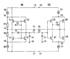
- the output buffer circuit 100 comprises a first inverter circuit preferably formed by an n-channel C-MOSFET 101 and a p-channel C-MOSFET 102, together forming a complementary pair, in which the gate and drain connections respectively, of the FET's are mutually coupled.
- An input terminal 103 of the output buffer circuit is coupled to the mutually coupled gate connections and an output terminal 117 is coupled to the mutually coupled drain connections.
- the source connection of the FET 102 is coupled to a junction 104 for a first positive supply voltage and the source connection of the FET 101 is coupled to a junction 105 for a first negative supply voltage.
- the voltage level at the junctions 104 and 105 determines the maximum voltage swing of the output buffer circuit output voltage on terminal 117 and this swing, according to the exemplary embodiment, is ten times smaller than the swing of the voltage applied to the input 103.
- the output voltage thus has a voltage swing of 0.5 volt which means that the supply voltage on the respective terminals 104 and 105 is to be +250 mV and -250 mV for the first inverter circuit.
- the positive voltage level is determined in a manner known per se by means of a series combination of a current source 106 and a resistor 107 which combination is inserted between the terminal 110 for a second positive supply voltage of, for example, +2.5 volts, and a reference voltage line 112.
- the voltage level of +250 mV is then available at the junction between the current source 106 and the resistor 107 when the current supplied by the current source and the magnitude of the resistor are properly chosen.
- the negative first supply voltage at junction 105 is determined by a current source 108 and a resistor 109, the current source 108 being connected to a terminal 111 for a second negative supply voltage of, for example, -2.5 volts.
- the voltage level on line 112 is equal to 0 volts.
- the voltage level on the output terminal 117 is not related, as is customary in the state of the art, to one of the supply voltage levels on the line 110 or 111 and neither is it related to the voltage level on the terminal 118 for the common voltage level (earth), in order to prevent that the, though low, but still present disturbing signals on these lines detrimentally affect the now relatively low output voltage level.
- the output voltage is related to the reference voltage level on line 112 through which line no signal currents flow any longer, so that this reference voltage is very "pure".
- the buffer circuit 100 comprises a second inverter circuit, preferably also constituted by C-MOSFET's, i. e . an n-channel C-MOSFET 113 and a p-channel C-MOSFET 114, together forming a complementary pair in which the gate and drain connections of the FET's are mutually coupled.
- the source connections of the FET's 113 and 114 are connected to the second negative supply voltage level of -2.5 volts on line 111 and the second positive supply voltage level of +2.5 volts on line 110 respectively.
- the mutually coupled gate connections are connected to the input terminal 103 and the mutually coupled drain connections are connected to the output terminal 117 by way of a capacitor 115.
- a capacitor 115 With this combination of an inverter circuit and a capacitor, input voltage variations may be transferred rapidly to the output so as to enhance the edge steepness of the output voltage.
- the inverter circuit comprising the FET's 113 and 114 to transfer the complete voltage swing of 5 volts to the output 117 by way of the capacitor 115, because this may lead to overshoot in the output signal. Therefore, a second capacitor 119 is provided which is connected to the output terminal 117 and to the common voltage level at point 118 and which, together with the capacitor 115, forms a capacitive voltage divider limiting the voltage swing on output 117.
- the output buffer circuit 200 comprises voltage supply terminals 215, 210 and 211 which carry the same supply voltage levels as the respective lines 118, 110 and 111 in the output buffer circuit 100 and which, according to the embodiment, thus carry the common voltage levels (earth) of +2.5 volts and -2.5 volts respectively.
- the input buffer circuit 200 further includes an inverter circuit comprising an n-channel C-MOSFET 201 and a p-channel C-MOSFET 202 which together form a complementary pair in which the gate and drain connections of the FET's are mutually coupled.
- the input terminal 203 of the input buffer circuit is coupled to the mutually coupled gate connections and an output terminal 204 is coupled to the mutually coupled drain connections.
- the source connection of the FET 202 is coupled to a terminal 206 of a current source 212 which is supplied from the positive supply voltage line 210 and the source connection of the FET 201 is coupled to a terminal 207 of a current source 213 which is supplied from the negative supply voltage line 211.
- the FET's 201 and 202 may thus reconvert an input voltage having a 0.5-volt swing received from the output terminal 117 of the output buffer circuit 100 into an inverted output voltage having a 5-volt swing on the output terminal 204, so that the signal on the input 103 of circuit 100 is again available with the right polarity and voltage swing at the output 204 of circuit 200.
- a n-channel C-MOSFET 208 and a p-channel C-MOSFET 209 which together form a complementary pair in which the gate and drain connections of these two FET's 210 and 209 are mutually coupled and are also connected to a terminal 205 for receiving the reference voltage level from terminal 116 of the circuit 100.
- the source connection of the n-channel C-MOSFET 208 is also connected to the terminal 207 of the current source 213 and the source connection of the p-channel C-MOSFET 209 is connected to the terminal 206 of the current source 212.
- the offset voltage may be reduced to a negligibly small level.
- a capacitor 214 is inserted which, in combination with the capacitor 119 of circuit 100, determines the divisor of the capacitive voltage divider.
- the values of the capacitors 119 and 214 are computed, the magnitude of the already available (parasitic) output capacitance or input capacitance respectively, of the circuits 100 and 200 may be taken into account.
Description
Claims (8)
- An output buffer circuit comprising a first inverter circuit with an input terminal and an output terminal which also form the input terminal and the output terminal of the buffer circuit, and with terminals for a first supply voltage, there being inserted between the input terminal and the output terminal of the buffer circuit a series combination of a second inverter circuit and a first capacitor which second inverter circuit is connected to terminals for a second supply voltage, characterised in that the voltage swing of the output signal on the output terminal of the buffer circuit is a predetermined fraction of the voltage swing of the signal applied to the input terminal and in that determining means are provided for determining a reference voltage level as a further output signal, said determining means receiving the first supply voltage.
- Buffer circuit as claimed in Claim 1, in which the first and second supply voltages are symmetrical supply voltages, characterised in that the first inverter circuit comprises at least a complementary pair of field effect transistors whose gate and drain connections respectively, are mutually coupled, in which the input terminal is coupled to the mutually coupled gate connections and the output terminal is coupled to the mutually coupled drain connections, in which the source connection of the p-channel FET of the complementary pair is coupled to the terminal for the first positive supply voltage and the source connection of the n-channel FET of the pair is coupled to the terminal for the first negative supply voltage and in that the reference voltage level is situated between the positive and the negative second voltage level.
- Buffer circuit for a buffer circuit as claimed in Claim 1 or 2 and comprising a third inverter circuit with an input terminal and an output terminal which also form the input and output terminals of the buffer circuit, and coupled to terminals for the second supply voltage, whereby the third inverter comprises a CMOS inverter and presents on the output terminal an enlarged version of the voltage swing of the signal received on the input terminal, and whereby a second input terminal receives said reference voltage level and provides it to means for reducing the offset voltage of the buffer circuit, said reducing means being connected between the power supply terminals of said third inverter.
- Buffer circuit as claimed in Claim 3, characterised in that the reducing means for reducing the offset voltage of the buffer circuit comprises a further pair of complementary FET's, in which each one of these FET's has its gate and drain connections mutually coupled and these mutually coupled connections of the two FET's are coupled to the second input terminal and in which the source connections of the two FET's are coupled to the source connection of the corresponding FET of the complementary pair.
- Buffer circuit as claimed in one of the Claims 3 or 4, characterised in that the voltage swing of the signal on the output terminal is the same as that of the signal on the output terminal of the output buffer circuit.
- System comprising a buffer circuit operating as an output buffer circuit as claimed in Claim 1 or 2, whose output is coupled to the input of a buffer circuit operating as an input buffer circuit as claimed in Claim 3, 4 or 5, characterised in that between the output terminal of the output buffer circuit and a common voltage level and between the input terminal of the input buffer circuit and this common voltage level a second and a third capacitor respectively, are provided which, in combination with the first capacitor, constitute a capacitive voltage divider.
- Buffer circuit as claimed in one of the Claims 1 to 4, characterised in that all the FET's are arranged as C-MOSFET's.
- Buffer circuit as claimed in one of the Claims 1 to 4, characterized in that the first supply voltage level is +250 mV and -250 mV respectively, and in that the second supply voltage level is +5 volts and -5 volts respectively.
Priority Applications (1)
| Application Number | Priority Date | Filing Date | Title |
|---|---|---|---|
| EP93201982A EP0579314B1 (en) | 1992-07-14 | 1993-07-07 | System comprising an output buffer circuit and an input buffer circuit |
Applications Claiming Priority (3)
| Application Number | Priority Date | Filing Date | Title |
|---|---|---|---|
| EP92202152 | 1992-07-14 | ||
| EP92202152 | 1992-07-14 | ||
| EP93201982A EP0579314B1 (en) | 1992-07-14 | 1993-07-07 | System comprising an output buffer circuit and an input buffer circuit |
Publications (2)
| Publication Number | Publication Date |
|---|---|
| EP0579314A1 EP0579314A1 (en) | 1994-01-19 |
| EP0579314B1 true EP0579314B1 (en) | 1998-04-29 |
Family
ID=26131558
Family Applications (1)
| Application Number | Title | Priority Date | Filing Date |
|---|---|---|---|
| EP93201982A Expired - Lifetime EP0579314B1 (en) | 1992-07-14 | 1993-07-07 | System comprising an output buffer circuit and an input buffer circuit |
Country Status (1)
| Country | Link |
|---|---|
| EP (1) | EP0579314B1 (en) |
Families Citing this family (4)
| Publication number | Priority date | Publication date | Assignee | Title |
|---|---|---|---|---|
| GB9508886D0 (en) * | 1995-05-02 | 1995-06-21 | Plessey Semiconductors Ltd | Integrated circuit output buffer |
| SE509882C2 (en) * | 1995-11-10 | 1999-03-15 | Ericsson Telefon Ab L M | Receiver circuit comprising parallel input circuits |
| US7538633B2 (en) | 2004-09-28 | 2009-05-26 | Sun Microsystems, Inc. | Method and apparatus for driving on-chip wires through capacitive coupling |
| CN110708056B (en) * | 2019-10-11 | 2023-01-17 | 湖南国科微电子股份有限公司 | Input buffer circuit and input buffer method |
Family Cites Families (2)
| Publication number | Priority date | Publication date | Assignee | Title |
|---|---|---|---|---|
| DE2346966B2 (en) * | 1973-09-18 | 1976-07-29 | Siemens AG, 1000 Berlin und 8000 München | METHOD OF TRANSFERRING SIGNALS BETWEEN TWO CHIPS WITH FAST COMPLEMENTARY MOS CIRCUITS |
| JPS5516539A (en) * | 1978-07-20 | 1980-02-05 | Nec Corp | Level shifter circuit |
-
1993
- 1993-07-07 EP EP93201982A patent/EP0579314B1/en not_active Expired - Lifetime
Also Published As
| Publication number | Publication date |
|---|---|
| EP0579314A1 (en) | 1994-01-19 |
Similar Documents
| Publication | Publication Date | Title |
|---|---|---|
| US4841175A (en) | ECL-compatible input/output circuits in CMOS technology | |
| US5864587A (en) | Differential signal receiver | |
| US5140179A (en) | Master-slave type flip-flop circuit | |
| US4866301A (en) | Controlled slew peak detector | |
| US4794283A (en) | Edge sensitive level translating and rereferencing CMOS circuitry | |
| US5397940A (en) | Buffer system with reduced interference | |
| US4656372A (en) | CMOS to ECL interface circuit | |
| EP0194134B1 (en) | Semiconductor integrated circuit device | |
| US6515532B2 (en) | Level shift circuit for shifting voltage levels | |
| JPH06224733A (en) | Transmission and reception circuits, and method therefor | |
| EP0851434B1 (en) | Sample hold circuit and semiconductor device having the same | |
| US4794276A (en) | Latch circuit tolerant of undefined control signals | |
| US7230469B2 (en) | Multi-level/single ended input level shifter circuit | |
| EP0579314B1 (en) | System comprising an output buffer circuit and an input buffer circuit | |
| US5666068A (en) | GTL input receiver with hysteresis | |
| US6501401B2 (en) | Means for compensating a data-dependent supply current in an electronic circuit | |
| US5644262A (en) | Digitally controlled capacitive load | |
| US7157931B2 (en) | Termination circuits having pull-down and pull-up circuits and related methods | |
| KR20010023574A (en) | Data transmission device | |
| US5748024A (en) | Level convertor | |
| US4810912A (en) | Current switch | |
| US6366126B1 (en) | Input circuit, output circuit, and input/output circuit and signal transmission system using the same input/output circuit | |
| US5287517A (en) | Self-compensating voltage level shifting circuit | |
| JP2001111419A (en) | Charge pump circuit | |
| US5105106A (en) | Circuit configuration for converting TTL-level signals into CML or ECL-level signals |
Legal Events
| Date | Code | Title | Description |
|---|---|---|---|
| PUAI | Public reference made under article 153(3) epc to a published international application that has entered the european phase |
Free format text: ORIGINAL CODE: 0009012 |
|
| AK | Designated contracting states |
Kind code of ref document: A1 Designated state(s): DE FR GB IT SE |
|
| 17P | Request for examination filed |
Effective date: 19940629 |
|
| RAP1 | Party data changed (applicant data changed or rights of an application transferred) |
Owner name: N.V. PHILIPS' GLOEILAMPENFABRIEKEN |
|
| 17Q | First examination report despatched |
Effective date: 19960617 |
|
| GRAG | Despatch of communication of intention to grant |
Free format text: ORIGINAL CODE: EPIDOS AGRA |
|
| GRAG | Despatch of communication of intention to grant |
Free format text: ORIGINAL CODE: EPIDOS AGRA |
|
| GRAH | Despatch of communication of intention to grant a patent |
Free format text: ORIGINAL CODE: EPIDOS IGRA |
|
| GRAH | Despatch of communication of intention to grant a patent |
Free format text: ORIGINAL CODE: EPIDOS IGRA |
|
| GRAA | (expected) grant |
Free format text: ORIGINAL CODE: 0009210 |
|
| RAP1 | Party data changed (applicant data changed or rights of an application transferred) |
Owner name: PHILIPS ELECTRONICS N.V. |
|
| AK | Designated contracting states |
Kind code of ref document: B1 Designated state(s): DE FR GB IT SE |
|
| REF | Corresponds to: |
Ref document number: 69318222 Country of ref document: DE Date of ref document: 19980604 |
|
| ITF | It: translation for a ep patent filed |
Owner name: ING. C. GREGORJ S.P.A. |
|
| ET | Fr: translation filed | ||
| RAP4 | Party data changed (patent owner data changed or rights of a patent transferred) |
Owner name: KONINKLIJKE PHILIPS ELECTRONICS N.V. |
|
| REG | Reference to a national code |
Ref country code: FR Ref legal event code: CD |
|
| PLBE | No opposition filed within time limit |
Free format text: ORIGINAL CODE: 0009261 |
|
| STAA | Information on the status of an ep patent application or granted ep patent |
Free format text: STATUS: NO OPPOSITION FILED WITHIN TIME LIMIT |
|
| 26N | No opposition filed | ||
| PGFP | Annual fee paid to national office [announced via postgrant information from national office to epo] |
Ref country code: SE Payment date: 20010726 Year of fee payment: 9 |
|
| REG | Reference to a national code |
Ref country code: GB Ref legal event code: IF02 |
|
| PG25 | Lapsed in a contracting state [announced via postgrant information from national office to epo] |
Ref country code: SE Free format text: LAPSE BECAUSE OF NON-PAYMENT OF DUE FEES Effective date: 20020708 |
|
| REG | Reference to a national code |
Ref country code: FR Ref legal event code: D6 |
|
| REG | Reference to a national code |
Ref country code: GB Ref legal event code: 746 Effective date: 20021209 |
|
| EUG | Se: european patent has lapsed | ||
| PGFP | Annual fee paid to national office [announced via postgrant information from national office to epo] |
Ref country code: FR Payment date: 20030729 Year of fee payment: 11 |
|
| PGFP | Annual fee paid to national office [announced via postgrant information from national office to epo] |
Ref country code: GB Payment date: 20030730 Year of fee payment: 11 |
|
| PGFP | Annual fee paid to national office [announced via postgrant information from national office to epo] |
Ref country code: DE Payment date: 20030916 Year of fee payment: 11 |
|
| PG25 | Lapsed in a contracting state [announced via postgrant information from national office to epo] |
Ref country code: GB Free format text: LAPSE BECAUSE OF NON-PAYMENT OF DUE FEES Effective date: 20040707 |
|
| PG25 | Lapsed in a contracting state [announced via postgrant information from national office to epo] |
Ref country code: DE Free format text: LAPSE BECAUSE OF NON-PAYMENT OF DUE FEES Effective date: 20050201 |
|
| GBPC | Gb: european patent ceased through non-payment of renewal fee |
Effective date: 20040707 |
|
| PG25 | Lapsed in a contracting state [announced via postgrant information from national office to epo] |
Ref country code: FR Free format text: LAPSE BECAUSE OF NON-PAYMENT OF DUE FEES Effective date: 20050331 |
|
| REG | Reference to a national code |
Ref country code: FR Ref legal event code: ST |
|
| PG25 | Lapsed in a contracting state [announced via postgrant information from national office to epo] |
Ref country code: IT Free format text: LAPSE BECAUSE OF NON-PAYMENT OF DUE FEES Effective date: 20050707 |