EP0577998B1 - Field effect transistor - Google Patents
Field effect transistor Download PDFInfo
- Publication number
- EP0577998B1 EP0577998B1 EP93109418A EP93109418A EP0577998B1 EP 0577998 B1 EP0577998 B1 EP 0577998B1 EP 93109418 A EP93109418 A EP 93109418A EP 93109418 A EP93109418 A EP 93109418A EP 0577998 B1 EP0577998 B1 EP 0577998B1
- Authority
- EP
- European Patent Office
- Prior art keywords
- effect transistor
- field effect
- common
- gates
- drain region
- Prior art date
- Legal status (The legal status is an assumption and is not a legal conclusion. Google has not performed a legal analysis and makes no representation as to the accuracy of the status listed.)
- Expired - Lifetime
Links
- 230000005669 field effect Effects 0.000 title claims description 12
- 230000005611 electricity Effects 0.000 description 3
- 238000011161 development Methods 0.000 description 2
- 230000018109 developmental process Effects 0.000 description 2
- 238000013528 artificial neural network Methods 0.000 description 1
- 239000004020 conductor Substances 0.000 description 1
- 239000003669 enzymatically hydrolysed carboxymethyl cellulose Substances 0.000 description 1
Images

Classifications
-
- H—ELECTRICITY
- H10—SEMICONDUCTOR DEVICES; ELECTRIC SOLID-STATE DEVICES NOT OTHERWISE PROVIDED FOR
- H10D—INORGANIC ELECTRIC SEMICONDUCTOR DEVICES
- H10D30/00—Field-effect transistors [FET]
- H10D30/60—Insulated-gate field-effect transistors [IGFET]
- H10D30/611—Insulated-gate field-effect transistors [IGFET] having multiple independently-addressable gate electrodes influencing the same channel
-
- H—ELECTRICITY
- H10—SEMICONDUCTOR DEVICES; ELECTRIC SOLID-STATE DEVICES NOT OTHERWISE PROVIDED FOR
- H10D—INORGANIC ELECTRIC SEMICONDUCTOR DEVICES
- H10D30/00—Field-effect transistors [FET]
- H10D30/60—Insulated-gate field-effect transistors [IGFET]
Definitions
- the present invention relates to a field effect transistor.
- the present invention as claimed in claim 1 is invented considering the state above and has an object to provide a field effect transistor realizing highly intensive functions in a LSI.
- a field effect transistor relating to the present invention has a plural number of gates, and it generates an output by totalizing characteristics of "gate voltage vs. drain current" of the gates.
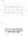
- Figure 1 shows a plane pattern in an embodiment of a field effect transistor relating to the present invention.
- Figure 2 shows vertical cross section of the embodiment.
- Figure 4 is a graph showing a characteristic of drain current of the field effect transistor of the embodiment.
- Figure 3 is a graph showing a characteristic of a drain current of a conventional field effect transistor.
- Figure 1 is a plane pattern of a field effect transistor of this invention, where a plural number of gates G1, G2....and Gn are set between source S and drain D. A conductor for impressing voltage to each gate is led upward, and the electricity is given from the upper positioned layer ( Figure 2). There is no interference of both of source S and drain D positioning in both sides of the gate, and the gate can be given electricity.
- a field effect transistor has an additional function in itself and realizes intensive functions and high density of functions to be equipped in a LSI.
- a field effect transistor relating to this invention establishes a plural number of gates and generates an output by totalizing of characteristics of "gate voltage vs. drain current" of the gates, so it has an effective result realizable a highly intensive function.
Landscapes
- Junction Field-Effect Transistors (AREA)
- Insulated Gate Type Field-Effect Transistor (AREA)
Applications Claiming Priority (2)
| Application Number | Priority Date | Filing Date | Title |
|---|---|---|---|
| JP4179429A JPH0629520A (ja) | 1992-06-12 | 1992-06-12 | 電界効果トランジスタ |
| JP179429/92 | 1992-06-12 |
Publications (3)
| Publication Number | Publication Date |
|---|---|
| EP0577998A2 EP0577998A2 (en) | 1994-01-12 |
| EP0577998A3 EP0577998A3 (enExample) | 1994-02-16 |
| EP0577998B1 true EP0577998B1 (en) | 1998-03-18 |
Family
ID=16065708
Family Applications (1)
| Application Number | Title | Priority Date | Filing Date |
|---|---|---|---|
| EP93109418A Expired - Lifetime EP0577998B1 (en) | 1992-06-12 | 1993-06-11 | Field effect transistor |
Country Status (4)
| Country | Link |
|---|---|
| EP (1) | EP0577998B1 (enExample) |
| JP (1) | JPH0629520A (enExample) |
| KR (1) | KR940001458A (enExample) |
| DE (1) | DE69317480T2 (enExample) |
Family Cites Families (4)
| Publication number | Priority date | Publication date | Assignee | Title |
|---|---|---|---|---|
| US3355598A (en) * | 1964-11-25 | 1967-11-28 | Rca Corp | Integrated logic arrays employing insulated-gate field-effect devices having a common source region and shared gates |
| JPS5753151A (en) * | 1980-09-16 | 1982-03-30 | Nippon Telegr & Teleph Corp <Ntt> | And circuit |
| JPH0695570B2 (ja) * | 1985-02-07 | 1994-11-24 | 三菱電機株式会社 | 半導体集積回路装置 |
| US5005059A (en) * | 1989-05-01 | 1991-04-02 | Motorola, Inc. | Digital-to-analog converting field effect device and circuitry |
-
1992
- 1992-06-12 JP JP4179429A patent/JPH0629520A/ja active Pending
-
1993
- 1993-06-02 KR KR1019930009886A patent/KR940001458A/ko not_active Withdrawn
- 1993-06-11 DE DE69317480T patent/DE69317480T2/de not_active Expired - Fee Related
- 1993-06-11 EP EP93109418A patent/EP0577998B1/en not_active Expired - Lifetime
Also Published As
| Publication number | Publication date |
|---|---|
| EP0577998A3 (enExample) | 1994-02-16 |
| KR940001458A (ko) | 1994-01-11 |
| DE69317480D1 (de) | 1998-04-23 |
| DE69317480T2 (de) | 1998-07-09 |
| JPH0629520A (ja) | 1994-02-04 |
| EP0577998A2 (en) | 1994-01-12 |
Similar Documents
| Publication | Publication Date | Title |
|---|---|---|
| JP2912174B2 (ja) | ライブラリ群及びそれを用いた半導体集積回路 | |
| JP2668981B2 (ja) | 半導体集積回路 | |
| JPS56116670A (en) | Semiconductor integrated circuit device and manufacture thereof | |
| JPS6124250A (ja) | 半導体集積回路装置 | |
| US7257779B2 (en) | Sea-of-cells array of transistors | |
| US5768146A (en) | Method of cell contouring to increase device density | |
| EP0577998B1 (en) | Field effect transistor | |
| US5404035A (en) | Multi-voltage-level master-slice integrated circuit | |
| JPH04216668A (ja) | 半導体集積回路 | |
| JPS61193467A (ja) | 半導体集積回路装置 | |
| TW200633190A (en) | Method for conversion of flash-memory to rom-memory and device with such a converted rom-memory | |
| US20250285696A1 (en) | Silicon brain | |
| US5798541A (en) | Standard semiconductor cell with contoured cell boundary to increase device density | |
| Cook et al. | Comparison of MOSFET logic circuits | |
| JPS59167049A (ja) | 半導体装置 | |
| JPS58166743A (ja) | マスタ−スライス基板 | |
| Goser et al. | Intelligent memories in VLSI | |
| US6683336B1 (en) | Semiconductor integrated circuit, supply method for supplying multiple supply voltages in semiconductor integrated circuit, and record medium for storing program of supply method for supplying multiple supply voltages in semiconductor integrated circuit | |
| JPS5895855A (ja) | 半導体集積回路装置の設計方法 | |
| KR20240112387A (ko) | Pim 구현을 위한 반도체 소자 | |
| KR970018497A (ko) | 반도체 메모리 장치 | |
| TW329052B (en) | Semiconductor device | |
| KR0167684B1 (ko) | 반도체 메모리 소자내의 기준전압 발생회로의 배치 방법 | |
| 장태진 | A Novel Design of Overpass Channel Synapse Array with Ultra-Low Power Operation for Neuromorphic Systems | |
| JPS60247943A (ja) | 半導体集積回路装置 |
Legal Events
| Date | Code | Title | Description |
|---|---|---|---|
| PUAI | Public reference made under article 153(3) epc to a published international application that has entered the european phase |
Free format text: ORIGINAL CODE: 0009012 |
|
| PUAL | Search report despatched |
Free format text: ORIGINAL CODE: 0009013 |
|
| AK | Designated contracting states |
Kind code of ref document: A2 Designated state(s): DE FR GB |
|
| AK | Designated contracting states |
Kind code of ref document: A3 Designated state(s): DE FR GB |
|
| 17P | Request for examination filed |
Effective date: 19940114 |
|
| 17Q | First examination report despatched |
Effective date: 19950104 |
|
| RAP1 | Party data changed (applicant data changed or rights of an application transferred) |
Owner name: SHARP KABUSHIKI KAISHA Owner name: YOZAN INC. |
|
| GRAG | Despatch of communication of intention to grant |
Free format text: ORIGINAL CODE: EPIDOS AGRA |
|
| GRAG | Despatch of communication of intention to grant |
Free format text: ORIGINAL CODE: EPIDOS AGRA |
|
| GRAH | Despatch of communication of intention to grant a patent |
Free format text: ORIGINAL CODE: EPIDOS IGRA |
|
| GRAH | Despatch of communication of intention to grant a patent |
Free format text: ORIGINAL CODE: EPIDOS IGRA |
|
| GRAA | (expected) grant |
Free format text: ORIGINAL CODE: 0009210 |
|
| AK | Designated contracting states |
Kind code of ref document: B1 Designated state(s): DE FR GB |
|
| REF | Corresponds to: |
Ref document number: 69317480 Country of ref document: DE Date of ref document: 19980423 |
|
| PG25 | Lapsed in a contracting state [announced via postgrant information from national office to epo] |
Ref country code: GB Free format text: LAPSE BECAUSE OF NON-PAYMENT OF DUE FEES Effective date: 19980618 |
|
| ET | Fr: translation filed | ||
| PLBE | No opposition filed within time limit |
Free format text: ORIGINAL CODE: 0009261 |
|
| STAA | Information on the status of an ep patent application or granted ep patent |
Free format text: STATUS: NO OPPOSITION FILED WITHIN TIME LIMIT |
|
| GBPC | Gb: european patent ceased through non-payment of renewal fee |
Effective date: 19980618 |
|
| PG25 | Lapsed in a contracting state [announced via postgrant information from national office to epo] |
Ref country code: FR Free format text: LAPSE BECAUSE OF NON-PAYMENT OF DUE FEES Effective date: 19990226 |
|
| 26N | No opposition filed | ||
| PG25 | Lapsed in a contracting state [announced via postgrant information from national office to epo] |
Ref country code: DE Free format text: LAPSE BECAUSE OF NON-PAYMENT OF DUE FEES Effective date: 19990401 |
|
| REG | Reference to a national code |
Ref country code: FR Ref legal event code: ST |