EP0576150A2 - Digitaler Schaltkreis zur Serialisierung sowie Verzügenungsregulator - Google Patents
Digitaler Schaltkreis zur Serialisierung sowie Verzügenungsregulator Download PDFInfo
- Publication number
- EP0576150A2 EP0576150A2 EP93304079A EP93304079A EP0576150A2 EP 0576150 A2 EP0576150 A2 EP 0576150A2 EP 93304079 A EP93304079 A EP 93304079A EP 93304079 A EP93304079 A EP 93304079A EP 0576150 A2 EP0576150 A2 EP 0576150A2
- Authority
- EP
- European Patent Office
- Prior art keywords
- delay
- output
- units
- pulse
- unit
- Prior art date
- Legal status (The legal status is an assumption and is not a legal conclusion. Google has not performed a legal analysis and makes no representation as to the accuracy of the status listed.)
- Withdrawn
Links
Images


Classifications
-
- H—ELECTRICITY
- H04—ELECTRIC COMMUNICATION TECHNIQUE
- H04J—MULTIPLEX COMMUNICATION
- H04J3/00—Time-division multiplex systems
- H04J3/02—Details
- H04J3/04—Distributors combined with modulators or demodulators
- H04J3/047—Distributors with transistors or integrated circuits
-
- H—ELECTRICITY
- H03—ELECTRONIC CIRCUITRY
- H03K—PULSE TECHNIQUE
- H03K5/00—Manipulating of pulses not covered by one of the other main groups of this subclass
- H03K5/13—Arrangements having a single output and transforming input signals into pulses delivered at desired time intervals
- H03K5/135—Arrangements having a single output and transforming input signals into pulses delivered at desired time intervals by the use of time reference signals, e.g. clock signals
-
- H—ELECTRICITY
- H03—ELECTRONIC CIRCUITRY
- H03M—CODING; DECODING; CODE CONVERSION IN GENERAL
- H03M9/00—Parallel/series conversion or vice versa
-
- H—ELECTRICITY
- H04—ELECTRIC COMMUNICATION TECHNIQUE
- H04J—MULTIPLEX COMMUNICATION
- H04J3/00—Time-division multiplex systems
- H04J3/02—Details
- H04J3/06—Synchronising arrangements
- H04J3/0635—Clock or time synchronisation in a network
- H04J3/0685—Clock or time synchronisation in a node; Intranode synchronisation
Definitions
- This invention relates to digital transmission links and particularly to all digital methods and apparatus for data serialization and time delay regulation.
- phase Locked Loops are most frequently employed to produce the bit clock from the local reference clock running at the parallel data frequency (byte rate) for transmitting data at a higher frequency (bit rate).
- PLL Phase Locked Loop
- N-bit parallel data a clock running at N times the parallel data (byte) frequency is required. This N-bit parallel data is often the encoded data since channel encoding is necessary prior to transmission to overcome a variety of transmission impairments for correct data recovery to ensure reliable data transfer.
- phase locked loop used in a transmitting circuit is not as demanding as those used in the receiver circuit for the obvious reason that the input to the PLL is a known frequency from a stable frequency source, however, the problems associated with phase locked loop design such as susceptibility to digital switching noise, and the requirement for analog circuitry and large capacitors and resistors is still present, making it difficult to be integrated with digital functions.
- controlled delay is normally obtained by applying an analog signal as the control signal to a circuit, which is often a filtered or smoothed output from a phase detector.
- a circuit which is often a filtered or smoothed output from a phase detector.
- Traditional methods of constructing phase detector and low pass filters are still valid for these type of delay regulations. These circuits are difficult to provide in integrated circuits and susceptible to noise.
- a digital command control code is used to control or "select" the delay value.
- a finite quantizing error will therefore always exist since the selective delays are discrete values and its accuracy or resolution is determined by the minimum achievable delay values of the basic delay cells.
- Timing delay elements for use as "time rulers" for various timing operations.
- a high speed data serialization circuit for transmitting data onto a serial link which does not require a phase locked loop circuit to generate a multiplexed clock running at serially transmitted bit rate.
- 2N identical delay units for the total delay of N-bit period or a byte period, are cascaded to form the delay line for both the purpose of delay detection and for the purpose of bit stream serialization timing.
- the delay calibration is carried out in such a way that the digital command codes to the delay units are adjusted based on the information from the delay detection logic around the point where it is found that it takes exactly one byte period for a pulse to travel through the entire delay line.
- the delay units are considered to be calibrated to the said nominal value of one half bit period.
- the bit transmitting takes place whenever the pulse arrives at the outputs of every 2 delay units.
- the digital command codes for the controlled delay unit when calibrated, are the codes which can be supplied to other circuits where a time ruler or calibrated delays are required.
- the delay units 21 and 21' which each delay half of the bit period 1/2 Tb, where Tb is the bit period of the serially transmitted data frequency, when calibrated, are cascaded to form the detection delay line 20, outlined by dashed lines.
- a pair of the delay units 21(front unit) and 21'(rear unit) form the bit delay unit which will delay the time of one bit period.
- a single delay unit 22 is used to switch pulse generator 24 to generate a pulse at line 12 for every occurrence of a rising edge of the reference Clock LCLK, the width of which is equal to half of the bit period.
- the output taps from the delay line BT1 through BTN (BT5) are applied to the control terminals of the switches, or the gates of the MOS switches SW1 through SWN (SW5) in the Bit Serializer 30, after the parallel data is latched in the input register 40 and supplied to the bit serializer via line TD1 through TDN (TD5).
- the serialized output data is available from the output of a toggle flip-flop (TFF) 32 on line 38.
- the phase detection delay 50 is where the detection "window center" is located for detailed phase comparison.
- Delay compensation 52 compensates for the delay of the phase detection delay 50 as well as the setup time of the D flip-flops in the sampling register 70.
- Post-delay 60 is used for tracking the pulse when the delay of the delay units are shorter than the nominal value.
- Adjust decision circuit 80 analyzes the sampled status code DST(j:1)71 and makes decisions as when and how to change the controls to the Up/down Shifter 90 which updates the digital command code of the delay units for proper delay adjustment.
- N 5 in connection with FIG. 1 in the following description for the purpose of simplicity in discussion.
- the concepts apply equally to different values of N.
- FDDI Fiber Distributed Data Interface
- 4 bit (half byte) data are first encoded into a 5-bit symbol and then serialized for transmission.
- the local reference clock LCLK 11 runs at the symbol rate which is 1/5 of the bit rate.
- the timing diagram for FIG. 1 the local reference clock LCLK running at the symbol rate is applied to the delay unit 22 and to the pulse generator 24.
- the term "byte” means the coded 5-bit symbol.
- DCK the delayed version of the LCLK, FIG. 2(c), is also supplied to the pulse generator 24 on line 13.
- the pulse generator 24 outputs pulses BT1 for every byte clock period, FIG. 2(g1), and the width of the pulse is determined by the delay value of delay unit 22 which is assumed calibrated to 1/2 Tb.
- the pulse of BT1 travels in the delay line 20 and is delayed for the interval of a bit period each time it arrives at BT2 through BT5, FIG. 2(g2 - g5).
- DBT1 through DBT5 are taps from delay line 20 which provide delayed signals of BT1 through BT5 respectively.
- the functions of DBT1 through DBT5 are explained in connection with the alternate embodiment of FIG. 7.
- the parallel data TDATA(4:0) are latched into the input register and are valid at outputs TD1 through TD5 by the rising edge of DL, FIG.
- TD1 through TD5 are complementaries of TDATA(4:0).
- the first byte is assumed to be an all "one" data byte which is latched for the first byte, FIG. 2(b).
- the latched data TD(5:1) at TD1 through TD5 are then all "0"s.
- Node 33 at the input of invertor 33' is pulled up to high by device 35 if none of the MOS switches SW1-SW5 are on.
- the pulse of BT1 arrives, it turns on MOS switch SW1 for the duration of 1/2 Tb.
- a data bit "0" is transmitted by means of "no transition" in the output signal.
- the design requirement for the TFF 32 is that a matched clock-to-rise (FIG. 2, 331) and clock-to fall (FIG. 2, 332) is desired, or duty cycle distortion type of timing jitter will be added to the transmitted data.
- FIG. 3(a) shows one embodiment of the delay unit 21, which generally consists of two parts: a course step unit 211 and a fine step unit 212.
- the course step unit 211 is formed by two parts: a fixed-stage delay 221 and a variable-stage delay 222.
- FIG. 3(b) which employs 3 invertors.
- the delay from IN to OUT is defined as T step , while the delay from IN to DOUT is defined T dop .
- the delay from the input of the delay cell DV1 (223) to the MUX 225 output DLYM of the variable-stage delay 222 depends on the digital command code on line 232, which selects only one path of MUX 225 from MX1 through MXM to DLYM.
- T int is the "fixed" part of the delay unit, or its intrinsic delay.
- the value of parameter k and m are chosen to guarantee that under all processing and operating conditions, that the unit delay adjustable range is large enough to be able to produce the nominal delay required (1/2Tb).
- T step the delay of the delay cell 250, is the base delay or the minimum adjustable delay of the operation which determines the resolution of the operation.
- T int on the other side is the intrinsic delay of the delay unit which will determine the up-limit of the operating frequency.
- the delay unit 21 could be built by just using the "course" step unit itself if both T step and T int are satisfactory for the frequency targeted.
- the addition of a fine step unit 212 can be beneficial for both higher frequency operation and for lower frequency or larger frequency range operation. For the former, a even finer adjustment than T step is achieved in fine step unit 212 to improve the resolution or to reduce the timing error.
- T step can be chosen a larger value (10x for example).
- delay range amount of 5xT step results for the whole delay line in each coarse step during power-up.
- the delay adjustment also includes the 10 x 1/10 fine steps range of 212 since all fine step units are adjusted simultaneously.
- Another requirement for the delay units is a matched rise-to-rise and fall-to-fall delay to ensure a non-distorted pulse width while a pulse is traveling through the delay line.
- Invertor 213 is used for inverting the polarity of the signal from DLYIN 210 to DLYOUT 220, so for every other delay unit (or a bit time delay) the signal is not inverted and that any mismatches in the rise and fall delays inside the delay unit will be canceled.
- the digital command from the Up/down Shifter on line 1000 controls each of the delay units 21 and 21' such that the delay of which equals to half of the bit period (1/2 Tb), accurate to ⁇ one step in the delay unit, provided that all the delay units are identical and that proper codes are chosen at any particular instance.
- the delay detection is performed by "sampling" the level status by a registration process which looks at each monitored node of delay units from BT3 through delay units 501 through 506 of phase detector 50 and 601 of post delay 60.
- the monitored node is chosen in such a way that the time delay between any two consecutive nodes in any operative condition should be less than 1/2 Tb.
- Sampling Register 70 samples the levels of each monitored node at the rising edge of the LCLK to locate the position of the previous LCLK rising edge.
- the task of locating the position of the previous rising edge could also be accomplished by sequentially setting corresponding RS Flip-Flops which are connected to each of the monitored nodes upon the arrival of the pulse at each monitored node. At the occurrance of the LCLK rising edge, the RS Flip-Flop status can be interrogated to determine the position of the previous rising edge by locating the border between the set and non-set flip-flops.
- the delay of the delay units is very close to the nominal value of 1/2 Tb
- the previous LCLK rising edge should be somewhere around or near the nodes at the interface of delay line 20 and phase detection delay 50, having been delayed the full byte clock period or the delay amount of 2N delay units by the delay line 20.
- a level change indicating a rising edge position is observed in this region when the levels of the monitored nodes are latched into the D type Flip Flop registers clocked by DTRCK.
- This region is where the timing or phase difference between the sampling clock DTRCK on line 14 and the various delayed copies of the sampling clock DN(j:1) needs a close examination, and it is called the detection window.
- the command code to the Delay units is set correctly such that the delay of the delay units are exactly 1/2 Tb
- node WCN, FIG. 4(a) and FIG. 4(b) on the output of delay 503 in the phase detection delay 50 to be the "window center node” where the transition is to occur if the delays are correct when sampling takes place. If the delay of the delay units 21 is not exactly 1/2 Tb, then the transition will be detected on either the left side (indicating "early") or on the right side (indicating "late”) of the window center.
- the same type of delay cells used in delay unit 21 is also used in the phase detection delay 50 (501 through 506).
- the post delay block 60 receives the delayed signal from phase detection delay 50.
- the delays 601, 602, etc. does not have to be the same type of delay units as in block 50 and in fact, delays with larger delay values are preferred since the function of this delay is to "trap" or keep the delayed "previous" LCLK rising transition within the delay line when the current LCLK rising edge is sampling.
- the outputs from the sampling register 70 are the sampled level status for the above nodes and are called DST(j:1)
- DST(j:1) We can show that a "...111...111000" type of this status code can be expected near the node where a "0 -> 1" transition is taking place when it is sampling.
- a "...001110000" type of status code is seen if the signal pulse width is relatively narrow in respect to the delay amount of the delay line.
- WCN is the node around which a level change or transition occurs when the sampling register 70 latches the level status into the DFF's.
- the transition detected will be on one side of the WCN, giving indications whether the delay of the delay unit 21 is shorter or longer than the nominal value.
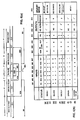
- FIG. 4(b) shows the waveforms at the input of the sampling register 70 and the status is sampled for different timing conditions.
- Line 531 shows the status when the delay units are "calibrated” to their nominal value or the delay line is “in-lock.”
- Line 532 shows the status when the sampling clock DTRCK is "early,” which is equivalent to when the delay of the delay units is larger than their nominal value such that the previous rising transition or the delayed copy 562 has not arrived at WCN.
- Line 533 is for the case the sampling clock is "late” so that the transition 563 has passed WCN.
- the sampled status codes are shown in the matrix of FIG. 4(c). In the "in-lock” condition column, the transition or level status change occurs within -0.5 and +0.5 of WC delay unit range (552).
- the transition occurred between node DD_2 and DD_1 (indicated by a level difference between SD_2 and SD_1, 533) when the sampling clock is sampling. This indicates that the delay of the delay unit is larger than the nominal value and that the control should decrease the delay of the delay unit.
- the delay of the delay units is very close to its nominal value of 1/2 Tb, there is a strong probability that signal at WCN will be making a transition when DTRCK is sampling, 561, FIG. 4(b), causing the flip-flop to enter the metastable state.
- the outputs from the flip-flops DST(J:1) are sampled once every byte, it can allow several bit period times for metastable flip flop resolution, adequate for the output to be settled at one of the two logic states.
- the addition of the phase detection delay 50 to the delay line 20 is to provide a more detailed look at the window center position.
- the additional delay caused by delay units 501 through 503, as well as the setup time of the D flip flops in sampling register 70, is to be compensated by the delay compensation block 52 (FIG.1).
- the calibration of the delay unit includes two modes, the initial "power-up” mode and the normal operation mode.
- the digital command codes may be set initially to maximum such that the delay of the delay unit is maximum or much larger than the nominal 1/2 T b So that fewer delay units are required to delay a byte clock period.
- the "previous" rising edge or the transition of the sampled level status is found on left side of the window center, or somewhere in delay line 20.
- the digital command code 1000 can then be decremented quickly to decrease the delay of the delay units to "move" the detected rising edge transition location quickly towards the WCN.
- This mode is equivalent to the "lock-in" period of the traditional PLL for which smaller loop time constant is desired for fast frequency acquisition.
- FIG. 5 is the block diagram of one embodiment of the Adjust Decision Circuit 80 (FIG. 1.).
- the inputs to this circuit is the status code outputs from the sampling register DST(j:1) which are provided by the sampling process once every byte cycle.
- Complex gate 84 performs the function of rising transition detection. Only if the two inputs to the XOR gate 82 are in different logic levels and the one on the left is a logical one, then the output of the AND gate 83 will be high, indicating a "0 -> 1" transition or a rising edge transition detected between the two consecutive nodes 801 and 802.
- the Status Decode Logic 85 decodes the status code XDST(j:1) into a 7-line detection code on line 851 through 857.
- FIG 6(a) illustrates the function of the Status Decode Logic 85.
- Line 800 indicates the "window center” position. If the detected transition is within the region of -0.5 and +0.5 delay cell from the window center or in the zone D, E, XWC is "1". If the detected transition is in the region of one delay cell on left (right) side of the window center, then XD1 (XU1) is logic "1". If the detected transition is within three delay cells on left (right) of the window center, XD3(XU3) becomes logic "1.” If the transition is in the region one delay cells away on left side of the window center XD(XU) is a logic "1.” Note the overlaps of the regions.
- the status of this detection code combination gives the information as where the transition is detected and how fast this detected transition is moving from byte cycle to cycle. Both are useful when implementing a digital filter function.
- the Adjust Update Control 86, FIG. 5, is not a pure combinatorial logic function, because the output of this circuit is dependent on the current input code combination, and on the history of the input/output.
- the byte clock rate is in the range of ten's of MHz.
- the status sampling rate is much higher than the delay variation rate caused by normal temperature drift or supply voltage variation It is necessary to "filter” out the digital "noise” in the status codes, and to ignore the temporary delay changes caused by high frequency power supply noise.
- Different digital structures can be used to implement the filter function. Generally, the filter function should remove or ignore rapid phase variations caused by rapid electrical noise, while passing the slow and steady phase changes caused by slow delay changes to the controls of the Up/down Shifter 90 to make proper command code adjustment to maintain constant delays of the delay units.
- FIG 6(b) shows a function table for implementing the Adjust Update Control 86, FIG. 5.
- Columns 801 through 807 are the status code inputs from the Status Decode Logic which is sampled for every byte clock.
- Columns 808 through 810 are three intermediate variables.
- Outputs are shown in column 811 through 814 where UD and ROTEN are the control outputs to the Up/down Shifter for delay adjustment.
- FS is the switching control between Fast adjust mode and Slow adjust mode.
- row (a) shows the situation when the detected transition is in zone A, left of XD3, as in the case of power-up.
- This mode corresponds to a smaller time constant as in the PLL case.
- the detected transition is still on the left side of the window center, so decrementing the delay unit is still necessary.
- the transition is already within +- 3 delay units, or +- 3x T step from the window center, in zone B and C in FIG.
- FIG. 6(b) provides a means to understand the overall operation of the adjust update control 86 relative to different zones in which the transition is detected.
- Row (i) and (j) shows error status in which either transitions are detected on both sides of the window center, or none is detected. These error status could be the result of digital noise in the status sampling process, and should therefore be ignored.
- the RESTART becomes active only if the errors are persistently detected. Another error status could result if the adjustable range of the delay unit is large enough that it delays time of Tb instead of 1/2 Tb.
- a IN-LOCK condition could be erroneously resulted since one transition should be detected in the middle of the delay line 20, while a second transition can be detected around the window center.
- This is indicated in row (k) of FIG. 6(b) as a LOCKED-ON-2xUC condition, similar to the case in PLL when the PLL is locked on the second harmonics of the reference clock.
- One solution to this problem is to restart the delay calibration process by setting the control code to the delay units in such a way that all the delay units select minimum delay value as the initial setting. In doing this, the transition is first detected on the right side of the window center to avoid the LOCKED-ON-2xUC condition. Note the "*" in the table in FIG.
- FIG. 7 shows one embodiment of a modified Bit Serializer which allows the selection of the transmitted serial data in either NRZI or NRZ format. If NAZI is selected by enabling NRZI/NRZ, 380, input 381 of mux 31 will be enabled to connect the Q_ output of the D flip-flop 32 to its D input to form a T flip-flop.
- input 383 of mux 31 when input 383 of mux 31 is enabled, it connects XTR to the clock input of flip-flop 32, providing the NRZI output at SERO, 38, as in block 30, FIG. 1. If NRZ is selected, input 382 of mux 31 will be enabled to connect XTR to the D input of flip-flop 32, while input 384 of mux 31' will be enabled to connect NTR to the clock input of flip flop 32. Since node 399 connects switches SW1' through SW5' to ground, a continuous pulse train will be obtained at node NTR, as shown in FIG. 2(k'). In this mode, signal XTR FIG. 2(i'), is the data input to flip-flop 32, and NTR, FIG.
- NTR is generated by the pulse signal when the pulse exists from DBT1 through DBT5 (which are delayed pulses from BT1 through BT5) to turn on switches SW1' through SW5'.
- XTR is generated by the pulse signal when the pulses exist from BT1 through BT5 to turn on SW1 through SW5.
Landscapes
- Engineering & Computer Science (AREA)
- Computer Networks & Wireless Communication (AREA)
- Signal Processing (AREA)
- Theoretical Computer Science (AREA)
- Physics & Mathematics (AREA)
- Nonlinear Science (AREA)
- Microelectronics & Electronic Packaging (AREA)
- Synchronisation In Digital Transmission Systems (AREA)
- Stabilization Of Oscillater, Synchronisation, Frequency Synthesizers (AREA)
- Pulse Circuits (AREA)
Applications Claiming Priority (2)
| Application Number | Priority Date | Filing Date | Title |
|---|---|---|---|
| US901312 | 1992-06-19 | ||
| US07/901,312 US5349612A (en) | 1992-06-19 | 1992-06-19 | Digital serializer and time delay regulator |
Publications (2)
| Publication Number | Publication Date |
|---|---|
| EP0576150A2 true EP0576150A2 (de) | 1993-12-29 |
| EP0576150A3 EP0576150A3 (de) | 1994-04-13 |
Family
ID=25413919
Family Applications (1)
| Application Number | Title | Priority Date | Filing Date |
|---|---|---|---|
| EP93304079A Withdrawn EP0576150A2 (de) | 1992-06-19 | 1993-05-26 | Digitaler Schaltkreis zur Serialisierung sowie Verzügenungsregulator |
Country Status (4)
| Country | Link |
|---|---|
| US (1) | US5349612A (de) |
| EP (1) | EP0576150A2 (de) |
| JP (1) | JPH0661773A (de) |
| TW (1) | TW214585B (de) |
Cited By (9)
| Publication number | Priority date | Publication date | Assignee | Title |
|---|---|---|---|---|
| US5521499A (en) * | 1992-12-23 | 1996-05-28 | Comstream Corporation | Signal controlled phase shifter |
| EP0717496A1 (de) * | 1994-12-13 | 1996-06-19 | Xerox Corporation | Hochgeschwindigkeitsparallel-/Serienschnittstelle |
| FR2735297A1 (fr) * | 1995-06-06 | 1996-12-13 | Mitsubishi Electric Corp | Circuit a retard variable |
| EP0759664A2 (de) * | 1995-08-10 | 1997-02-26 | Mitsubishi Denki Kabushiki Kaisha | Multiplexer und Demultiplexer |
| WO1997016901A1 (en) * | 1995-11-02 | 1997-05-09 | Advanced Intelligence Inc. | Clock signal cleaning circuit |
| EP0686920A3 (de) * | 1994-06-06 | 1997-10-29 | Jeong Deog Kyoon | Serielle Hochgeschwindigkeitsverbindung zur Vollduplex-Datenkommunikation |
| EP0848500A1 (de) * | 1996-12-13 | 1998-06-17 | Siemens Aktiengesellschaft | Parallel/Seriell-Wandler |
| EP0913954A2 (de) * | 1997-11-03 | 1999-05-06 | Advanced Micro Devices, Inc. | Schaltung und Verfahren zur Übertragung von Signalen zwischen Halbleitervorrichtungen |
| WO2000003254A2 (de) * | 1998-07-08 | 2000-01-20 | Infineon Technologies Ag | Schaltung zur ermittlung der zeitdifferenz zwischen flanken eines ersten und eines zweiten digitalen signals |
Families Citing this family (53)
| Publication number | Priority date | Publication date | Assignee | Title |
|---|---|---|---|---|
| US5465065A (en) * | 1993-03-31 | 1995-11-07 | Unisys Corporation | Gate compensation delay and delay lines |
| US5570294A (en) * | 1994-03-11 | 1996-10-29 | Advanced Micro Devices | Circuit configuration employing a compare unit for testing variably controlled delay units |
| US5621705A (en) * | 1994-05-02 | 1997-04-15 | Colorado Seminary | Programmable timing unit for generating multiple coherent timing signals |
| US5769311A (en) * | 1994-08-02 | 1998-06-23 | Toppan Printing Co., Ltd. | Heat insulating cup and method of manufacturing the same |
| US5822386A (en) * | 1995-11-29 | 1998-10-13 | Lucent Technologies Inc. | Phase recovery circuit for high speed and high density applications |
| US5818890A (en) * | 1996-09-24 | 1998-10-06 | Motorola, Inc. | Method for synchronizing signals and structures therefor |
| US5886539A (en) * | 1997-04-10 | 1999-03-23 | Advanced Micro Devices, Ind | Communication within an integrated circuit by data serialization through a metal plane |
| US5963074A (en) * | 1997-06-18 | 1999-10-05 | Credence Systems Corporation | Programmable delay circuit having calibratable delays |
| US5903521A (en) * | 1997-07-11 | 1999-05-11 | Advanced Micro Devices, Inc. | Floating point timer |
| US6122278A (en) * | 1997-08-07 | 2000-09-19 | Advanced Micro Devices, Inc. | Circuit and method for protocol header decoding and packet routing |
| US5943206A (en) * | 1997-08-19 | 1999-08-24 | Advanced Micro Devices, Inc. | Chip temperature protection using delay lines |
| US5890100A (en) * | 1997-08-19 | 1999-03-30 | Advanced Micro Devices, Inc. | Chip temperature monitor using delay lines |
| US6031473A (en) * | 1997-11-17 | 2000-02-29 | Advanced Micro Devices, Inc. | Digital communications using serialized delay line |
| US6084933A (en) * | 1997-11-17 | 2000-07-04 | Advanced Micro Devices, Inc. | Chip operating conditions compensated clock generation |
| US5852616A (en) * | 1997-11-17 | 1998-12-22 | Advanced Micro Devices, Inc. | On-chip operating condition recorder |
| US5942937A (en) * | 1997-11-19 | 1999-08-24 | Advanced Micro Devices, Inc. | Signal detection circuit using a plurality of delay stages with edge detection logic |
| US6046620A (en) * | 1997-12-18 | 2000-04-04 | Advanced Micro Devices, Inc. | Programmable delay line |
| US6178208B1 (en) | 1997-12-18 | 2001-01-23 | Legerity | System for recovery of digital data from amplitude and phase modulated line signals using delay lines |
| US6064232A (en) * | 1997-12-18 | 2000-05-16 | Advanced Micro Devices, Inc. | Self-clocked logic circuit and methodology |
| US6160856A (en) * | 1997-12-18 | 2000-12-12 | Advanced Micro Devices, Inc. | System for providing amplitude and phase modulation of line signals using delay lines |
| US5900834A (en) * | 1997-12-18 | 1999-05-04 | Advanced Micro Devices, Inc. | Doppler shift detector |
| US6255969B1 (en) | 1997-12-18 | 2001-07-03 | Advanced Micro Devices, Inc. | Circuit and method for high speed bit stream capture using a digital delay line |
| US6218880B1 (en) | 1997-12-18 | 2001-04-17 | Legerity | Analog delay line implemented with a digital delay line technique |
| US6078627A (en) * | 1997-12-18 | 2000-06-20 | Advanced Micro Devices, Inc. | Circuit and method for multilevel signal decoding, descrambling, and error detection |
| US6091348A (en) * | 1997-12-18 | 2000-07-18 | Advanced Micro Devices, Inc. | Circuit and method for on-the-fly bit detection and substitution |
| US6088415A (en) * | 1998-02-23 | 2000-07-11 | National Semiconductor Corporation | Apparatus and method to adaptively equalize duty cycle distortion |
| US6339833B1 (en) | 1998-04-17 | 2002-01-15 | Advanced Micro Devices, Inc. | Automatic recovery from clock signal loss |
| US6222392B1 (en) | 1998-04-17 | 2001-04-24 | Advanced Micro Devices, Inc. | Signal monitoring circuit for detecting asynchronous clock loss |
| US6246704B1 (en) * | 1998-04-30 | 2001-06-12 | Stmicroelectronics, Inc. | Automatic on-chip clock tuning methodology and circuitry |
| US6255878B1 (en) | 1998-09-18 | 2001-07-03 | Lsi Logic Corporation | Dual path asynchronous delay circuit |
| US6298315B1 (en) * | 1998-12-11 | 2001-10-02 | Wavecrest Corporation | Method and apparatus for analyzing measurements |
| US6446152B1 (en) * | 1999-03-03 | 2002-09-03 | Nortel Networks Limited | System and method for multi-coupling digital signals and a backplane data bus with multi-coupling of digital signals |
| JP3380206B2 (ja) | 1999-03-31 | 2003-02-24 | 沖電気工業株式会社 | 内部クロック発生回路 |
| JP4310036B2 (ja) * | 2000-09-07 | 2009-08-05 | 株式会社アドバンテスト | タイミング信号発生回路、及び、それを備えた半導体検査装置 |
| US6704882B2 (en) | 2001-01-22 | 2004-03-09 | Mayo Foundation For Medical Education And Research | Data bit-to-clock alignment circuit with first bit capture capability |
| KR100415193B1 (ko) * | 2001-06-01 | 2004-01-16 | 삼성전자주식회사 | 반도체 메모리 장치에서의 내부클럭 발생방법 및 내부클럭발생회로 |
| JP2003050738A (ja) * | 2001-08-03 | 2003-02-21 | Elpida Memory Inc | キャリブレーション方法及びメモリシステム |
| US7088767B1 (en) * | 2002-03-01 | 2006-08-08 | Xilinx, Inc. | Method and apparatus for operating a transceiver in different data rates |
| US20030212837A1 (en) * | 2002-04-25 | 2003-11-13 | Matsushita Elec Ind Co Ltd | Rate converter and rate conversion method |
| US7092471B2 (en) * | 2002-05-22 | 2006-08-15 | Lucent Technologies Inc. | Digital phase synchronization circuit |
| JP4332327B2 (ja) * | 2002-07-05 | 2009-09-16 | テクトロニクス・インターナショナル・セールス・ゲーエムベーハー | データ遅延回路 |
| US6686856B1 (en) * | 2002-11-20 | 2004-02-03 | Agilent Technologies, Inc. | Clocking domain conversion system and method |
| US20040239376A1 (en) * | 2003-05-30 | 2004-12-02 | Haeffele Jeffrey John | Continuously retraining sampler and method of use thereof |
| US7292670B2 (en) * | 2003-08-06 | 2007-11-06 | Gennum Corporation | System and method for automatically correcting duty cycle distortion |
| US7015838B1 (en) * | 2003-09-11 | 2006-03-21 | Xilinx, Inc. | Programmable serializing data path |
| EP1526648A1 (de) * | 2003-10-21 | 2005-04-27 | Mitsubishi Electric Information Technology Centre Europe B.V. | Systeme und Vorrichtung zur Modulation von UWB-Pulssequenzen |
| WO2005048264A1 (en) * | 2003-11-12 | 2005-05-26 | Koninklijke Philips Electronics N.V. | Controlling power consumption peaks in electronic circuits |
| JP2005269147A (ja) * | 2004-03-18 | 2005-09-29 | Sanyo Electric Co Ltd | 遅延回路 |
| US7280930B2 (en) * | 2005-02-07 | 2007-10-09 | Lecroy Corporation | Sequential timebase |
| US7545848B2 (en) * | 2005-11-09 | 2009-06-09 | Agilent Technologies, Inc. | High resolution time stamps for periodic samples |
| CN102064927B (zh) * | 2010-09-21 | 2013-11-13 | 四川和芯微电子股份有限公司 | 时序纠错系统及方法 |
| US9800265B2 (en) * | 2016-03-28 | 2017-10-24 | Novatek Microelectronics Corp. | Data serialization circuit |
| JP7393079B2 (ja) * | 2019-03-26 | 2023-12-06 | ラピスセミコンダクタ株式会社 | 半導体装置 |
Citations (3)
| Publication number | Priority date | Publication date | Assignee | Title |
|---|---|---|---|---|
| WO1989009520A1 (en) * | 1988-03-26 | 1989-10-05 | Alcatel N.V. | Synchronizing circuit |
| DE3843261A1 (de) * | 1988-12-22 | 1990-06-28 | Ant Nachrichtentech | Schaltungsanordnung zur steuerung der phase eines taktsignals |
| EP0384918A1 (de) * | 1989-02-23 | 1990-09-05 | Siemens Aktiengesellschaft | Verfahren und Anordnung zum Anpassen eines Taktes an ein plesiochrones Datensignal und zu dessen Abtakten mit dem angepassten Takt |
Family Cites Families (7)
| Publication number | Priority date | Publication date | Assignee | Title |
|---|---|---|---|---|
| US4524443A (en) * | 1983-12-22 | 1985-06-18 | Sperry Corporation | High speed solid state multiplexer |
| US4805195A (en) * | 1984-06-08 | 1989-02-14 | Amdahl Corporation | Selectable timing delay circuit |
| US4763327A (en) * | 1987-08-17 | 1988-08-09 | Unisys Corporation | Distributed digital signal process multiplexer |
| US4899071A (en) * | 1988-08-02 | 1990-02-06 | Standard Microsystems Corporation | Active delay line circuit |
| US5159205A (en) * | 1990-10-24 | 1992-10-27 | Burr-Brown Corporation | Timing generator circuit including adjustable tapped delay line within phase lock loop to control timing of signals in the tapped delay line |
| US5109394A (en) * | 1990-12-24 | 1992-04-28 | Ncr Corporation | All digital phase locked loop |
| US5146121A (en) * | 1991-10-24 | 1992-09-08 | Northern Telecom Limited | Signal delay apparatus employing a phase locked loop |
-
1992
- 1992-06-19 US US07/901,312 patent/US5349612A/en not_active Expired - Lifetime
- 1992-12-03 TW TW081109691A patent/TW214585B/zh active
-
1993
- 1993-05-26 EP EP93304079A patent/EP0576150A2/de not_active Withdrawn
- 1993-06-17 JP JP5146245A patent/JPH0661773A/ja not_active Withdrawn
Patent Citations (3)
| Publication number | Priority date | Publication date | Assignee | Title |
|---|---|---|---|---|
| WO1989009520A1 (en) * | 1988-03-26 | 1989-10-05 | Alcatel N.V. | Synchronizing circuit |
| DE3843261A1 (de) * | 1988-12-22 | 1990-06-28 | Ant Nachrichtentech | Schaltungsanordnung zur steuerung der phase eines taktsignals |
| EP0384918A1 (de) * | 1989-02-23 | 1990-09-05 | Siemens Aktiengesellschaft | Verfahren und Anordnung zum Anpassen eines Taktes an ein plesiochrones Datensignal und zu dessen Abtakten mit dem angepassten Takt |
Cited By (16)
| Publication number | Priority date | Publication date | Assignee | Title |
|---|---|---|---|---|
| US5521499A (en) * | 1992-12-23 | 1996-05-28 | Comstream Corporation | Signal controlled phase shifter |
| US6211714B1 (en) | 1994-06-06 | 2001-04-03 | Sun Microsystems, Inc. | System for Distributing Clocks |
| EP0686920A3 (de) * | 1994-06-06 | 1997-10-29 | Jeong Deog Kyoon | Serielle Hochgeschwindigkeitsverbindung zur Vollduplex-Datenkommunikation |
| EP0717496A1 (de) * | 1994-12-13 | 1996-06-19 | Xerox Corporation | Hochgeschwindigkeitsparallel-/Serienschnittstelle |
| FR2735297A1 (fr) * | 1995-06-06 | 1996-12-13 | Mitsubishi Electric Corp | Circuit a retard variable |
| EP0759664A2 (de) * | 1995-08-10 | 1997-02-26 | Mitsubishi Denki Kabushiki Kaisha | Multiplexer und Demultiplexer |
| EP0759664A3 (de) * | 1995-08-10 | 1998-01-07 | Mitsubishi Denki Kabushiki Kaisha | Multiplexer und Demultiplexer |
| WO1997016901A1 (en) * | 1995-11-02 | 1997-05-09 | Advanced Intelligence Inc. | Clock signal cleaning circuit |
| US6246276B1 (en) | 1995-11-02 | 2001-06-12 | Advanced Intelligence, Inc. | Clock signal cleaning circuit |
| US5959559A (en) * | 1996-12-13 | 1999-09-28 | Siemens Aktiengesellschaft | Parallel-to-serial converter |
| EP0848500A1 (de) * | 1996-12-13 | 1998-06-17 | Siemens Aktiengesellschaft | Parallel/Seriell-Wandler |
| EP0913954A2 (de) * | 1997-11-03 | 1999-05-06 | Advanced Micro Devices, Inc. | Schaltung und Verfahren zur Übertragung von Signalen zwischen Halbleitervorrichtungen |
| EP0913954A3 (de) * | 1997-11-03 | 2003-09-17 | Advanced Micro Devices, Inc. | Schaltung und Verfahren zur Übertragung von Signalen zwischen Halbleitervorrichtungen |
| WO2000003254A2 (de) * | 1998-07-08 | 2000-01-20 | Infineon Technologies Ag | Schaltung zur ermittlung der zeitdifferenz zwischen flanken eines ersten und eines zweiten digitalen signals |
| WO2000003254A3 (de) * | 1998-07-08 | 2000-02-24 | Siemens Ag | Schaltung zur ermittlung der zeitdifferenz zwischen flanken eines ersten und eines zweiten digitalen signals |
| US7039143B2 (en) | 1998-07-08 | 2006-05-02 | Infineon Technologies Ag | Circuit for determining the time difference between edges of a first digital signal and of a second digital signal |
Also Published As
| Publication number | Publication date |
|---|---|
| US5349612A (en) | 1994-09-20 |
| TW214585B (en) | 1993-10-11 |
| JPH0661773A (ja) | 1994-03-04 |
| EP0576150A3 (de) | 1994-04-13 |
Similar Documents
| Publication | Publication Date | Title |
|---|---|---|
| US5349612A (en) | Digital serializer and time delay regulator | |
| EP0614281B1 (de) | Verfahren und Einrichtung zur digitaler algorithmischer Hochgeschwindigkeitsdatenrückgewinnung | |
| US4584695A (en) | Digital PLL decoder | |
| EP0494984B1 (de) | Phasendetektor für ein system zur taktrückgewinnung mit phasenverriegelungsschleife | |
| US6996202B2 (en) | Multiple channel adaptive data recovery system | |
| US5452333A (en) | Digital jitter correction method and signal preconditioner | |
| US8130891B2 (en) | Clock-data recovery (“CDR”) circuit, apparatus and method for variable frequency data | |
| EP0773653B1 (de) | Verfahren und Einrichtung zur Dekodierung von Manchester-kodierten Daten | |
| EP0185556B1 (de) | Verfahren zur Erzeugung eines digitalen Taktsignals von Manchester-kodierten Signalen | |
| CN1691511B (zh) | 锁相环中的直流偏移的矫正 | |
| US4371974A (en) | NRZ Data phase detector | |
| EP0575059A1 (de) | Wiedergewinnung von digitalen Daten | |
| EP0326007A2 (de) | Digitale phasenverriegelte Schleife mit hoher Auflösung für die zentrale Frequenz | |
| US7170964B2 (en) | Transition insensitive timing recovery method and apparatus | |
| US5349610A (en) | Digital data detecting and synchronizing circuit | |
| CA2096628C (en) | Clock phase alignment | |
| CN100533976C (zh) | 时滞校正装置 | |
| CA1308448C (en) | Method of and circuit arrangement for recovering a bit clock from a received digital communication signal | |
| US6389090B2 (en) | Digital clock/data signal recovery method and apparatus | |
| EP0153107A2 (de) | Gerät und Verfahren zur Taktrückgewinnung für ein ringförmiges Datenübertragungsnetzwerk | |
| US6701140B1 (en) | Digital receive phase lock loop with cumulative phase error correction and dynamically programmable correction rate | |
| US5717728A (en) | Data/clock recovery circuit | |
| US4800340A (en) | Method and apparatus for generating a data recovery window | |
| US7977989B2 (en) | Method and apparatus for detecting and adjusting characteristics of a signal | |
| US4355284A (en) | Phase correction system |
Legal Events
| Date | Code | Title | Description |
|---|---|---|---|
| PUAI | Public reference made under article 153(3) epc to a published international application that has entered the european phase |
Free format text: ORIGINAL CODE: 0009012 |
|
| AK | Designated contracting states |
Kind code of ref document: A2 Designated state(s): BE DE DK ES FR GB GR IE IT LU NL PT |
|
| PUAL | Search report despatched |
Free format text: ORIGINAL CODE: 0009013 |
|
| AK | Designated contracting states |
Kind code of ref document: A3 Designated state(s): BE DE DK ES FR GB GR IE IT LU NL PT |
|
| 17P | Request for examination filed |
Effective date: 19940718 |
|
| 17Q | First examination report despatched |
Effective date: 19970829 |
|
| STAA | Information on the status of an ep patent application or granted ep patent |
Free format text: STATUS: THE APPLICATION IS DEEMED TO BE WITHDRAWN |
|
| 18D | Application deemed to be withdrawn |
Effective date: 20000108 |