EP0572367B1 - Verfahren und Anordnung zur Anpassung der Geschwindigkeit des Auslesens von Daten aus einem Speicher an die Geschwindigkeit des Einschreibens von Daten in den Speicher - Google Patents
Verfahren und Anordnung zur Anpassung der Geschwindigkeit des Auslesens von Daten aus einem Speicher an die Geschwindigkeit des Einschreibens von Daten in den Speicher Download PDFInfo
- Publication number
- EP0572367B1 EP0572367B1 EP19930850104 EP93850104A EP0572367B1 EP 0572367 B1 EP0572367 B1 EP 0572367B1 EP 19930850104 EP19930850104 EP 19930850104 EP 93850104 A EP93850104 A EP 93850104A EP 0572367 B1 EP0572367 B1 EP 0572367B1
- Authority
- EP
- European Patent Office
- Prior art keywords
- addresses
- write
- read
- data information
- memory
- Prior art date
- Legal status (The legal status is an assumption and is not a legal conclusion. Google has not performed a legal analysis and makes no representation as to the accuracy of the status listed.)
- Expired - Lifetime
Links
Images


Classifications
-
- G—PHYSICS
- G06—COMPUTING OR CALCULATING; COUNTING
- G06F—ELECTRIC DIGITAL DATA PROCESSING
- G06F5/00—Methods or arrangements for data conversion without changing the order or content of the data handled
- G06F5/06—Methods or arrangements for data conversion without changing the order or content of the data handled for changing the speed of data flow, i.e. speed regularising or timing, e.g. delay lines, FIFO buffers; over- or underrun control therefor
- G06F5/10—Methods or arrangements for data conversion without changing the order or content of the data handled for changing the speed of data flow, i.e. speed regularising or timing, e.g. delay lines, FIFO buffers; over- or underrun control therefor having a sequence of storage locations each being individually accessible for both enqueue and dequeue operations, e.g. using random access memory
-
- H—ELECTRICITY
- H04—ELECTRIC COMMUNICATION TECHNIQUE
- H04J—MULTIPLEX COMMUNICATION
- H04J3/00—Time-division multiplex systems
- H04J3/02—Details
- H04J3/06—Synchronising arrangements
- H04J3/07—Synchronising arrangements using pulse stuffing for systems with different or fluctuating information rates or bit rates
- H04J3/076—Bit and byte stuffing, e.g. SDH/PDH desynchronisers, bit-leaking
-
- G—PHYSICS
- G06—COMPUTING OR CALCULATING; COUNTING
- G06F—ELECTRIC DIGITAL DATA PROCESSING
- G06F2205/00—Indexing scheme relating to group G06F5/00; Methods or arrangements for data conversion without changing the order or content of the data handled
- G06F2205/06—Indexing scheme relating to groups G06F5/06 - G06F5/16
- G06F2205/061—Adapt frequency, i.e. clock frequency at one side is adapted to clock frequency, or average clock frequency, at the other side; Not pulse stuffing only
Definitions
- the present invention relates to the technical field of memory storage and digital teletransmission. More specifically, the invention relates to a method and an arrangement for adapting the rate at which read addresses are delivered to a memory to the rate at which write addresses are delivered to the same memory, wherein the write addresses are delivered at a rate which is changed intermittently, and wherein the rate at which the read addresses are delivered to the memory is adjusted in a manner such that the read addresses will be delivered to the memory, on average, at the same rate as that at which the write addresses are delivered to the memory.
- the memory may in particular be used for transmitting data information between synchronous and plesiochronous digital hierarchy systems.
- phase locking circuits PLL are used to control the memory read-out rate in a manner such that data will be read from the memory at a rate which is as high as the rate at which data is written into the memory.
- phase locking circuits are used to control the memory read-out rate when the write-in rate varies as a result of deficiencies in the transmission system.
- Phase locking circuits are also used to control the read-out rate of data in those instances when writing of data into the memory is repeatedly interrupted.
- One example of how a phase locking circuit is used is disclosed in U.S. Patent Specification U.S. 4,941,156.
- data information is transmitted from a synchronous digital hierarchy system (SDH) to a plesiochronous digital hierarchy system (PDH) via an addressable memory.
- SDH synchronous digital hierarchy system
- PDH plesiochronous digital hierarchy system
- the data information is divided on frames in the synchronous digital system. These frames include units of data information which are to be transmitted to the PDH-system, and also units of other information which shall not be transmitted.
- the number of data information units can vary with different frames, as a result of adjustments and justifications made in conjunction with the transmission of data between different SDH-systems. These variations are such as to cause the number of data information units to deviate from a nominal number of data information units in a predetermined manner.
- data information is written into an addressable memory, and since the number of data information units may be different in different frames, the information write-in rate is liable to vary.
- Data information written into the addresssable memory is read therefrom into the PDH-system, and when reading data from the memory it is necessary to regulate the read-out rate so that it will be, on average, equally as high as the rate at which information is written into the memory, so that the memory will not become overfilled with data or empty of data.
- a write counter is used to indicate the address at which data shall be written into the memory
- a read counter is used to indicate the address from which data shall be read from the memory. In practice, the read-out rate is therefore controlled by controlling the rate at which read addresses are generated.
- Swedish Patent Application No. 9201672-4 discloses another type of arrangement for regulating the rate at which data is read from an addressable memory, this arrangement having the form of a buffer between an SDH-system and a PDH-system.
- the buffer also includes a write counter which produces write addresses at the rate at which incoming data information enters the memory, and a read counter which produces read addresses from which data shall be read-out from the memory.
- the write-in rate may vary in response to the amount of datainformation contained in the frames, and the object of this arrangement is to control the read-out rate in a manner to follow the varying write-in rate.
- the arrangement includes a mean value counter which is operable to generate mean value addresses around which the write addresses pendulate.
- the generated mean value addresses thus form the mean values of the generated write addresses.
- the arrangement includes a first phase detector for comparison between a generated write address and a simultaneously generated mean value address.
- the generation of mean value addresses is hastened or delayed when the write address deviates excessively from the mean value address as a result of variations in the data write-in rate, so that the write addresses will constantly pendulate around the mean value addresses.
- the mean value counter utilizes a high frequency clock for generating successive mean value addresses.
- the frequency of the high frequency clock is higher than the frequency at which the write addresses are generated, so as to enable the generation of a new mean value address to be hastened or delayed in steps.
- the data read-out rate is regulated by means of a second phase detector, in which each read address gene-rated is compared with the simultaneously generated mean value address, this comparison showing whether or not the data read-out rate is too high. If the read-out rate is too high, the generation of read addresses is stopped temporarily, so that the read-out rate will become as high as the write-in rate.
- a new standard has been formulated in accordance with CCITT in respect of the earlier mentioned transmission systems comprising SDH-systems, PDH-systems and transitions therebetween, for systems which operate at the frequency 155 MHz.
- the new standard concerning the content of the frames has been designated G.703, G.707-709 and G.781-784 respectively.
- the frames in the SDH-system contain respectively data information and other information divided in words each consisting generally of eight bits.
- the amount of datainformation contained in each frame in the SDH-system may correspond to a nominal number of words, or may contain three words more or three words less than the nominal number of words for each frame. Since the amount of datainformation will thus vary from frame to frame, the rate at which information is written into the memory will also vary.
- the amount of data information contained in respective frames may vary between the frames.
- this is because data information is also transmitted between different SDH-systems and it is necessary to equalize any rate differencies between signals in the various SDH-systems when transmitting data.
- Differencies in rates in mutually coacting SDH-systems are equalized in accordance with specifications in the new standard. According to this standard, the rates are equalized by adding to a frame or removing therefrom three words of datainformation in a predetermined manner.
- An object of the present invention is to provide a method of controlling the rate at which information is read from an addressable memory so that this rate, on average, will be equally as high as the rate at which information is written into the memory, without causing troublesome jitter in the event of momentary changes in the write-in rate.
- this object is achieved by the steps of detecting any momentary changes that may occur in the write-in rate, initially masking these detected changes, reducing the masking successively, and regulating or adjusting the read-out rate to the write-in rate, including any masking of changes.
- An arrangement may include detecting means for establishing a change in the rate at which the write addresses are delivered to the memory, a first derivating means for deriving a first comparison magnitude from the write addresses and from a first reference address, a second derivating means for deriving a second comparison magnitude from the read addresses and from a second reference address. These comparison magnitudes are delivered to a control means for regulating the read-out rate in accordance with the relationship between the comparison magnitudes.
- the arrangement also includes activating means for activating the derivation of at least one of the comparison units to a predetermined extent which corresponds to the detected rate change, so as to initially mask the rate change for the control means.
- the activating means functions to reduce the influence of the derivation successively, so that the control means will adjust the read-out rate incrementally, i.e. stepwise, such that said rate will be equally as high as the data write-in rate.
- the inventive embodiments of a method and an arrangement are primarily, but not exclusively, intended for use in conjunction with transitions or transmissions between SDH- and PDH-systems, wherein the addressable memory is included in a buffer between said systems.
- the data information is divided on frames, which include units of data information which is to be transmitted to the PDH-system and also units of other information which is not to be transmitted to the PDH-system.
- the number of data information units contained in each frame may vary from frame to frame, depending on whether the frame contains a nominal number of datainformation units or more data information units or less data information units than said nominal number.
- a write address generator may generate a write address for each unit of data information which is to be transmitted to the PDH-system via the memory. These write addresses are generated in cyclic sequences.
- the read addresses may be generated in cyclic sequences in a read address generator.
- a phase locking circuit is operative to adjust the read-out rate, by adjusting the rate at which read addresses are generated. According to the invention, a change in the rate at which data information enters the memory is detected. When a rate change is detected, i.e.
- phase locking circuit when the number of data information units in an incoming frame is more or less than the nominal number, a corresponding generation of more or less write addresses is initially masked for the phase locking circuit, so that said circuit will not momentarily change the rate at which the read addresses are generated.
- This mask is then removed successively, so as to provide the phase locking circuit incrementally with information to the effect that a change in the write-in rate has been detected and so that the phase locking circuit will adjust the rate at which read addresses are generated in a stepwise manner, i.e. incrementally. Consequently, it is not necessary for the phase locking circuit to quickly carry out very large rate changes, therewith avoiding the risk of troublesome jitter.
- the prime advantage afforded by the invention is that the read-out rate being adjusted in steps, and therewith prevents the problem of jitter occurring.
- the arrangement is also relatively simple to implement and costs can be kept low, since the components used are of a conventional kind.
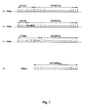
- Figure 1 illustrates how datainformation is distributed on frames in the synchronous system and in the plesiochronous system respectively.
- Figure 2 illustrates a known technique for writing datainformation into a memory and for reading datainformation therefrom.
- Figure 3 illustrates addresses in an addressable memory.
- Figure 4 illustrates an inventive arrangement
- Figures 5a-5c illustrate the cyclic generation of write addresses in three different cases.
- Figure 6 illustrates cyclic generation of read addresses at varying rates.
- Figure 7 illustrates the memory positions with associated addresses in the addressable memory in the inventive arrangement.
- Figure 8 illustrates pulses from a first and a second derivating means included in the inventive arrangement.
- FIGS 9a and 9b illustrate the time shift between pulses delivered by the derivating means.
- Figure 10 is a diagram which illustrates variations in a first reference address.
- a preferred embodiment of a method and an arrangement according to the invention uses and includes respectively a memory, a buffer, between a synchronous digital hierarchy system, a so-called SDH-system, and a plesiochronous digital hierarchy system, a so-called PDH-system.
- the object of the invention is to transmit data information from the SDH-system to the PDH-system via the memory, in a manner such that the rate at which data information is read from the memory will, on average, be equally as high as the rate at which data information is written into the memory.
- the frame Data in in the SDH-system includes units of data information DATAINFO in to be transmitted to the PDH-system, and also units of other information OTHER, which is not to be transmitted to the PDH-system.
- the information in the frames in the SDH-system occur at the frequency of 155 MHz.
- the data information may, for instance, be comprised of speech signals to be transmitted from one telephone subscriber to another.
- the other information which is not to be transmitted to the PDH-system may comprise control information, transmission messages and frame reading words, among other things for controlling the transmission of data information between the SDH-system and the PDH-system.
- the ratio of the number of data information units DATAINFO in and the number of other information units OTHER in each frame may vary, dependending on whether or not the frame contains a nominal number of data information units or more or less data information units than the nominal number.
- the number of data information units DATAINFO in in each frame varies in the case of the illustrated embodiment solely in accordance with the earlier described new standard for signals in SDH-systems.
- One unit in the frame is corresponded by a byte, one word, and a data information byte is transmitted over eight time slots.
- the information is divided into a total of two hundred and seventy bytes per frame, each byte including eight binary coded bits.
- Figure 1a there is shown one frame Data in which contains a nominal number of data information units DATAINFO in and a nominal number of units containing other information OTHER.
- the frame includes two hundred and sixty-one bytes of data information and nine bytes of other information.
- the datainformation appears in the SDH-system at the nominal frequency of 140 MHz.
- other information OTHER may also be incorporated among the data information DATAINFO in , although this has been ignored here in order to simplify the description.
- Figure lb there is shown a frame in which the number of data information units DATAINFO in is greater than the nominal number.
- the frame includes three bytes more data information than is nominal.
- the frame includes three spaces H3 which correspond to twenty-four time slots and which are used to transmit three bytes more data information than is nominal.
- the frame includes in total two hundred and sixty-four bytes of data information.
- the amount of other information OTHER will therewith be smaller than nominal and is corresponded by six bytes instead of nine bytes.
- the data information appears at a frequency which is higher than the nominal frequency.
- Figure 1c there is shown a frame which contains fewer data information units DATAINFO in than is nominal.
- the frame has three bytes less data information than is nominal.
- the frame includes three spaces 0 corresponding to twenty-four time slots which are not used to transmit data information.
- the frame includes in total two hundred and fifty-eight bytes of data information.
- the amount of other information OTHER in the frame of Figure 1c will therewith be greater than is nominal and will correspond to twelve bytes instead of nine bytes. In the case of frames which contain fewer data information units than is nominal in this way, the data information appears at a frequency which is lower than the nominal frequency. Thus, the amount of datainformation contained in the frames illustrated in Figures 1a-1c may vary from frame to frame, meaning that the rate at which data information is written into the addressable memory will also vary correspondingly.
- Figure 1d there is shown a frame Data out which includes data information DATAINFO out which is read wordwise from the memory to the PDH-system.
- the frames Data out which solely contain data information, have different sizes in different applications and in different systems. Outgoing data information is read from the memory at a rate which, on average, corresponds to the data write-in rate.
- FIG. 2 illustrates a known arrangement for writing data information into a memory and for reading data information therefrom.
- the memory 10 which is an addressable memory, is comprised of a FIFO-register (First In First Out) which comprises forty-four memory positions, each of which is intended to store one word.
- the memory 10 has write address inputs 11 for receiving write addresses WADR generated in a write address counter 12, and also includes read address inputs 13 for receiving read addresses RADR generated in a read address counter 14.
- the memory is further provided with data inputs 15 for receiving data information DATAINFO in and data outputs 16 for delivering datainformation DATAINFO out .
- Frames Data in containing data information and other information arrive at an input 17 on a series/parallel converter 18, which delivers the information in words to the data inputs 19 on a Demapper 20.
- An output 21 on the Demapper circuit 20 in connected to an input 22 on the write address counter 12.
- the content of the frames Data in is decoded by the Demapper circuit 20, and a write signal pulse WCLP is delivered to the write address counter 12 for each byte of data information to be written into the memory FIFO, therewith to generate a new write address.
- One word of data information DATAINFO in is written into the memory at the momentary address contained in the write address counter.
- the write addresses WADR, and also the read addresses, are generated cyclicly, as illustrated in Figure 3.
- the addresses are generated in binary coded form at cyclicly repeated intervals.
- the memory has forty-four addresses which range from zero to forty-three and the addresses are binary coded in a manner such that at the transition between address twenty-one and address twenty-two, the most significant bits in the binary code will pass from zero to one, while at the transition between address forty-three and zero, the most significant bit in the binary code will pass from one to zero.
- phase locking circuit uses a phase locking circuit to control the read-out rate from the memory 10.
- This phase locking circuit includes a phase detector 23, a lowpass filter LP and a voltage controlled oscillator VCO.
- the phase detector 23 has a first input 24 on which there is received a first signal which may have either one of two levels, a high level or a low level.
- a second signal which can assume a high or a low level in a corresponding manner is received on a second input 25.
- the phase detector 23 functions to detect the time difference between corresponding level changes, from low to high level, in the first and the second signal and produces on an output a time difference signal td relating to the detected time difference.
- the output of the phase detector 23 is connected to an input on the lowpass filter LP on which the time difference signal td is received.
- the lowpass filter LP there is derived a mean time value from consecutively received time difference signals td.
- An output on the lowpass filter LP is connected to the voltage controlled oscillator VCO.
- the lowpass filter delivers a control signal CO to the voltage controlled oscillator VCO, which produces pulses cl on an output clock at a frequency which depends on the control signal CO.
- the voltage controlled oscillator VCO produces clock pulses cl which may vary in frequency.
- the clock pulses may vary about a nominal frequency which corresponds to the nominal frequency at which data information DATAINFO in appears in the SDH-system.
- the output on the voltage controlled oscillator VCO is connected to an input of a counter 26 which has an output connected to the read address counter 14.
- the clock pulses cl are delivered to the counter 26, which with each eight clock pulses received delivers a read clock puls RCLP to the read address counter 14 for reading-out one word from the address disclosed by the counter content of the read counter 14.
- the first input 24 on the phase detector 23 is connected to the output of an inverting circuit 27, which has an input connected to the most significant bit msb wa on write addresses WADR delivered to the memory 10.
- the second input 25 is connected directly to the most significant bit msb ra on read addresses RADR delivered to the memory 10.
- the aforedescribed known arrangement with which data information is written into and read from a memory in a manner such that the read-out rate is, on average, equally as high as the write-in rate operates in the following manner.
- the write addresses WADR are generated with a shift from the read addresses RADR of one half address cycle, or are shifted from the read addresses as far as possible. This shift is desirable in order for the margins to be as wide as possible, so as to obviate the risk of data being written into and read from one and the same memory position simultaneously when the write-in rate changes.
- the write address zero is generated, the read address 22 is generated simultaneously in a normal operating state, and so on.
- the most significant bit in the binary coded addresses changes its level only twice during an address cycle.
- first address transition which occurs at the transition between addresses twenty-one and twenty-two, when the most significant bit passes from a low to a high level
- second address transition one half address-cycle later, at the transition between the addresses forty-three and zero, when the most significant bit in the binary coded addresses passes from a high to a low level
- the first signal (msb wa ) inv received on the first input 24 of the phase detector derives from the level of the most significant bit on generated write addresses.
- the first signal (msb wa ) inv also corresponds to the inverted level, since it has passed through the inverting circuit 27.
- the second signal msb ra corresponding to the actual level of the most significant bit of generated read addresses is received on the second input 26 of the phase detector.
- the phase detector In the normal state, in which write and read addresses are generated with a phase shift of one half of an address cycle, the first and the second signal switch from a low to a high level simultaneously, since the first signal is inverted.
- the phase detector In a normal state, the phase detector thus receives corresponding level changes from low to high levels in the incoming signals simultaneously, once with each address cycle.
- the corresponding level changes in the most significant bits in generated read and write addresses are thus received simultaneously in the normal state, i.e. when incoming frames solely contain a nominal number of data information units and the write-in rate does not therefore deviate from the nominal write-in rate.
- phase detector 23 delivers to the lowpass filter LP time difference signals td which relate to the time difference between corresponding level changes in the signals arriving at the phase detector 23.
- a mean time value is derived from consecutive time differences td in the lowpass filter. The mean time value thus forms a mean value of deviations from the normal state between generated write addresses and generated read addresses.
- the lowpass filter LP deliver to the voltage controlled oscillator VCO a control signal CO obtained from the derived mean time values, so as to adjust the frequency at which clock pulses cl are delivered from the oscillator VCO and therewith either increase or reduce the rate at which read addresses are generated.
- Data information DATAINFO out is read wordwise from the memory 10 at the rate at which the read addresses are generated.
- the memory data outputs 16 are connected to inputs 28 on a parallel/series-converter P/S which series converts the data information read wordwise from the memory and delivers the information on an output 29 in outgoing frames Data out .
- the phase detector 23 of the known arrangement compares a predetermined first address transition in the sequence of write addresses directly with a predetermined number of second address transitions in the sequence of read addresses. These address transitions differ by one half address cycle, so as to occur simultaneously when the write-in rate is nominal. When a change occurs in the write-in rate and said rate therewith deviates from the nominal rate as earlier described, the address transitions will occur at a given time difference which results in an increase or a decrease in the frequency at which clock pulses c1 are generated, therewith to adjust the read-out rate in keeping with the changed write-in rate. As beforementioned, this momentary change in the read-out rate will result in jitter, for instance. Consequently, an advantage is afforded when using instead an inventive arrangement to transmit data information from an SDH-system to a PDH-system when data information is divided on frames in accordance with the new standard for 155 MHz-signals, or in some similar manner.
- Figure 4 illustrates an embodiment of an inventive arrangement for transmitting data information from a SDH-system to a PDH-system.
- Data information DATAINFO in and other information OTHER occurring in the SDH-system is divided on frames Data in in accordance with the above description made with reference to Figure 1.
- the arrangement illustrated in Figure 4 includes essentially an addressable memory FIFO into which data information is written and from which data information is read, a write address generator WADRGEN, a read address generator RADRGEN, a detecting means DM for establishing a change in the rate at which data information shall be written into the memory, a first derivating means KOMP1, a second derivating means KOMP2, an activating means LC and a phase locking circuit PLL for regulating the rate at which information is read from the memory, so that the read-out rate will, on average, be equally as high as the rate at which information is written into the memory FIFO.
- the addressable memory FIFO delimits the SDH-system from the PDH-system and is used for intermediate storage of data information DATAINFO in when transmitting data between the two systems.
- the memory FIFO includes forty-four eight-bit register or memory positions, each of which has a separate address.
- the memory has eight data inputs 40 for receiving simultaneously the parallel information of eight bits, eight data outputs 41 for delivering the parallel information of eight bits, six write address inputs 42 and six read address inputs 43.
- the write address generator WADRGEN includes a write address counter which counts forwards forty-four six-bit binary write addresses WADR between zero and forty-three at cyclicly repeated intervals. Each write address corresponds to the address of one memory position in the memory FIFO. The memory includes forty-four memory positions, since this number is sufficient for the application concerned.
- the write address generator WADRGEN is provided with six outputs 44 on which the generated write addresses WADR are delivered to the write address inputs 42 on the memory FIFO, wherein data information is written into the FIFO-register at the address disclosed on the write address inputs 42.
- Incoming write clock pulses WCLP are applied to a write pulse input 45, and the write address counter generates a new write address WADR for each write clock pulse, this write address being produced on the outputs 44.
- the read address generator RADRGEN includes a six-bit counter which counts forward forty-four binary read addresses RADR between zero and forty-three at cyclicly repeated intervals, which are the same as those for the write addresses.
- the read address generator RADRGEN is provided with six outputs 46 on which generated read addresses RADR are delivered to the read address inputs 43 on the memory FIFO, wherein data information is read-out from the FIFO-register address disclosed on the read address inputs 43.
- Read clock pulses RCLP are delivered to a read pulse input 47, and the read address counter generates a new read address RADR for each read clock pulse received, this new read address being produced on the output 46.
- the detecting means DM is comprised of a Demapper circuit and has eight data inputs 48 for receiving simultaneously the bits in a word of data information DATAINFO in or other information OTHER, and also has eight data outputs 49 for delivering simultaneously the bits of a word data information DATAINFO in that is to be written into the memory FIFO for further transmission to the PDH-system.
- the data outputs 49 are connected to the data inputs 40 of the memory.
- the detecting means DM is also provided with a first and a second control output 50, 51 for delivering control information concerning the write-in and the read-out of datainformation into and from the memory.
- the second control output 51 is connected to the write pulse input 45 on the write address generator WADRGEN, for delivering write clock pulses WCLP to the write address generator. A write clock pulse is delivered for each word that is to be written into the memory.
- the first deriving means KOMP1 includes a first comparison means, or comparator.
- the deriving means KOMP1 includes nine first inputs 52 to which a first reference address a comprising nine bits is applied. On nine second inputs 53 there is applied a comparison address b which is comprised of the same write address WADR as those supplied to the memory FIFO and three modulo-8-bits.
- the first reference address a is compared in the first comparator with the comparison address b and a comparison magnitude x is delivered on an output 54, this comparison magnitude having the form of a write signal pulse xpls when agreement is found between the first reference address a and the comparison address b .
- the comparison magnitude x is comprised of a signal having a constant level, except when interrupted by a write signal pulse.
- the second deriving means KOMP2 includes a second comparison means or a second comparator.
- a second reference address c which comprises six bits.
- a second comparison address d which is comprised of the same read addresses RADR as those delivered to the memory FIFO, is delivered to six first inputs 55.
- the second reference address c is compared in the second comparator with the second comparison address d and there is delivered on an output 57 a second comparison magnitude y which when similarity is found between the second reference address c and the second comparison address d is comprised of a read signal pulse ypls.
- the second comparison magnitude y is comprised of a signal whose level is constant, except when the signal is broken by a read signal pulse ypls.
- the activating means LC includes a logic circuit having nine outputs 58 which are connected to the input 52 of the first comparator KOMP1, for delivering the first reference address a to the first comparator KOMP1.
- the activating means is also provided with an input 59 which is connected to the first control output 50 for receiving a detection signal DET from the detection signal DM.
- the activating means LC receives from the detection circuit, via the detection signal DET, information which discloses a change in the rate at which data information DATAINFO in is written into the memory FIFO.
- the phase locking circuit PLL includes a phase detector PD, a lowpass filter LP, and a voltage controlled oscillator VCO.
- the phase detector has a first input 70 connected to the output 54 on the first comparator KOMP1 for receiving the first comparison magnitude x .
- the phase detector also has a second input 71, which is connected to the output 57 on the second comparator KOMP2 for receiving the second comparison magnitude y .
- the phase detector PD functions to detect when, in time, the first comparison magnitude x is comprised of a write signal pulse xpls and when, in time, the second comparison magnitude is comprised of a corresponding read signal pulse ypls, and to detect the time difference between corresponding write signal pulses xpls and read signal pulses ypls.
- a time difference signal td which contains information concerning the detected time difference between corresponding write signal pulse xpls and read signal pulse ypls is delivered on output 72 of the phase detector.
- the lowpass filter LP has an input 73 connected to the output 72 of the phase detector, for receiving the time difference signal td.
- a control signal co which contains control information is delivered on an output 74 of the lowpass filter LP to the voltage controlled oscillator VCO. This control information depends on the mean values of the time differences between corresponding write signal pulses and read signal pulses derived in the lowpass filter.
- the voltage controlled oscillator VCO has an input 75 on which the control signal co is received.
- the voltage controlled oscillator VCO produces on an output 76 a clock signal cl which includes clock pulses having a frequency which is dependent on the control information in the control signal co.
- the voltage controlled oscillator VCO delivers clock pulses which may thus vary in frequency.
- the rate of the clock pulses varies around a nominal frequency which corresponds to the nominal rate at which data information DATAINFO in occurs in the SDH-system.
- the inventive arrangement also includes means for writing data information into the memory FIFO and for reading datainformation therefrom.
- the inventive arrangement also includes a series/parallel converter 80 and a modulo-8-counter 81.
- the series/parallel converter 80 has a data input 82 on which earlier described frames Data in containing serial data information DATAINFO in and other information OTHER are received.
- the information contained in the frames Data in arrives at a rate of 155 Mb/s.
- the information contained in the frames Data in is converted in parallel wordwise and is delivered wordwise from the series/parallel converter 80 on eight data outputs 83 connected to corresponding data inputs 48 on the detection circuit DM.
- the modulo-8-counter 81 controls the series/parallel converter in a manner such that the information contained in the frames Data in which enter the series/parallel converter 80 serially, will be delivered on the outputs 83 in words of eight bits.
- the modulo-8-counter 81 has an input 84 on which clock pulses clp having the frequency of 155 MHz are applied.
- the incoming clock pulses clp are also applied to a second input 85 on the series/parallel converter.
- the clock pulses clp have the same frequency as, and are fully synchronous with the information contained in the frames Data in .
- the counter 81 includes three binary bits which are counted forwards from the value zero to the value seven at cyclicly repeating intervals in eight steps.
- the counter steps forward one step for each incoming clock pulse clp.
- the counter 81 has a first output 86 on which the level of the most significant bit msb is delivered to a third input 87 on the series/parallel converter.
- the level of the most significant msb passes from a high to a low level once with each eighth clock pulse clp and this is utilized in the parallel conversion, since each word contains eight bits.
- Eight bits, corresponding to one word, of information are written from the frames Data in into a register in the series/parallel converter. One bit at a time is written into the register over the duration of one clock pulse clp.
- the most significant bit msb passes from a high to a low level at each eighth clock pulse clp and the parallel information in the eight-bit register is then transmitted to the detection circuit DM via the outputs 83.
- the three bits in the modulo-8-counter are delivered on three data outputs 88 connected to three of the second inputs 53 on the first comparitor KOMP1.
- the three bits delivered by the modulo-8-counter constitute the three least significant bits in the first comparison address b .
- the inventive arrangement includes a parallel/series converter 90 and a further modulo-8-counter 91.
- the modulo-8-counter has a clock pulse input 92 connected to the output 76 on the voltage controlled oscillator VCO, for receiving the clock pulses cl from the oscillator.
- the counter 91 has three binary bits and counts from zero to seven with cyclic repetition. The counter is stepped forwards one step with each clock pulse cl and the counter 91 delivers the aforesaid read clock pulse RCLP on an output 93 with each eighth clock pulse.
- the parallel/series converter 90 has eight data inputs 94 connected to the data outputs 41 on the memory FIFO for receiving wordwise datainformation DATAINFO out read-out from the memory FIFO.
- the parallel/series converter 90 has a second input 95 connected to the output on the counter 91, for receiving read clock pulses RCLP.
- a momentary read address is generated for each read clock pulse RCLP and the word data information DATAINFO out which is stored at the momentary address is read-out from the memory to the parallel/series converter 90.
- the information DATAINFO out read-out from the momentary address is stored intermediately in an eight-bit register in the parallel/series converter 90.
- the parallel/series converter 90 has a third input 96 connected to the input 92 of the counter, for receiving the clock pulses cl which control the rate at which information is read-out from the memory FIFO. With each clock pulse cl received, the eight-bit register delivers intermediately stored datainformation DATAOUT out bitwise from the parallel/series converter on a data output 97. The data information DATAOUT out read-out from the register is divided in frames Data out and is transmitted further in the PDH-system on an outgoing line 98. The rate at which the data information occurs in the PDH-system varies around the nominal rate 140 Mb/s.
- the inventive arrangement operates in the following manner.
- Frames Data in containing serial data information DATAINFO in and other information OTHER arrives at the series/parallel converter 80 in the SDH-system.
- the information in the frames Data in is parallel converted in the aforedescribed manner and is delivered wordwise to the detection circuit DM.
- the detection circuit DM decodes the information OTHER in each occurring frame Data in , so as to establish whether or not the frame contains a nominal number of data information units according to Figure 1a or more data information units than this nominal number, according to Figure 1b, or fewer data information units than nominal, according to Figure 1c.
- the other information units OTHER in a frame therefore contain information which discloses whether or not the frame contains a nominal number of data information units DATAINFO in , or fewer data information units than the nominal number or more datainformation units than the nominal number. For instance, two bits in the other information OTHER may disclose the number of data information units in the frame. 00 discloses that the frame contains a nominal number of data information units.
- the detection circuit DM delivers a write clock pulse WCLP to the write address generator WADRGEN for each word of datainformation received.
- the detection circuit DM delivers the write clock pulse signal WCLP when it has received a group of eight-bit datainformation. It is not necessary for these bits to derive from one and the same data information word, but may derive from two words. This is because other information OTHER may be incorporated bitwise in the data information DATAINFO in .
- the write address counter counts forward the next momentary write address WADR in the cyclic sequence with each write clock pulse WCLP received, and when the write address counter delivers the momentary address on the outputs 44, a word comprising eight bits of data information is written into the memory position having the corresponding address.
- this write-in procedure generates successively a cyclic sequence of write addresses WADR in a manner such that a new write address is generated for each data information word to be written into the memory while the generation of write addresses is interrupted with each other information word OTHER.
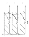
- FIG. 5a-5c illustrate the generation of write addresses in these three separate cases.
- the vertical axis shows the number of write addresses WADR that are generated in one address cycle.
- the horizontal axis shows time t.
- a frame, or more correctly the part of a frame relevant to the present invention includes 258, 261 or 264 data information words which are to be written into the memory. Since an address cycle contains only 44 addresses, several cycles of write addresses WADR are generated for each frame.
- Figures 5a-5c illustrate respectively three different cases of the generation of write addresses WADR and interruption in the generation of write addresses.
- Figure 5a illustrates the generation of write addresses WADR when the occurrent frame Data in contains a nominal number of datainformation words DATAINFO in .
- Several cycles of write addresses WADR are generated prior to time t 0 .
- the first address in the address cycle is generated at time t 0 .
- the generation of write addresses is interrupted between the time points t 1 and t 2 . This interruption extends over that period of time in which a nominal number of other information words OTHER are received in the detection circuit.
- the last write address in the address cycle is generated at time point t 3 .
- Figure 5b illustrates the generation of write addresses WADR when the occurrent frame Data in contains more data information words DATAINFO in than is nominal.
- Several cycles of write addresses WADR are generated prior to time t 0 .
- the first address in the address cycle is generated at time t 0 .
- the generation of write addresses is interrupted for a period of time which is shorter than the interruption made in Figure 5a.
- the interruption extends over that period of time in which a fewer number of other information words OTHER than is nominal are received in the detection circuit DM.
- the last write address in the address cycle is generated at time point t 5 , prior to time point t 3 in Figure 5a.
- Figure 5c illustrates the generation of write addresses WADR when the occurrent frame Data in contains fewer data information words DATAINFO in than is nominal.
- Several cycles of write addresses WADR are generated prior to time t 0 .
- the first address in the address cycle is generated at time t 0 .
- Between the time points t 1 and t 6 there is made a longer pause in the generation of write addresses than the pause made in Figure 5a. This pause extends over the time in which several other information words OTHER than nominal are received in the detection circuit DM.
- the last write address in the address cycle is generated at time point t 7 , after time point t 3 in Figure 5a.
- write addresses WADR are generated in the inventive arrangement in the manner described with reference to Figures 5a-5c.
- the Figures also illustrate how the rate at which the write addresses are generated can vary around the nominal rate illustrated in Figure 5a.
- Data information DATAINFO in is delivered wordwise from the detection circuit DM to the data inputs 40 on the memory FIFO and are written wordwise into the memory FIFO in memory positions disclosed by the write addresses WADR on the write address inputs 42 of the memory FIFO. This write-in of data information takes place in conjunction with the generation of a momentary write address WADR.
- Read addresses RADR are generated continuously, without interruption, when reading data information DATAINFO out from the memory FIFO.
- the rate at which the addresses are generated may vary so as to follow the rate at which write addresses WADR are generated.
- the same memory addresses as the memory addresses in the cyclic sequence of write addresses are included in the sequence of read addresses and in the same order.
- Data information DATAINFOOUT out is read wordwise from memory positions in the memory FIFO disclosed by the read addresses RADR on the read address inputs 43 of the memory FIFO.
- Figure 6 illustrates the continuous generation of read addresses RADR and also shows how the generation rate varies. The illustrated rate variations are greatly exaggerated.
- the vertical axis shows the read addresses RADR of one address cycle.
- the horizontal axis shows time t. All forty-four addresses in an address cycle are generated during the time period A, between the time points t 0 and t 1 , at a nominal rate, which takes place when write addresses are generated at the nominal rate in accordance with the Figure 5a illustration.
- the read addresses RADR in the address cycle are generated at a higher rate than the nominal rate, which takes place when the write addresses WADR are generated at a higher rate than the nominal rate, in the manner shown in the Figure 5b illustration.
- the read addresses RADR in the address cycle are generated at a slower rate than the nominal rate during the time period C, between the time points t 2 and t 3 , which takes place when the write addresses WADR are generated at a lower rate than the nominal rate, as shown in the Figure 5c illustration.
- the memory FIFO is used for writing-in and reading-out data information simultaneously.
- Certain memory positions are used for writing-in information at the same time as other memory positions are used for reading-out information. Consequently, parallel write addresses WADR and read addresses RADR are generated for writing-in and reading-out datainformation.
- WADR and read addresses RADR are generated for writing-in and reading-out datainformation.
- it is highly essential that the momentary addresses in the sequence of write addresses are considerably shifted from the momentary addresses in the sequence of read addresses when generating said addresses. This is to eliminate the possibility of data information being written into and read from the memory at the same memory positions simultaneously.
- the read addresses are generated with a phase shift of one-half address cycle from the simultaneously generated write addresses.
- a momentary mean value AVWADR of consecutive write addresses is generated in the starting state phase shifted through one-half cycle from corresponding momentary read addresses RADR.
- the mean value of generated write addresses is used because the generation of write addresses is not continuous, but includes the aforedescribed interruption. In the starting state, generated write addresses will therefore vary around a write address mean value AVWADR which is shifted through one-half address cycle from corresponding read addresses RADR.
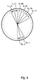
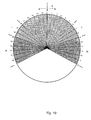
- Figure 7 illustrates an addressable memory FIFO.
- the "cake slices" in the memory shown in Figure 7 illustrate the memory positions with associated addresses.
- An upper arrow illustrates a momentary mean write address value AVWADR, while a bottom arrow illustrates a simultaneous, momentary read address RADR.
- the momentary mean write address value AVWADR and corresponding, simultaneous read addresses RADR are phase shifted through one-half of an address cycle in relation to one another in the Figure 7 illustration.
- the two arrows are continuously displaced clockwise subsequent to the generation of new write addresses and read addresses.
- the momentary mean write address value AVWADR and a momentary, simultaneous mean read address value RADR will be displaced mutually through one-half of an address cycle.
- the rate at which write addresses WADR are generated will also increase. This can be illustrated in Figure 7 by shifting the momentary mean write address value AVWADR clockwise in the drawing, as shown by a third arrow D, thereby reducing the phase difference between the momentary mean value address AVWADR and corresponding read address RADR.
- the inventive arrangement functions to ensure that, on average, the read-out rate will be equally as high as the write-in rate and, therewith, also that the read addresses RADR are generated, on average, at the same rate as the write addresses WADR.
- the first reference address a comprising nine binary bits is formed in the logic circuit in the activating means.
- the reference address a is variable.
- the six most significant bits correspond to a write address.
- the three least significant bits are used to denote eighths of the write addresses.
- the first reference address a is assigned the value zero, corresponding to the write address zero, wherein all nine bits denote the value zero.
- the first reference address a is transmitted from the activating means LC to the first derivation means KOMP1 and stored therein.
- the second reference address c comprising six binary bits which correspond to a write address is stored permanently in the second comparitor or derivation means KOMP2. In the starting state, the second reference c is assigned the value twenty-two.
- the mutual phase shift of the reference addresses a, c in the starting state therewith corresponds to the phase shift between a momentary mean write address value AVWADR and corresponding momentary read addresses RADR in the starting state, i.e. a shift of half an address cycle.
- the first comparitor KOMP1 receives the second comparison address b , which includes the momentary write addresses WADR and three modulo-8-bits from the modulo-8-counter 81.
- the first reference address a is compared continuously in the comparitor KOMP1 with the first comparison address b and the result of the comparison denotes the first comparison magnitude x.
- a write signal pulse xpls is sent from the comparitor KOMP1 to the phase detector PD in the phase-locking circuit PLL.
- a write signal pulse xpls is delivered when the write address WADR and the three modulo-8-bits from the counter 81 are zero. This will therefore occur once with each write address cycle.
- the second comparitor KOMP2 receives the second comparison address d , which includes the momentary read addresses RADR.
- the second reference address c is compared continuously in the comparitor KOMP2 with the second comparison address d , and the comparison result denotes the second comparison magnitude y .
- a read signal pulse ypls is sent from the comparitor KOMP2 to the same phase detector PD. In the starting state, a read signal pulse ypls is transmitted when the read address RADR twenty-two is generated. This therefore occurs once with each read address cycle.
- the write signal pulses xpls are generated, on average, at the same time as the read signal pulses ypls in the starting state of the system, since the phase shift between momentary read addresses RADR and corresponding momentary mean write address values AVWADR correspond to the mutual phase shift of the reference addresses a, c, as illustrated in Figure 8.
- Figure 8 illustrates the write and read signal pulses xpls, ypls delivered by said comparitors KOMP1, KOMP2 when write addresses WADR and read addresses RADR are generated in the starting state of the system.
- the respective vertical axes x and y correspond to the first and the second comparison magnitudes.
- the horizontal axes show time t.
- the comparison magnitudes have a low level, except when the aforesaid pulses are generated.
- the lower diagram shows read signal pulses ypls that are generated at time points t 0 , t 1 , t 2 and t 3 .
- the four read signal pulses are generated during four mutually sequential address cycles, and since the read addresses RADR are generated continuously, the read signal pulses ypls will occur at a constant time interval T between the pulses, in the starting state of the system.
- the read signal pulses ypls are generated when the read address twenty-two is generated in the read address generator RADRGEN.
- the time period between the generation of the read addresses RADR twenty-two in a sequence of address cycles will therefore be constant. Since the write addresses WADR are not generated continuously, but disrupted with pauses, the write signal pulses xpls will, on average, only be generated at the same time as corresponding read signal pulses ypls in the starting state of the system.
- momentary read signal pulses and write signal pulses will not be generated exactly simultaneously with one another, but that a momentary write signal pulse xpls will occur at a given time shift in relation to a corresponding momentary read signal pulse.
- the upper diagram in Figure 8 shows momentary write signal pulses xpls and corresponding momentary read signal pulses ypls. The write signal pulses xpls occur at time points t 00 , t 11 , t 22 and t 33 in four mutually sequential address cycles.
- the momentary read signal pulse ypls occurring at time point t 0 has a corresponding write signal pulse xpls which occurs at time point t 00
- the read signal pulse ypls occurring at time point t 1 has a corresponding write signal pulse xpls at time point t 11 , and so on.
- the write signal pulses xpls occur before the corresponding read signal pulse ypls in two instances and that the write signal pulses occur after corresponding read signal pulses in another two instances.
- the sequence of write pulses xpls shown in the Figure occur, on average, at the same time as the corresponding sequence of read addresses ypls.
- a sequence of momentary write signal pulses xpls is generated, on average, at the same time as the corresponding momentary read signal pulses ypls.
- Figures 9a and 9b show that momentary write signal pulses xpls are, on average, generated with a time shift in relation to corresponding read signal pulses ypls, when the phase shift between momentary read addresses RADR and corresponding mean write address values AVWADR differ from the phase shift between the reference addresses a, c as a result of an increase or a decrease in the rate at which data information is written-in.
- Figure 9a illustrates when the write signal pulses xpls occur in relation to corresponding read signal pulses ypls at a slower write-in rate.
- the write signal pulses xpls will then occur later in comparison with the write signal pulses xpls in the Figure 8 illustration, meaning that the write signal pulses xpls in the Figure 9a illustration are shifted to the right in comparison with the write signal pulses in the Figure 8 illustration.
- the write signal pulses in the Figure 9a illustration occur at the time points t 0+ , t 1- , t 2+ and t 3+ .
- the write signal pulses xpls occur later than the corresponding read signal pulses ypls when the write-in rate decreases.
- Figure 9b illustrates the case when the write signal pulses xpls occur in relation to corresponding read signal pulses ypls at a higher write-in rate.
- the write signal pulses xpls then occur earlier than the write signal pulses xpls in the Figure 8 illustration, which means that the write signal pulses xpls in Figure 9b are shifted to the left in comparison with the write signal pulses in Figure 8.
- the write signal pulses in Figure 9b occur at the time points t 0- , t 1- , t 2 and t 3- .
- the write signal pulses xpls occur earlier than the corresponding read signal pulses ypls when the write-in rate increases.
- the write signal pulses xpls and the read signal pulses ypls are received in the phase detector PD which detects the time difference between a received write signal pulse xpls and corresponding read signal pulse.
- Information concerning detected time differences is sent to the lowpass filter LP, which derives a mean value from detected time differences.
- the time differences diff0, diff1, diff2 and diff3 are detected in Figure 8.
- the average time difference is calculated to zero in the lowpass filter from these values, which means that the rate at which read addresses are generated is equally as high as the rate at which write addresses are generated, which in turn means that the rate at which read addresses RADR are generated shall not be changed.
- control signal co to the voltage controlled oscillator VCO will then contain information to the effect that the rate of the clock pulses cl shall be kept constant. On the other hand, if average time difference exists, positive or negative, the control signal co will contain information to the effect that the rate of the clock pulses cl shall be changed.
- the time differences diff0+, diff2+ and diff3+ are detected instead.
- a mean positive time difference which signifies that write addresses are generated at a slower rate than the rate at which read addresses are generated. This implies that the read address generating rate shall be lowered.
- the control signal co will then contain information to the effect that the clock pulse rate cl shall be lowered, so that read addresses and write addresses are generated at mutually the same rate.
- the time differences diff0-, diff1- and diff3- are detected instead.
- a mean negative time difference which signifies that the write address generating rate is higher than the rate at which read addresses are generated. This implies that the rate at which read addresses are generated shall be increased.
- the control signal co will then contain information to the effect that the clock pulse rate cl shall be increased, so that read addresses and write addresses will be generated at mutually the same rate.
- Masking is effected by changing the first reference address a in a manner which corresponds to the detected change in the number of incoming data information words.
- Information concerning detected changes in the number of data information words in incoming frames Data in is delivered to the activating means, i.e. the logic circuit LC, with two binary bits in the signal DET.
- the signal DET may include three different kinds of information. In a first case, the signal indicates that the first reference address a shall be changed in a positive direction to the same extent as the detected change. This takes place when the incoming frame Data in includes three data information units more than is nominal. For instance, if the reference address a is zero, the address shall be changed to three. In a second case, the first reference address a shall be changed in a negative sense by three addresses.
- the incoming frame Data in includes three data information units fewer than is nominal. For instance, the reference address a is then changed from zero to forty-one. In the third case, the first reference address is left unchanged. This occurs when the incoming frame Data in contains a nominal number of data information units.
- the mutual phase shift between the two reference address a, c is changed to a value which is equally as large as the mean phase shift between generated write addresses and read addresses as a result of the detected rate change.
- the write signal pulses xpls are not shifted from the read signal pulses in the manner illustrated in Figures 9a and 9b, and the write signal pulses xpls will occur, on average, at the same time as the read signal pulses ypls, despite the change in the rate at which write addresses WADR are generated.
- Masking is effected so that the phase-locking circuit PLL will not react immediately to the whole of the rate change that has been detected. As a result of the mask, the phase-locking circuit PLL will not "detect" immediately the change in the write-in rate, since the first reference address a is compensated for the changed write-in rate.
- the read-out rate is adjusted, by finally restoring the first reference address a successively to said starting state.
- the write signal pulses xpls will, on average, be generated with a time shift in relation to corresponding read signal pulses ypls.
- This will result in an adjustment of the readout rate, since the phase detector PD will receive write signal pulses xpls and read signal pulses ypls with a mean time difference, in the manner described with reference to Figures 9a and 9b.
- the phase detector PD receives write signal pulses and read signal pulses with small mean time differences, which results in small successive changes in the read-out rate until said rate is equally as high as the write-in rate.
- first reference address a masking and readjustment
- changes in the first reference address a have been described as being effected by changing the reference address a solely in steps or increments which include complete addresses.
- the reference address a can also be changed in steps which are smaller than complete addresses.
- the first reference address may be divided into eight parts in each address, so that masking and readjustment can be effected in steps in which each step corresponds to one-eighth of the full address.
- the three least significant bits in the first reference address are used to denote one-eighths of complete addresses.
- the six most significant bits denote complete addresses.
- a comparison is made in the first comparitor KOMP1 between the reference address a and the comparison address b , and in order to enable the comparison to be made on a bit level, the comparison address b also includes nine bits.
- the three least significant bits in the comparison address b from the modulo-8-counter 81 enables the comparison to be made on a bit level.
- the three least significant bits in the comparison address are counted eight times for each write address WADR in the comparison address b .
- the reference address a is not changed exactly by three addresses when masking the reference address a , but is changed short of three addresses, or more precisely is changed by two and six-eighths of the addresses.
- the most significant bits are given the binary address two and the least significant bits are given the binary value six.
- each address can be divided into eight parts having mutually different binary values between 000, 001, ..., 111, through the agency of the three least significant bits.
- the reason why the change is short of three addresses instead of being precisely three addresses, is because the SDH-system and the PDH-system have different bit rates.
- the time taken to transmit twenty-four bits of information in the SDH-system is equal to the time taken to transmit twenty-two bits in the PDH-system, since the rate is lower in the PDH-system than in the SDH-system. Thus, when changing the rate in the SDH-system, the corresponding change in the PDH-system is masked.
- the readjustment can also be carried out in eighths of a step with the aid of the three least significant bits in the first reference address a . It is preferred to carry out the readjustment in eighths of a step of complete addresses.
- the reference address a has the binary value two and six-eighths addresses and shall be adjusted back in eighths of a step, the readjustment is thus carried out in twenty-two steps before the reference address a has been returned to the value zero.
- the reference address a is masked in one single step, wherein said first reference address a is changed through a corresponding number of addresses as the detected change in the number of datainformation words in incoming frames Data in .
- the return of the reference address is effected successively, wherein the read-out rate is adjusted. It may happen that a new masking is carried out before the preceding masking has had time to reduce. Consequently, the first reference address a may deviate by more than three addresses from the starting state and must therefore be readjusted at different speeds, depending on the extent in which it deviates from the starting state.
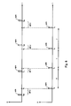
- Figure 10 is a diagram which illustrates those addresses that the first reference address a can assume.
- the reference address a is equal to zero in its starting state.
- the reference address a can be permitted to vary by fifteen addresses in a forwards sense and fifteen addresses in a rearward sense in relation to the address zero.
- the deviation from the starting state should not be greater than said fifteen addresses, because otherwise there is a risk that a given write address WADR will be generated at the same time as the same read address RADR, since the generation of write addresses is displaced in the diagram in the same manner as the reference address a is displaced when changing the write-in rate.
- the reference addresses are divided into five different sectors in the Figure 10 illustration.
- the first sector K includes the addresses 39-6, i.e.
- the second and the third sector L include the addresses 36-38 and 7-9.
- the deviation of the addresses in the L-sectors is further from the starting state than the addresses in the K-sector.
- the fourth and the fifth sectors M include the addresses 30-35 and 10-15.
- the addresses in the M-sectors deviate most from the starting state, when compared with the K-sectors and the L-sectors.
- the readjustment of the reference address a is effected at different speeds, depending on the sector in which the reference address is found.
- the readjustment is effected at a slower rate, meaning, for instance, that the reference address a is changed back towards the starting state at one-eighth of an address at a time, and each adjustment takes place relatively seldomly.
- the reference address has a value within one of the L-sectors
- the address is readjusted at a faster rate, for instance at a rate corresponding to one-eighth of an address at a time, but relatively often.
- readjustment is effected very quickly, so as to avoid the reference address from being located outside the limit addresses 15 and 30.
- the reference address can be readjusted in eighths of a step of addresses and very often. In order to readjust the reference address with sufficient speed, it is possible to readjust in greater steps than eighths of addresses, or even at a speed corresponding to one complete address in one step.
- the readjustment of the first reference address a is effected and controlled by the logic circuit LC.
- both reference addresses a, c are used together to mask a change in the write-in rate, they are together changed by a total number of addresses which equals the change in the number of datainformation units in the incoming frame Data in .
- the readjustment may involve adjusting both reference addresses a, c alternately back to the starting state.
- the invention is not restricted to the aforedescribed and illustrated exemplifying embodiments thereof.
- the invention can be applied in a context in which the number of data information units in a frame can vary in a way different to that described hitherto, for instance such that the data information units DATAINFO in contain two or four more units than the nominal number, or two or four data information units DATAINFO in less than the nominal number.
- the other information OTHER must contain more than two bits in order to indicate this.
- the invention can also be applied in contexts in which the number of data information units DATAINFO in or predetermined changes in the rate at which write addresses are generated/delivered is detected in a manner different to that earlier described.
- it is important that the changes in the rate at which write addresses are delivered to the memory is of a predetermined nature and can be detected/determined in time for the initial compensation.
- purely random changes cannot be masked with an initial compensation according to the present invention.
Landscapes
- Engineering & Computer Science (AREA)
- Theoretical Computer Science (AREA)
- Computer Networks & Wireless Communication (AREA)
- Signal Processing (AREA)
- Physics & Mathematics (AREA)
- General Engineering & Computer Science (AREA)
- General Physics & Mathematics (AREA)
- Synchronisation In Digital Transmission Systems (AREA)
- Time-Division Multiplex Systems (AREA)
Claims (20)
- Verfahren zum Angleichen der Rate mit der eine zyklische Folge von Leseadressen (RADR) an einen Speicher (FIFO) abgegeben wird, und zwar an die Rate, mit der eine zyklische Folge von Schreibadressen (WADR) an den Speicher abgegeben wird, derart, daß die Folge der Schreibadressen mit einer Rate abgegeben wird, die zwischenzeitlich geändert ist, und daß die Rate, mit der die Leseadressen an den Speicher abgegeben wird, so angeglichen wird, daß - im Durchschnitt - die Leseadressen an den Speicher mit derselben Rate wie derjenigen abgegeben werden, mit der Schreibadressen an den Speicher abgegeben werden, gekennzeichnet durch die Schritte:Ableiten einer ersten Vergleichsgröße (x) von der Schreibadresse, derart, daß die erste Vergleichsgröße (x) im Zusammenhang mit der Rate steht, mit der Schreibadressen an den Speicher abgegeben werden,Ableiten einer zweiten Vergleichsgröße (y) aus den Leseadressen, derart, daß die zweite Vergleichsgröße (y) im Zusammenhang mit der Rate steht, mit der Leseadressen an den Speicher abgegeben werden,Ableiten eines Ergebnisses (co) durch Vergleich der ersten und zweiten Vergleichsgröße,Detektieren einer Änderung der Rate, mit der Schreibadressen an den Speicher abgegeben werden,Aktivieren einer erneuten Ableitung mindestens einer der Vergleichsgrößen (x, y) derart, daß das Ergebnis (co) anfänglich unverändert gehalten wird und nachfolgend der Einfluß der erneuten Ableitung reduziert wird, undAngleichen der Rate, mit der Leseadresse an den Speicher in Übereinstimmung mit dem Ergebnis (co) abgegeben werden.
- Verfahren nach Anspruch 1, bei dem die ankommende Dateninformation, die in den Speicher mit Hilfe der Schreibadressen zu schreiben ist, in Rahmen unterteilt wird, derart, daß die Rahmen auch andere Information enthalten, die nicht in den Speicher zu schreiben ist, und derart, daß der Umfang der Dateninformation in dem Rahmen mit einem Nennwert übereinstimmen kann oder von diesem abweichen kann, gekennzeichnet durch das Detektieren der Tatsache, ob der Umfang der Dateninformation, der in einem Rahmen enthalten ist, mit dem Nennwert übereinstimmt oder von dem Nennwert abweicht, um hierdurch die Änderung der Rate zu detektieren, mit der Schreibadressen an den Speicher abzugeben sind.
- Verfahren nach Anspruch 1 oder 2, gekennzeichnet durch die Schritte:Ableiten der ersten Vergleichsgröße (x) aus den Schreibadressen durch Bilden einer ersten Referenzadresse (a), die einer Schreibadresse zugeordnet ist,Vergleichen der Schreibadresse (WADR), die an en Speicher (FIFO) abgegeben wird, mit der ersten Referenzadresse, derart, daß das Vergleichsergebnis die erste Vergleichsgröße (x) bildet,Ableiten der zweiten Vergleichsgröße (y) aus den Leseadressen durch Bilden einer zweiten Referenzadresse (c), die einer Leseadresse zugeordnet ist,Vergleich der Leseadresse (RADR), die an den Speicher (FIFO) abgegeben wird, mit der zweiten Referenzadresse, derart, daß das Vergleichsergebnis die zweite Vergleichsgröße (y) bildet, derart, daß die Referenzadressen (a, c) in einem Startzustand bei Nichtvorliegen der Aktivierung mit einer wechselseitigen Referenz gebildet werden, die allgemein eine Hälfte der zyklischen Phasendifferenz in einer Folge der Adressen übereinstimmt, derart, daß die erste Vergleichsgröße aus einem Schreibsignalpuls (xpls) besteht, der dann erzeugt wird, wenn die Schreibadresse gleich der ersten Referenzadresse ist, und derart, daß die zweite Vergleichsgröße aus einem Lesesignalpuls (ypls) besteht, der erzeugt wird, wenn die Leseadresse gleich der zweiten Referenzadresse ist, wodurch die Pulse (xpls, ypls) gleichzeitig dann erzeugt werden, wenn die Phasenverschiebung zwischen den Leseadressen und den gleichzeitig vorliegenden Schreibadressen mit der Phasenverschiebung zwischen den Referenzadressen übereinstimmt, wodurch die Pulse mit einer Zeitverschiebung dann erzeugt werden, wenn sich die Phasenverschiebungen zwischen abgegebenen Leseadressen und den gleichzeitig erzeugten Schreibadressen gegenüber der Phasenverschiebung zwischen der ersten und zweiten Referenzadresse unterscheiden.
- Verfahren nach Anspruch 3, dadurch gekennzeichnet, daß der Vergleich zwischen der ersten und zweiten Vergleichsgröße (x, y) bewirkt wird, indem ein zeitlicher Vergleich der erzeugten Schreibsignalpulse und Lesesignalpulse (xpls, ypls) durchgeführt wird und die Rate angeglichen wird, mit der neue Leseadressen (RADR) an den Speicher (FIFO) abgegeben werden, in Übereinstimmung mit dem Ergebnis (co) des Vergleichs, derart, daß die Rate dann erhöht wird, wenn der Schreibsignalpuls (xpls), vor dem Lesesignalpulse (ypls) erzeugt wird, und die Rate dann verringert wird, wenn der Schreibsignalpuls nach dem Lesesignalpuls erzeugt wird, und die Rate unverändert dann beibehalten wird, wenn der Schreibsignalpuls und der Lesesignalpuls gleichzeitig zueinander erzeugt werden.
- Verfahren nach Anspruch 3, dadurch gekennzeichnet, daß das Aktivieren der erneuten Ableitung mindestens einer Vergleichsgröße im Zusammenhang mit einer Änderung der Rate, mit der Schreibadressen an den Speicher abgegeben werden, anfänglich bewirkt wird, indem die erste Referenzadresse (a) oder die zweite Referenzadresse (c) oder beide Referenzadressen zusammen (a, c) in einem Umfang verändert werden, der mit der Änderung übereinstimmt; und daß die Aktivierung der erneuten Ableitung sukzessive reduziert wird, indem die geänderte Referenzadresse oder die geänderten Referenzadressen inkrementell stufenweise zu dem Startzustand rückgeführt werden, während der Schreibsignalpuls (xpls) und der Lesesignalpuls (ypls) mit einer Zeitverschiebung erzeugt werden, derart, daß die Rate, mit der Leseadressen an den Speicher abgegeben werden, so angeglichen ist, daß sie der Änderungsrate folgt, mit der Schreibadressen an den Speicher abgegeben werden.
- Anordnung zum Angleichen der Rate, mit der eine zyklische Folge von Leseadressen (RADR) an einen Speicher (FIFO) abgegeben wird, an der Rate, mit der eine zyklische Folge von Schreibadressen (WADR) an den Speicher abgegeben wird, derart, daß die Folge der Schreibadressen mit einer Rate abgegeben wird, die sich zwischenzeitlich ändert, und derart, daß die Anordnung eine Steuervorrichtung (PLL) zum Angleichen der Rate enthält, mit der die Leseadressen an den Speicher abgegeben werden, so daß die Leseadressen im Durchschnitt an den Speicher mit derselben Rate abgegeben werden, wie die Schreibadressen an den Speicher abgegeben werden, gekennzeichnet durcheine erste Ableitvorrichtung (KOMP1) zum Ableiten einer ersten Vergleichsgröße (x) anhand der Schreibadressen, derart, daß die erste Vergleichsgröße (x) im Zusammenhang mit der Rate steht, mit der die Schreibadressen an den Speicher abgegeben werden,eine zweite Ableitvorrichtung (KOMP2), zum Ableiten einer zweiten Vergleichsgröße (y) anhand der Leseadressen, derart, daß die zweite Vergleichsgröße (y) im Zusammenhang mit der Rate steht, mit der die Leseadressen an den Speicher abgegeben werden,eine erste Vergleichsvorrichtung (PD) zum Ableiten eines Ergebnisses (co) durch Vergleich der ersten und zweiten Vergleichsgröße,eine Detektorvorrichtung (DM) zum Detektieren einer Änderung der Rate, mit der Schreibadressen an den Speicher abgegeben werden,eine Aktivierungsvorrichtung (LC) zum Aktivieren eines erneuten Ableitens mindestens einer Vergleichsgröße (x, y) derart, daß das Ergebnis (co) anfänglich unverändert gehalten wird und sukzessive der Einfluß des erneuten Ableitens reduziert ist, undeine Steuervorrichtung (PLL) zum Anglichen der Rate, mit der die Adressen an den Speicher abgegeben werden, in Übereinstimmung mit dem Ergebnis (co).
- Anordnung nach Anspruch 6, bei der Dateninformation, die in den Speicher mit Hilfe der Schreibadressen zu schreiben ist, in Rahmen unterteilt auftritt, derart, daß die Rahmen auch andere Information enthalten, die nicht in den Speicher zu schreiben ist, dadurch gekennzeichnet, daß die Detektionsvorrichtung (DM) zum Detektieren der Änderung der Rate ausgebildet ist, mit der Schreibadressen an Speicher abgegeben werden, durch Detektieren der Tatsache, ob der Umfang der Dateninformation in einem Rahmen mit dem Nennwert übereinstimmt oder nicht oder ob er von dem Wert abweicht.
- Anordnung nach Anspruch 6 oder 7, dadurch gekennzeichnet, daß die erste Ableitvorrichtung (KOMP1) einen ersten Komparator enthält, an dem eine erste Referenzadresse (a) abgegeben wird und an dem auch die gleichen Schreibadressen (WADR) abgegeben werden, wie sie an den Speicher (FIFO) abgegeben werden, derart, daß der Komparator zum Vergleichen der ersten hierin abgegebenen Referenzadresse mit den hierin abgegebenen Schreibadressen gedacht ist, sowie zum Abgeben der ersten Vergleichsgröße (x) in der Form eines Schreibsignalpulse (xpls), wenn eine Übereinstimmung mit der Referenzadresse und den Schreibadressen festgestellt wird; und daß die zweite Ableitvorrichtung (KOMP2) einen zweiten Komparator enthält, an dem eine zweite Referenzadresse (c) abgegeben wird und dieselben Leseadressen (RADR), wie sie an den Speicher (FIFO) abgegeben werden, derart, daß der zweite Komparator funktionsgemäß die zweite hierin abgegebene Referenzadresse mit den hierin angegebenen Leseadressen vergleicht und die zweite Vergleichsgröße (y) in der Form eines Lesesignalpulses (ypls) dann abgibt, wenn eine Übereinstimmung zwischen der zweiten Referenzadresse und den Leseadressen festgestellt wird.
- Anordnung nach Anspruch 8, dadurch gekennzeichnet, daß die erste Vergleichsvorrichtung einen Phasendetektor (PD) enthält, der den Schreibsignalpuls (xpls) an einem ersten Eingang empfängt und der den Lesesignalpuls (ypls) an einem zweiten Eingang empfängt, derart, daß der Phasendetektor funktionsgemäß gemäß der Zeitverschiebung zwischen einem Schreibsignalpuls und einem zugeordneten Lesesignalpulse detektiert und an einen Ausgang ein Steuersignal (co) abgibt, das von einer detektierten Zeitverschiebung abhängt; und daß die Steuervorrichtung (PLL) einen spannungsgesteuerten Oszillator (VCO) enthält, der das Steuersignal (co) an einem Eingang empfängt und an einem Ausgang ein Signal mit einer Frequenz (f) abgibt, die die Rate bestimmt, mit der Leseadressen an den Speicher abgegeben werden; und daß der spannungsgesteuerte Oszillator (VCO) funktionsgemäß die Rate erhöht, mit der neue Leseadressen an den Speicher (FIFO) abgegeben werden, wenn die Schreibsignalpulse vor den zugeordneten Lesesignalpulsen erzeugt werden; und daß der Oszillator zum Reduzieren der Rate dient, wenn die Schreibsignalpulse nach den zugeordneten Lesesignalpulsen erzeugt werden; und daß der Oszillator zum unveränderten Halten der Rate dann dient, wenn zugeordnete Schreibsignalpulse und Lesesignalpulse zu ein und derselben Zeit erzeugt werden.
- Anordnung nach Anspruch 8, dadurch gekennzeichnet, daß die Aktivierungsvorrichtung (LC) eine Logikschaltung enthält, die bei Detektion einer Änderung der Rate, mit der Schreibadressen abgegeben werden, funktionsgemäß die Änderung kompensiert; und daß die Logikschaltung mit dem ersten Komparator (KOMP1) verbunden ist und zum Bewirken einer Änderung der ersten Referenzadresse (a) in Übereinstimmung mit der Änderung der Rate, mit der Schreibadressen abgegeben werden, aufgebaut ist, derart, daß anfänglich eine Kompensierung der gesamten Änderung erfolgt; und daß die Logikschaltung zum Entfernen der Änderung der Referenzadresse (a) in inkrementellen Schritten aufgebaut ist, derart, daß die Kompensierung sukzessive reduziert wird und verschwindet.
- Verfahren zum Übertragen von Dateninformation von einem synchronen digitalen hierarchischen System (SDH) an ein plesiochones, digitales, hierarchisches System (PDH), derart, daß Dateninformation (DATAINFOin) unter Aufteilung auf Rahmen in dem synchronen System auftritt, und die Rahmeneinheiten der Dateninformation (DATAINFOin) enthalten, die an das PDH-System zu übertragen sind und ebenfalls Einheiten anderer Information, die nicht an das PDH-System zu übertragen ist, ferner derart, daß die Beziehung zwischen der Zahl der Dateninformationseinheiten und der Zahl der anderen Informationseinheiten in jedem Rahmen variieren kann, und zwar in Übereinstimmung mit der Tatsache, ob der Rahmen einen Nennwert der Dateninformationseinheiten enthält oder mehr Dateninformationseinheiten als der Nennwert oder weniger Dateninformationseinheiten als der Nennwert und ferner derart, daß das Verfahren die Schritte zum Schreiben der Dateninformation (DATAINFOin) aus dem synchronen System an einen adressierbaren Speicher (FIFO) enthält, sowie zum Auslesen der Dateninformation (DATAINFOout) an das plesiochrone System ausgehend von dem adressierbaren Speicher, und daß in dem Verfahren eine zyklische Folge von Schreibadressen (WADR) sukzessive in einer Weise erzeugt wird, daß eine Schreibadresse für jede Einheit der an das PDH-System zu übertragenden Dateninformation (DATAINFOin) erzeugt wird, wohingehend die Erzeugung der Schreibadressen für jede Einheit der anderen Information unterbrochen wird, wodurch ein Nennwert der Schreibadressen für jeden Rahmen dann erzeugt wird, wenn ein Rahmen mit einem Nennwert der Dateninformationseinheiten in dem synchronen System auftritt, und mehr Schreibadressen als der Nennwert der Adressen für jeden Rahmen dann erzeugt werden, wenn der auftretende Rahmen mehr Dateninformationseinheiten als der Nennwert enthält, und weniger Schreibadressen als der Nennwert der Adressen für jeden Rahmen dann erzeugt werden, wenn der auftretende Rahmen weniger Dateninformationseinheiten als der Nennwert enthält, derart, daß Dateninformation (DATAINFOin) von dem synchronen System in die Speicherpositionen in dem Speicher geschrieben werden, die durch die Schreibadressen bezeichnet sind, daß eine zyklische Folge der Leseadressen (RADR) erzeugt wird, daß dieselben Speicheradressen, wie die in der zyklischen Folge der Schreibadressen enthaltenen Speicheradressen, in der Folge der Leseadressen in derselben Folge wie die Speicheradressen enthalten ist, daß Dateninformation (DATAINFOout) zu dem plesiochronen System ausgehend von den Speicherpositionen in dem Speicher ausgelesen werden, die durch die Leseadressen (RADR) bezeichnet sind, daß in einem Startzustand die Leseadressen allgemein um eine Hälfte eines Adreßzyklus gegenüber den gleichzeitig erzeugten Schreibadressen erzeugt werden, so daß Daten nicht gleichzeitig in/aus ein und derselben Speicherposition geschrieben und gelesen werden, und daß bei den Verfahren die Leseadressen - im Durchschnitt - mit derselben Rate wie die Schreibadressen erzeugt werden, gekennzeichnet durchBilden einer ersten Referenzadresse (a), die einer Schreibadresse zugeordnet ist, und Bilden einer zweiten Referenzadresse (c), die einer Leseadresse zugeordnet ist, derart, daß die wechselseitige Phasenverschiebung der Referenzadressen (a, c) im wesentlichen mit einer Hälfte eines Adreßzyklus in einem Startzustand übereinstimmt;Erzeugen eines Schreibsignalpulses (xpls) dann, wenn die Schreibadresse (WADR) gleich der ersten Referenzadresse (a) ist, und Erzeugen eines Lesesignalpulses (ypls) dann, wenn die Leseadresse (RADR) gleich der zweiten Referenzadresse (c) ist, wodurch die Pulse (xpls, ypls) wechselseitig gleichzeitig dann erzeugt werden, wenn die Phasenverschiebung zwischen den Leseadressen und den Schreibadressen in Übereinstimmung mit der wechselseitigen Phasenverschiebung der Referenzadressen vorliegt, wodurch die Pulse (xpls, ypls) mit einer Zeitverschiebung dann erzeugt werden, wenn die Phasenverschiebung zwischen den Leseadressen und den Schreibadressen sich von der Phasenverschiebung zwischen den Referenzadressen unterscheidet;Abgeben der Pulse (xpls, ypls) an eine Frequenzregelschaltung (PLL), die funktionsgemäß die Rate angleicht, mit der neue Leseadressen (RADR) erzeugt werden, derart, daß die Rate dann verändert wird, wenn der Schreibsignalpuls (xpls) und der zugeordnete Lesesignalpuls (ypls) mit wechselseitiger Zeitverschiebung erzeugt werden, und daß die Rate unverändert dann bleibt, wenn der Schreibsignalpuls (xpls) zur selben Zeit wie der Lesesignalpuls (ypls) erzeugt wird;Detektieren des Zeitpunkts, zu dem ein auftretender Rahmen mehr oder mehr Dateninformationseinheiten (DATAINFOin) als der Nennwert enthält;bei Detektieren der Tatsache, daß ein Rahmen mehr oder weniger Dateninformationseinheiten als der Nennwert aufweist, Maskieren der zugeordneten Erzeugung mehrerer oder weniger Schreibadressen (WADR) für den Rahmen durch Ändern der ersten Referenzadresse (a) oder der zweiten Referenzadresse (a, c) oder beider Referenzadressen zusammen (c) gemäß so vielen Referenzadressen wie der Zahl in Übereinstimmung der mehrerer oder weniger Dateninformationseinheiten;Angleichen der veränderten Referenzadresse oder Referenzadressen (a, c) stufenweise zurück zu dem Startzustand, derart, daß der Schreibsignalpuls (xpls) und der Lesesignalpuls (ypls) mit wechselseitiger Zeitverschiebung so erzeugt werden, daß die Rate, mit der Leseadressen (RADR) erzeugt werden, verändert ist, damit ein Nachführen erfolgt, und zwar zu der Änderung der Zahl der Schreibadressen (WADR), die für jeden Rahmen erzeugt werden, der mit mehr oder weniger Dateninformationseinheiten als die Nenngröße in einem Rahmen auftritt, derart, daß die Rate dann zunimmt, wenn der Rahmen mehr Informationseinheiten enthält, und sie abnimmt, wenn der Rahmen weniger Einheiten als der Nennrahmenwert aufweist.
- Verfahren nach Anspruch 11, dadurch gekennzeichnet, daß bei Detektion mehrerer Dateninformationseinheiten als der Nennwert ebenfalls detektiert wird, daß ein oder mehrere erste Leerstellen (H3) in dem Rahmen vorliegen, mit der Absicht zum Übertragen mehrerer Dateninformationseinheiten als dem Nennwert zugeordnete Dateninformation, und daß bei Detektieren weniger Dateninformationseinheiten als der Nennwert detektiert wird, daß einer oder mehrere Leerstellen (0) in dem Rahmen keine Dateninformation enthalten und nicht für Dateninformation eingesetzt werden, wenn weniger Dateninformationseinheiten als der Nennwert übertragen werden.
- Verfahren nach Anspruch 11, dadurch gekennzeichnet, daß dann, wenn der ankommende Rahmen weniger Dateninformationseinheiten (DATAINFOin) als der Nennwert enthält, die zugeordnete Erzeugung mehrerer Schreibadressen durch Ändern der ersten Referenzadresse (a) in Vorwärtsrichtung maskiert wird, und zwar um so viele Referenzadressen, wie der Zahl der mehreren Dateninformationseinheiten in dem Rahmen oberhalb dem Nennwert, und dann, wenn der ankommende Rahmen weniger Dateninformationseinheiten DATAINFOin) als der Nennwert enthält, die zugeordnete Erzeugung von weniger Schreibadressen durch Ändern der ersten Referenzadresse (a) in Rückwärtsrichtung maskiert wird, und zwar um so viele Referenzadressen wie die geringere Zahl der Dateninformationseinheiten in dem Rahmen in Bezug zu dem Nennwert.
- Verfahren nach Anspruch 13, dadurch gekennzeichnet, daß das Maskieren in einem Schritt bewirkt wird.
- Verfahren nach Anspruch 13, dadurch gekennzeichnet, daß die erste Referenzadresse (a) in Rückwärtsrichtung zu dem Startzustand nach dem Bewirken des Maskierungsbetriebs angeglichen wird, derart, daßdas Abweichen der ersten Referenzadresse (a) gegenüber dem Startzustand gemessen wird; unddie erste Referenzadresse (a) in Rückwärtsrichtung an den Startzustand in inkrementellen Schritten in einer Rate angeglichen wird, die mit zunehmenden Abweichungen der ersten Referenzadresse von dem Startzustand größer wird.
- Verfahren nach Anspruch 15, dadurch gekennzeichnet, daß das stufenweise Angleichen der ersten Referenzadresse (a) in Rückwärtsrichtung zu dem Startzustand in Teilen der Referenzadresse bewirkt wird.
- Anordnung zum Übertragen von Dateninformation von einem synchronen, digitalen, hierarchischen System (SDH) an ein plesiochrones, digitales, hierarchisches System (PDH), derart, daß Dateninformation (DATAINFOin) unter Aufteilung auf Rahmen in dem synchronen System auftritt, daß die Rahmeneinheiten der Dateninformation (DATAINFOin) enthalten, die zu dem PDH-System zu übertragen sind, und ebenfalls Einheiten anderer Information, die nicht zu dem PDH-System zu übertragen sind, daß die Beziehung zwischen der Zahl der Dateninformationseinheiten und der Zahl der anderen Informationseinheiten in jedem Rahmen variiert, in Übereinstimmung mit der Tatsache, ob der Rahmen einen Nennwert der Dateninformationseinheiten enthält, oder mehr Dateninformationseinheiten aus dem Nennwert oder weniger Dateninformationseinheiten aus dem Nennwert, und daß bei der Anordnung Dateninformation (DATAINFOin) von dem synchronen System in den adressierbaren Speicher (FIFO) geschrieben wird und Dateninformation (DATAINFOout) zu dem plesiochronen System ausgehend von dem adressierbaren Speicher ausgelesen wird, und daß die Anordnung einen Schreibadreßgenerator (WADRGEN) zum Erzeugen einer zyklischen Abfolge von Schreibadressen (WADR) enthält, damit eine Schreibadresse für jede Einheit der zu den PDH-System zu übertragenden Dateninformation (DATAINFOin) erzeugt wird, wohingehend die Erzeugung der Schreibadressen für jede Einheit der anderen Information unterbrochen ist, wodurch ein Nennwert der Schreibadressen für jeden Rahmen dann erzeugt wird, wenn ein Rahmen mit einem Nennwert der Dateninformationseinheiten in dem synchronen System auftritt, damit mehr Schreibadressen als der Nennwert der Adressen für jeden Rahmen dann erzeugt werden, wenn der auftretende Rahmen mehr Dateninformationseinheiten als der Nennwert enthält, und weniger Schreibadressen als der Nennwert der Adressen für jeden Rahmen dann erzeugt werden, wenn der auftretende Rahmen weniger Dateninformationseinheiten als der Nennwert enthält, derart, daß Dateninformation (DATAINFOin) von dem synchronen System in die Speicherpositionen in dem Speicher geschrieben werden, die durch die Schreibadresse bezeichnet sind, daß die Anordnung ferner einen Leseadreßgenerator (RADRGEN) zum Erzeugen einer zyklischen Folge der Leseadressen (RADR) enthält, derart, daß dieselben Adressen wie die Schreibadressen, die in der zyklischen Folge der Schreibadressen enthalten sind, in der Folge der Leseadressen enthalten sind, sowie in derselben Folge wie die Speicheradressen, daß Dateninformation (DATAINFOout) zu dem plesiochronen System ausgehend von den Speicherpositionen in dem Speicher ausgelesen wird, die durch die Leseadressen (RADR) bezeichnet sind, in einem Startzustand die Leseadressen allgemein um eine Hälfte eines Adreßzyklus gegenüber den gleichzeitig erzeugten Schreibadressen phasenverschoben erzeugt werden, so daß Daten nicht gleichzeitig in/aus derselben Speicherposition geschrieben/gelesen werden, und in der Anordnung (im Durchschnitt) die Leseadressen mit derselben Rate wie die Schreibadressen erzeugt werden, dadurch gekennzeichnet, daß die Anordnung ebenfalls enthält:eine erste Vergleichsvorrichtung (KOMP1) zum Durchführen eines Vergleichs zwischen einer ersten Referenzadresse (a) und erzeugten Schreibadressen (WADR), derart, daß ein Schreibsignalpuls (xpls) an einem Ausgang dann ausgegeben wird, wenn die Schreibadresse die gleiche wie die erste Referenzadresse ist;eine zweite Vergleichsvorrichtung (KOMP2) zum Durchführen eines Vergleichs zwischen einer zweiten Referenzadresse (c) und erzeugten Leseadressen (RADR) derart, daß ein Lesesignalpuls (ypls) an einem Ausgang dann ausgegeben wird, wenn die Leseadresse die gleiche wie die zweite Referenzadresse ist;eine Frequenzreguliervorrichtung (PLL) mit einem Ausgang, der an dem Leseadreßgenerator (RADRGEN) angeschlossen ist, zum Angleichen der Zählrate, mit der Leseadressen erzeugt werden, der ferner den Schreibsignalpuls (xpls) an einem ersten Eingang und den Lesesignalpuls (ypls) an einem zweiten Eingang empfängt, derart, daß die Zählrate dann angeglichen wird, wenn der Schreibsignalpuls (xpls) und der Lesesignalpuls (ypls) mit wechselseitiger Zeitverschiebung empfangen werden, wohingehend die Zählrate unverändert dann bleibt, wenn der Schreibsignalpuls und der Lesesignalpuls gleichzeitig empfangen werden;eine Logikschaltung (LC) die zum Steuern der ersten Referenzadresse (a) gekoppelt ist, oder zum Steuern der zweiten Referenzadresse (c) gekoppelt ist, oder zum gleichzeitigen Steuern sowohl der ersten Referenzadresse (a) als auch der zweiten Referenzadresse (c) gekoppelt ist, derart, daß die Referenzadressen in einem Startzustand eine wechselseitige Phasenverschiebung aufweisen, die mit einer Hälfte eines Adreßzyklus übereinstimmt, daß der Schreibsignalpuls (xpls) und der Lesesignalpuls (ypls) gleichzeitig dann abgegeben werden, wenn zwischen erzeugten Schreibadressen und gleichzeitig erzeugten Leseadressen vorliegende Phasenverschiebung mit der Phasenverschiebung zwischen der ersten und zweiten Referenzadresse übereinstimmt;eine Detektionsschaltung (DM) zum Detektieren mehr oder weniger Dateninformationseinheiten (DATAINFOin) als der Nennwert der Dateninformationseinheiten bei einem ankommenden Rahmen, derart, daß die Detektionsschaltung (DM) einen Ausgang aufweist, der mit einem Eingang der Logikschaltung (LC) verbunden ist, und zwar zum Abgeben eines Detektionssignals (DET) an die Logikschaltung (LC) dann, wenn mehr oder weniger Dateninformationseinheiten als der Nennwert detektiert werden, daß die zugeordnete Erzeugung von mehr oder weniger Schreibadressen für die Frequenzregulierschaltung maskiert wird, und zwar durch einstufiges Ändern der ersten Referenzadresse (a) oder der zweiten Referenzadresse (b) oder der beiden Referenzadressen (a, c) zusammen, um eine solche Zahl von Referenzadressen, die mit der Zahl der mehr oder weniger Dateninformationseinheiten in dem Rahmen übereinstimmt, wonach die veränderte Referenzadresse oder die veränderten Referenzadressen (a, c) in schrittweisen Inkrementen zurück zu dem Startzustand angeglichen werden, während der Schreibsignalpuls (xpls) und der Lesesignalpuls (ypls) mit wechselseitiger Zeitverschiebung erzeugt werden, derart, daß die Zählrate, mit der Leseadressen (RADR) erzeugt werden, in einer solchen Weise verändert wird, daß sie der Änderung der Erzeugung der Schreibadressen (WADR) folgt, die dann auftritt, wenn der ankommende Rahmen mehr oder weniger Dateninformationseinheiten als der Nennwert enthält, und daß die Frequenzregelschaltung (PLL) die Zählrate als Ergebnis der Detektion von mehr Dateneinheiten als dem Nennwert in einem Rahmen erhöht und die Zählrate als Ergebnis der Detektion von weniger Dateninformationseinheiten in dem ankommenden Rahmen als dem Nennwert verringert.
- Anordnung nach Anspruch 17, dadurch gekennzeichnet, daß die Frequenzregelschaltung (PLL) einen PLL-Kreis enthält, mit einem Phasendetektor (PD) zum Detektieren der wechselseitigen Zeitverschiebung des Schreibsignalpulses (xpls) und des Lesesignalpulses (ypls), derart, daß der Phasendetektor (PD) ein Steuersignal (co) abgibt, das von der detektierten Zeitverschiebung abhängt, und ferner einen spannungsgesteuerte Oszillatorschaltung (VCO) enthält, die das Steuersignal (co) empfängt und die Frequenz eines Taktsignals (c1) in Ansprechen auf das empfangene Steuersignal (co) angleicht, und einen Zähler (91), der das Taktsignal (c1) und die Lesesignalpulse (RCLP) an den Leseadreßgenerator (RADRGEN) abgibt, derart, daß die Lesetaktpulse mit einer Frequenz abgegeben werden, die von der wechselseitigen Zeitverschiebung zwischen dem Schreibsignalpuls und dem Lesesignalpuls abhängen, und derart, daß die Zählrate des Leseadreßgenerators mit der Frequenz der Lesetaktpulse variiert.
- Anordnung nach Anspruch 17, dadurch gekennzeichnet, daß die erste und die zweite Vergleichsvorrichtung (KOMP1, KOMP2) Komparatoren sind.
- Anordnung nach Anspruch 17, dadurch gekennzeichnet, daß die Logikschaltung (LC) funktionsgemäß die erste Referenzadresse (a) in eine Vorwärtsrichtung dann ändert, wenn mehr Dateninformationseinheiten bei einem ankommenden Rahmen als der Nennwert für die Einheiten detektiert wird, derart, daß die Referenzadresse in eine Vorwärtsrichtung gemäß so vielen Referenzadressen wie die zusätzliche Zahl der Dateninformationseinheiten oberhalb dem Nennwert geändert wird, und derart, daß die Logikschaltung funktionsgemäß die erste Referenzadresse (a) in einer Rückwärtsrichtung dann ändert, wenn weniger Dateninformationseinheiten detektiert werden, und derart, daß die Referenzadresse in einer Rückwärtsrichtung um soviele Referenzadressen wie die geringere Zahl der Dateninformationseinheiten geändert wird; und daß die Logikschaltung (LC) funktionsgemäß auch die erste Referenzadresse (a) zurück zu dem Startzustand in inkrementellen Schritten so angleicht, daß die Zahl der Schritte und die Zeitperiode zwischen den Schritten von dem Umfang abhängt, gemäß dem die erste Referenzadresseadresse (a) gegenüber dem Starzustand geändert ist, derart, daß die Angleichung mit großen Schritten oder innerhalb kurzen Zeitintervallen zwischen den Schritten dann durchgeführt wird, wenn die Referenzadresse in einem großen Umfang von einem Startzustand abweicht, und daß die in geringen Schritten und mit langen Zeitintervallen zwischen den Schritten dann durchgeführt wird, wenn die Referenzadresse von dem Starzustand lediglich in einem geringen Umfang abweicht.
Applications Claiming Priority (4)
| Application Number | Priority Date | Filing Date | Title |
|---|---|---|---|
| SE9201672 | 1992-05-27 | ||
| SE9201672A SE470392B (sv) | 1992-05-27 | 1992-05-27 | Förfarande och anordning vid inskrivning och utläsning av data i ett minne, förfarande och anordning för överföring av data från ett synkront digitalt hierarkiskt system till ett plesiokront digitalt hierarkiskt system samt förfarande och anordning för att justera takten på utläsning av data från ett FIFO-register |
| SE9202774A SE470472B (sv) | 1992-09-25 | 1992-09-25 | Förfarande och anordning för att anpassa den takt med vilken datainformation utläses från ett minne till den takt med vilken datainformation inskrivs i minnet |
| SE9202774 | 1992-09-25 |
Publications (2)
| Publication Number | Publication Date |
|---|---|
| EP0572367A1 EP0572367A1 (de) | 1993-12-01 |
| EP0572367B1 true EP0572367B1 (de) | 1999-04-21 |
Family
ID=26661435
Family Applications (2)
| Application Number | Title | Priority Date | Filing Date |
|---|---|---|---|
| EP19930850103 Expired - Lifetime EP0572366B1 (de) | 1992-05-27 | 1993-05-14 | Verfahren und Anordnung zum Einschreiben und Auslesen in einem Speicher |
| EP19930850104 Expired - Lifetime EP0572367B1 (de) | 1992-05-27 | 1993-05-14 | Verfahren und Anordnung zur Anpassung der Geschwindigkeit des Auslesens von Daten aus einem Speicher an die Geschwindigkeit des Einschreibens von Daten in den Speicher |
Family Applications Before (1)
| Application Number | Title | Priority Date | Filing Date |
|---|---|---|---|
| EP19930850103 Expired - Lifetime EP0572366B1 (de) | 1992-05-27 | 1993-05-14 | Verfahren und Anordnung zum Einschreiben und Auslesen in einem Speicher |
Country Status (5)
| Country | Link |
|---|---|
| EP (2) | EP0572366B1 (de) |
| AU (2) | AU666005B2 (de) |
| DE (2) | DE69320257T2 (de) |
| ES (1) | ES2121979T3 (de) |
| MX (2) | MX9303094A (de) |
Families Citing this family (10)
| Publication number | Priority date | Publication date | Assignee | Title |
|---|---|---|---|---|
| GB2297639B (en) * | 1992-10-15 | 1996-10-16 | Fujitsu Ltd | Fifo memory devices |
| GB2291230B (en) * | 1992-10-15 | 1996-10-16 | Fujitsu Ltd | Fifo memory devices |
| DE69429574T2 (de) * | 1993-11-10 | 2002-09-26 | Nortel Networks Ltd., St.Laurent | Regelung des Ablaufs von Zeigeranpassungsereignissen |
| SE505380C2 (sv) * | 1995-11-06 | 1997-08-18 | Ericsson Telefon Ab L M | System vid en transmissionsbuffert |
| JPH09167076A (ja) * | 1995-12-15 | 1997-06-24 | Fuji Photo Film Co Ltd | 出力同期方法及び装置 |
| JPH1132042A (ja) * | 1997-07-11 | 1999-02-02 | Fujitsu Ltd | Sdh通信網/既存通信網監視統合装置及び方法 |
| US20020075981A1 (en) * | 2000-12-20 | 2002-06-20 | Benjamim Tang | PLL/DLL dual loop data synchronization |
| DE10121198A1 (de) * | 2001-04-30 | 2002-11-07 | Infineon Technologies Ag | Verfahren und Vorrichtung zur Anpassung der Datenrate eines Datenstroms |
| CN111198874B (zh) * | 2018-11-16 | 2023-07-04 | 中国电信股份有限公司 | 数据处理方法、装置、系统和计算机可读存储介质 |
| US11907119B2 (en) | 2021-07-14 | 2024-02-20 | Micron Technology, Inc. | Array access with receiver masking |
Family Cites Families (10)
| Publication number | Priority date | Publication date | Assignee | Title |
|---|---|---|---|---|
| US4884286A (en) * | 1985-12-12 | 1989-11-28 | Texas Instruments Inc. | Elastic buffer for local area networks |
| US5146477A (en) * | 1987-03-17 | 1992-09-08 | Antonio Cantoni | Jitter control in digital communication links |
| CA1332627C (en) * | 1987-03-17 | 1994-10-18 | Antonio Cantoni | Jitter control in digital communications links |
| US4941156A (en) * | 1987-05-19 | 1990-07-10 | Crystal Semiconductor | Linear jitter attenuator |
| US4764941A (en) * | 1987-05-22 | 1988-08-16 | American Telephone And Telegraph Company, At&T Bell Laboratories | Digital frame synchronizer |
| US4942593A (en) * | 1989-03-16 | 1990-07-17 | Dallas Semiconductor Corporation | Telecommunications interface with improved jitter reporting |
| US5119406A (en) * | 1990-05-30 | 1992-06-02 | At&T Bell Laboratories | Digital signal synchronization employing single elastic store |
| US5052025A (en) * | 1990-08-24 | 1991-09-24 | At&T Bell Laboratories | Synchronous digital signal to asynchronous digital signal desynchronizer |
| DE4027967A1 (de) * | 1990-09-04 | 1992-03-05 | Philips Patentverwaltung | Stopfentscheidungsschaltung fuer eine anordnung zur bitratenanpassung |
| DE4110933A1 (de) * | 1991-04-04 | 1992-10-08 | Philips Patentverwaltung | Uebertragungssystem fuer die synchrone digitale hierachie |
-
1993
- 1993-05-14 DE DE1993620257 patent/DE69320257T2/de not_active Expired - Fee Related
- 1993-05-14 EP EP19930850103 patent/EP0572366B1/de not_active Expired - Lifetime
- 1993-05-14 ES ES93850103T patent/ES2121979T3/es not_active Expired - Lifetime
- 1993-05-14 EP EP19930850104 patent/EP0572367B1/de not_active Expired - Lifetime
- 1993-05-14 DE DE1993624522 patent/DE69324522T2/de not_active Expired - Fee Related
- 1993-05-26 AU AU38795/93A patent/AU666005B2/en not_active Ceased
- 1993-05-26 AU AU38792/93A patent/AU664087B2/en not_active Ceased
- 1993-05-26 MX MX9303094A patent/MX9303094A/es not_active IP Right Cessation
- 1993-05-27 MX MX9303151A patent/MX9303151A/es not_active IP Right Cessation
Also Published As
| Publication number | Publication date |
|---|---|
| EP0572366B1 (de) | 1998-08-12 |
| AU664087B2 (en) | 1995-11-02 |
| AU3879293A (en) | 1993-12-02 |
| DE69324522D1 (de) | 1999-05-27 |
| EP0572366A1 (de) | 1993-12-01 |
| DE69320257D1 (de) | 1998-09-17 |
| AU666005B2 (en) | 1996-01-25 |
| MX9303094A (es) | 1994-06-30 |
| MX9303151A (es) | 1994-06-30 |
| DE69324522T2 (de) | 1999-09-16 |
| EP0572367A1 (de) | 1993-12-01 |
| AU3879593A (en) | 1993-12-02 |
| ES2121979T3 (es) | 1998-12-16 |
| DE69320257T2 (de) | 1999-01-28 |
Similar Documents
| Publication | Publication Date | Title |
|---|---|---|
| US5359605A (en) | Circuit arrangement for adjusting the bit rates of two signals | |
| US4744082A (en) | Multiplexer apparatus having nBmB coder | |
| CA1205587A (en) | Time-division switching unit | |
| US6157659A (en) | Method of and apparatus for multiplexing and demultiplexing digital signal streams | |
| US4694472A (en) | Clock adjustment method and apparatus for synchronous data communications | |
| US5327430A (en) | Circuit arrangement for bit rate adaptation | |
| KR920000165B1 (ko) | 디지탈 프레임 동기 장치 | |
| US4429386A (en) | Buffer arrangement of a PCM exchange system | |
| US5331671A (en) | Circuit arrangement for bit rate adjustment to two digital signals | |
| EP0572367B1 (de) | Verfahren und Anordnung zur Anpassung der Geschwindigkeit des Auslesens von Daten aus einem Speicher an die Geschwindigkeit des Einschreibens von Daten in den Speicher | |
| US5357514A (en) | Distributed bit-by-bit destuffing circuit for byte-stuffed multiframe data | |
| JPH08204666A (ja) | 制御回路付き伝送システム及び比較器付き制御回路 | |
| US5132970A (en) | Bit rate adaptation circuit arrangement comprising a justification decision circuit | |
| US3887769A (en) | Frame syncrhonization of elastic data bit stores | |
| US3652800A (en) | Digital pulse transmission through an analog tdm switching system | |
| EP0514866B1 (de) | Stopfsynchronisationssystem | |
| US20030076911A1 (en) | Receiver apparatus in stuffing synchronization system | |
| GB2128450A (en) | Time-division switching unit | |
| EP1675291B1 (de) | Digitaltaktfilter | |
| US5548624A (en) | Destuff circuit for asynchronous digital signals | |
| JP2697371B2 (ja) | スタッフ多重通信受信回路 | |
| WO1997005719A1 (en) | Broadcast video desynchroniser | |
| SU453726A1 (ru) | Устройство для асинхронного уплотненияканалов связи с временным разделениемсигналов | |
| SE470472B (sv) | Förfarande och anordning för att anpassa den takt med vilken datainformation utläses från ett minne till den takt med vilken datainformation inskrivs i minnet | |
| US5581493A (en) | Device for filtering positive dejustification jitter of a digital bit stream and application thereof to filtering positive and positive-negative dejustification jitter of a digital bit stream |
Legal Events
| Date | Code | Title | Description |
|---|---|---|---|
| PUAI | Public reference made under article 153(3) epc to a published international application that has entered the european phase |
Free format text: ORIGINAL CODE: 0009012 |
|
| AK | Designated contracting states |
Kind code of ref document: A1 Designated state(s): DE ES GB IT |
|
| 17P | Request for examination filed |
Effective date: 19940419 |
|
| 17Q | First examination report despatched |
Effective date: 19970220 |
|
| GRAG | Despatch of communication of intention to grant |
Free format text: ORIGINAL CODE: EPIDOS AGRA |
|
| GRAG | Despatch of communication of intention to grant |
Free format text: ORIGINAL CODE: EPIDOS AGRA |
|
| GRAH | Despatch of communication of intention to grant a patent |
Free format text: ORIGINAL CODE: EPIDOS IGRA |
|
| GRAH | Despatch of communication of intention to grant a patent |
Free format text: ORIGINAL CODE: EPIDOS IGRA |
|
| GRAA | (expected) grant |
Free format text: ORIGINAL CODE: 0009210 |
|
| AK | Designated contracting states |
Kind code of ref document: B1 Designated state(s): DE ES GB IT |
|
| PG25 | Lapsed in a contracting state [announced via postgrant information from national office to epo] |
Ref country code: ES Free format text: THE PATENT HAS BEEN ANNULLED BY A DECISION OF A NATIONAL AUTHORITY Effective date: 19990421 |
|
| REF | Corresponds to: |
Ref document number: 69324522 Country of ref document: DE Date of ref document: 19990527 |
|
| PGFP | Annual fee paid to national office [announced via postgrant information from national office to epo] |
Ref country code: GB Payment date: 19990622 Year of fee payment: 7 |
|
| PGFP | Annual fee paid to national office [announced via postgrant information from national office to epo] |
Ref country code: DE Payment date: 19990623 Year of fee payment: 7 |
|
| PLBE | No opposition filed within time limit |
Free format text: ORIGINAL CODE: 0009261 |
|
| STAA | Information on the status of an ep patent application or granted ep patent |
Free format text: STATUS: NO OPPOSITION FILED WITHIN TIME LIMIT |
|
| 26N | No opposition filed | ||
| PG25 | Lapsed in a contracting state [announced via postgrant information from national office to epo] |
Ref country code: GB Free format text: LAPSE BECAUSE OF NON-PAYMENT OF DUE FEES Effective date: 20000514 |
|
| GBPC | Gb: european patent ceased through non-payment of renewal fee |
Effective date: 20000514 |
|
| PG25 | Lapsed in a contracting state [announced via postgrant information from national office to epo] |
Ref country code: DE Free format text: LAPSE BECAUSE OF NON-PAYMENT OF DUE FEES Effective date: 20010301 |
|
| PG25 | Lapsed in a contracting state [announced via postgrant information from national office to epo] |
Ref country code: IT Free format text: LAPSE BECAUSE OF NON-PAYMENT OF DUE FEES Effective date: 20050514 |