EP0571924A1 - Verfahren zum Verbinden eines optischen Wellenleiters mit einer optischen Faser - Google Patents
Verfahren zum Verbinden eines optischen Wellenleiters mit einer optischen Faser Download PDFInfo
- Publication number
- EP0571924A1 EP0571924A1 EP93108363A EP93108363A EP0571924A1 EP 0571924 A1 EP0571924 A1 EP 0571924A1 EP 93108363 A EP93108363 A EP 93108363A EP 93108363 A EP93108363 A EP 93108363A EP 0571924 A1 EP0571924 A1 EP 0571924A1
- Authority
- EP
- European Patent Office
- Prior art keywords
- fiber
- waveguide
- optical
- marker
- chip
- Prior art date
- Legal status (The legal status is an assumption and is not a legal conclusion. Google has not performed a legal analysis and makes no representation as to the accuracy of the status listed.)
- Granted
Links
Images


Classifications
-
- G—PHYSICS
- G02—OPTICS
- G02B—OPTICAL ELEMENTS, SYSTEMS OR APPARATUS
- G02B6/00—Light guides; Structural details of arrangements comprising light guides and other optical elements, e.g. couplings
- G02B6/24—Coupling light guides
- G02B6/26—Optical coupling means
- G02B6/30—Optical coupling means for use between fibre and thin-film device
-
- G—PHYSICS
- G02—OPTICS
- G02B—OPTICAL ELEMENTS, SYSTEMS OR APPARATUS
- G02B6/00—Light guides; Structural details of arrangements comprising light guides and other optical elements, e.g. couplings
- G02B6/24—Coupling light guides
- G02B6/42—Coupling light guides with opto-electronic elements
- G02B6/4201—Packages, e.g. shape, construction, internal or external details
- G02B6/4219—Mechanical fixtures for holding or positioning the elements relative to each other in the couplings; Alignment methods for the elements, e.g. measuring or observing methods especially used therefor
- G02B6/4228—Passive alignment, i.e. without a detection of the degree of coupling or the position of the elements
- G02B6/423—Passive alignment, i.e. without a detection of the degree of coupling or the position of the elements using guiding surfaces for the alignment
- G02B6/4231—Passive alignment, i.e. without a detection of the degree of coupling or the position of the elements using guiding surfaces for the alignment with intermediate elements, e.g. rods and balls, between the elements
-
- G—PHYSICS
- G02—OPTICS
- G02B—OPTICAL ELEMENTS, SYSTEMS OR APPARATUS
- G02B6/00—Light guides; Structural details of arrangements comprising light guides and other optical elements, e.g. couplings
- G02B6/24—Coupling light guides
- G02B6/42—Coupling light guides with opto-electronic elements
- G02B6/4201—Packages, e.g. shape, construction, internal or external details
- G02B6/4219—Mechanical fixtures for holding or positioning the elements relative to each other in the couplings; Alignment methods for the elements, e.g. measuring or observing methods especially used therefor
- G02B6/422—Active alignment, i.e. moving the elements in response to the detected degree of coupling or position of the elements
- G02B6/4221—Active alignment, i.e. moving the elements in response to the detected degree of coupling or position of the elements involving a visual detection of the position of the elements, e.g. by using a microscope or a camera
- G02B6/4224—Active alignment, i.e. moving the elements in response to the detected degree of coupling or position of the elements involving a visual detection of the position of the elements, e.g. by using a microscope or a camera using visual alignment markings, e.g. index methods
-
- Y—GENERAL TAGGING OF NEW TECHNOLOGICAL DEVELOPMENTS; GENERAL TAGGING OF CROSS-SECTIONAL TECHNOLOGIES SPANNING OVER SEVERAL SECTIONS OF THE IPC; TECHNICAL SUBJECTS COVERED BY FORMER USPC CROSS-REFERENCE ART COLLECTIONS [XRACs] AND DIGESTS
- Y10—TECHNICAL SUBJECTS COVERED BY FORMER USPC
- Y10S—TECHNICAL SUBJECTS COVERED BY FORMER USPC CROSS-REFERENCE ART COLLECTIONS [XRACs] AND DIGESTS
- Y10S359/00—Optical: systems and elements
- Y10S359/90—Methods
Definitions
- the present invention relates to a method of connecting an optical fiber to a planar optical waveguide, and more particularly, to a connection method which permits easy, low-loss connection of an optical fiber to one of planar optical waveguides formed in an optical component.
- optical waveguide chips are used as optical components.
- Optical waveguide chips are generally classified into those in which silica glass is deposited on, e.g., a Si substrate whose refractive index is different from that of the silica glass, to form planar optical waveguides, and those in which semiconductor thin films of various compositions are successively formed on a special semiconductor substrate of, e.g., InGaAsP, to form planar optical waveguides.
- optical fibers are connected to the planar optical waveguides formed in the optical waveguide chip, with each axis thereof aligned with each axis of the planar optical waveguides, so that light can be transmitted from one optical fiber to the other through the planar optical waveguide.
- optical fibers are connected to planar optical waveguides in the following manner: First, the optical waveguide chip is positioned and fixed in a specific casing, and an optical fiber is abutted against one end of the planar optical waveguide. With light entered from the other end of the planar optical waveguide, the optical fiber is shifted relative to the planar optical waveguide, and while the optical fiber is located at a position where the intensity of light transmitted therethrough is a maximum, the fiber is firmly bonded to the planar optical waveguide by an adhesive or the like.
- another optical fiber is connected to the other end of the planar optical waveguide in a similar manner. Namely, with light transmitted through the previously connected optical fiber, the optical fiber to be connected is positioned and bonded to the planar optical waveguide.
- connection method there is employed no particular mechanical member which keeps each axis of optical fiber aligned with each axis of the planar optical waveguides formed in an optical waveguide chip, for preventing unwanted movement after axis alignment procedures.
- connection reliability is low, possibly causing an increase of the connection loss, when the connection is subject to temperature variation or external stress.
- connection method requires considerable time for the abutting of the optical fiber onto the planar optical waveguide, preparations for the transmission of light to the optical fibers, preparations for the measurement of the intensity of output light, etc.
- expensive apparatuses are needed for the positioning of the optical fibers and the optical waveguide chip.
- the present invention was created to solve the above problems, and an object thereof is to provide a method of connecting an optical fiber to a planar optical waveguide, by which high-reliability connection can be easily carried out in short time.
- the present invention provides a method of connecting an optical fiber to a planar optical waveguide, in which an end face of a waveguide chip in which planar optical waveguides are formed is abutted against an end face of a fiber aligning jig on which optical fibers are arranged, to thereby connect the optical fiber to the corresponding planar optical waveguide, the method comprising: forming at least one marker in each of the waveguide chip and the fiber aligning jig, and at least one pin guide groove in each of the waveguide chip and the fiber aligning jig by using the marker as a reference mark, the markers of the waveguide chip and the fiber aligning jig being aligned with each other along optical axes of the planar optical waveguides when the waveguide chip and the fiber aligning jig are abutted against each other, and forming fiber guide grooves in the fiber aligning jig by using the marker as a reference mark; and abutting the waveguide chip and the fiber aligning j
- a method of connecting an optical fiber to a planar optical waveguide comprises the steps of: cutting a marker in a surface of a substrate in a longitudinal direction of planar optical waveguides to be formed; forming a lower cladding, planar optical waveguides and an upper cladding on the surface of the substrate to obtain a waveguide body; cutting a pin guide groove in a surface of the upper cladding in a longitudinal direction of the marker, by using the marker as a reference mark; cutting the waveguide body in a width direction of the planar optical waveguides to obtain a central chip and two opposite end chips; cutting a fiber guide groove in the surface of the upper cladding of each of the end chips in the longitudinal direction of the marker, by using the marker as a reference mark, so that each end chip serves as a fiber aligning jig; and abutting cut end faces of the fiber aligning jigs onto opposite cut end faces of the central chip, respectively, with an optical fiber placed in each of the fiber guide groove
- the markers in the individual components are aligned and extend along the optical axis.
- the pin guide grooves in the waveguide chip and the aligning jigs are aligned and form an apparently single groove, because the pin guide grooves are cut as a single groove, using the marker as a reference mark, before the waveguide body is cut into three parts, i.e., the waveguide chip and the two aligning jigs.
- the fiber guide groove is formed in each aligning jig, also using the marker as a reference mark, and thus, when the aligning jigs are abutted against the waveguide chip, optical fibers placed in the respective fiber guide grooves are accurately positioned with respect to each planar optical waveguide formed in the waveguide chip, with their optical axes aligned with each other.
- the aligning jigs are abutted against the waveguide chip with the guide pin laid along the pin guide grooves across the waveguide chip and the aligning jigs, and thus the waveguide chip and the aligning jigs are never displaced relative to each other.
- the planar optical waveguides and optical fibers can be fixed while being automatically aligned with each other, whereby the connection can be carried out very easily in short time and the connection loss is reduced.
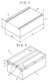
- the marker grooves 2 are cut by using a dicing saw.
- First of all the cutting of the marker grooves 2 in the surface of the Si substrate 1 is carried out in order to facilitate visual confirmation of the positions of the marker grooves 2, because Si has metallic luster, and thereby to permit pin guide grooves and fiber guide grooves to be cut with high accuracy in the subsequent steps.
- a lower cladding 3 of silica glass having a thickness of, e.g., 20 ⁇ m, two channel optical waveguides 4, and an upper cladding 5 of, e.g., 20 ⁇ m thick are successively formed on the surface of the substrate 1, such that the marker grooves 2 are filled up with the lower cladding 3 as shown in FIG. 2, thereby obtaining a waveguide body A.
- photomask alignment is carried out with a submicron accuracy, using the marker grooves 2 as positioning reference.
- each of the channel optical waveguides 4 has a square cross section of, e.g., 8 ⁇ m by 8 ⁇ m, and has a difference in specific refraction index, ⁇ , of 0.3%.
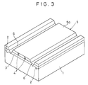
- two V-grooves for example, which extend along the optical axes of the optical waveguides 4, are cut in a surface 5a of the upper cladding 5 by slicing, as shown in FIG. 3, thereby making pin guide grooves 6.
- the pin guide grooves 6 are made after the formation of the upper cladding 5 for the following reason:
- silica glass is deposited on surface and forms a fine particle layer, and this glass particle layer shrinks after the formation of the upper cladding 5.
- the pin guide grooves 6 are formed, thereby stabilizing the dimensional accuracy thereof.
- the waveguide body A with the pin guide grooves 6 formed therein is cut in a direction perpendicular to the optical axes of the waveguides 4, to obtain two end chips B1 and B3 and a central chip B2, as shown in FIG. 4.
- the marker grooves 2, the channel optical waveguides 4, and the pin guide grooves 6 of these chips are respectively aligned along the optical axes, forming two straight marker grooves, two straight waveguides, and two straight pin guide grooves as before the waveguide body A is cut.
- the fiber guide grooves 7 should have a cross sectional shape such that, when optical fibers are placed therein, the fibers are aligned with the corresponding waveguides 4 of the central chip B2.
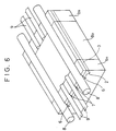
- the fiber aligning jigs b1 and b3 are abutted onto the opposite end faces of the central chip (waveguide chip) B2, whereby the two pin guide grooves 6 of the individual chips are aligned along the optical axes of the waveguides 4.
- a guide pin 8 is laid in each of the V-grooves (pin guide grooves) 6 so as to extend across the central chip B2 and the fiber aligning jigs b1 and b3, and two optical fibers 9 to be connected to the respective channel optical waveguides 4 of the central chip B2 are placed respectively in the two fiber guide grooves 7 of each of the fiber aligning jigs b1 and b3 (FIG. 6).
- a cover 10 which has the similar cross sectional shape as the fiber aligning jigs b1 and b3 and has pin guide grooves 11 and fiber guide grooves 12 formed therein corresponding in position to the pin guide grooves 6 and the fiber guide grooves 7, respectively, as shown in FIG. 7, is placed on the butted structure (b1, B2, b3), whereby the structure (b1, B2, b3) and the cover 10 urgingly hold the guide pins 8 and the optical fibers 9 therebetween.
- the central chip B2 and the fiber aligning jigs b1 and b3 are fixed in position and prevented from being displaced in the transverse direction relative to each other by the guide pins 8 laid along the respective V-grooves (pin guide grooves ) 6, and also the optical fibers 9 placed in the respective fiber guide grooves 7 of the fiber aligning jigs b1 and b3 are fixed in position and aligned with the corresponding channel optical waveguides 4 of the central chip B2.
- the central chip (waveguide chip) B2 and the fiber aligning jigs b1 and b3 are bonded at their butted end faces by an optical adhesive, thereby completing the connection of the optical fibers 9 to the associated channel optical waveguides 4.
- silica glass layers having a total thickness of about 40 ⁇ m are formed on the surface of the 1 mm-thick Si substrate by the flame hydrolysis deposition method, the silica glass layers are subject to warp having a curvature of the order of meters.
- the channel optical waveguide 4 and the optical fibers 9 are actually situated along an arc curved with respect to a horizontal plane.
- each waveguide 4 and the associated optical fibers 9 extend along the same arc, misalignment of the optical axes does not occur.
- the present invention is not limited to such application alone.
- the method according to the present invention can be applied collectively to a plurality of waveguide chips formed on a single wafer.
- pin guide grooves 6 may be cut in each of the chips, using the marker grooves 2 as reference marks. Then, fiber guide grooves 7 are formed in each of the end chips, also using the marker grooves 2 as reference marks.
- the substrate 1 formed with the marker grooves 2 alone, shown in FIG. 1 may be first cut in the width direction to obtain three chips.
- a silica glass layer composed of a lower cladding 3, channel optical waveguides 4, and an upper cladding 5 is formed on the central chip by the flame hydrolysis deposition method, while such a glass layer deposition is not done on the end chips, and then pin guide grooves 6 are formed separately in the individual chips, using the marker grooves 2 as reference marks.
- the distance between the pin guide grooves 6 formed in each end chip serving as the fiber aligning jig must be smaller by about 0.01% than that between the pin guide grooves 6 formed in the central chip serving as the waveguide chip.
- marker grooves 2 may be cut with a predetermined relative position to the core channel.
- the marker grooves 2 are used thereafter as reference marks when forming pin guide grooves 6.
Landscapes
- Physics & Mathematics (AREA)
- General Physics & Mathematics (AREA)
- Optics & Photonics (AREA)
- Optical Couplings Of Light Guides (AREA)
Applications Claiming Priority (2)
| Application Number | Priority Date | Filing Date | Title |
|---|---|---|---|
| JP138789/92 | 1992-05-29 | ||
| JP4138789A JPH05333231A (ja) | 1992-05-29 | 1992-05-29 | 光導波路と光ファイバの接続方法 |
Publications (2)
| Publication Number | Publication Date |
|---|---|
| EP0571924A1 true EP0571924A1 (de) | 1993-12-01 |
| EP0571924B1 EP0571924B1 (de) | 1996-08-21 |
Family
ID=15230255
Family Applications (1)
| Application Number | Title | Priority Date | Filing Date |
|---|---|---|---|
| EP93108363A Expired - Lifetime EP0571924B1 (de) | 1992-05-29 | 1993-05-24 | Verfahren zum Verbinden eines optischen Wellenleiters mit einer optischen Faser |
Country Status (5)
| Country | Link |
|---|---|
| US (1) | US5297228A (de) |
| EP (1) | EP0571924B1 (de) |
| JP (1) | JPH05333231A (de) |
| CA (1) | CA2096894A1 (de) |
| DE (1) | DE69304138T2 (de) |
Cited By (7)
| Publication number | Priority date | Publication date | Assignee | Title |
|---|---|---|---|---|
| EP0670507A1 (de) * | 1994-03-03 | 1995-09-06 | France Telecom | Optisches Mehrweg-Verbindungsverfahren für optische Fasern |
| WO1995025974A1 (en) * | 1994-03-18 | 1995-09-28 | Telefonaktiebolaget Lm Ericsson | Encapsulation of optoelectronic components |
| EP0718649A1 (de) * | 1994-12-23 | 1996-06-26 | ITALTEL SOCIETA ITALIANA TELECOMUNICAZIONI s.p.a. | Selbstjustierendes Kupplungssystem für optische Fasern und Wellenleiter |
| US5715338A (en) * | 1994-03-16 | 1998-02-03 | Telefonaktiebolaget Lm Ericcson | Impermeable encapsulation of optoelectronic components |
| EP1237021A2 (de) * | 2001-02-27 | 2002-09-04 | Ngk Insulators, Ltd. | Substrat für die Montage optischer Komponenten, Herstellungsmethode des Substrats und optische Anordnung unter Verwendung des Substrats |
| EP1353205A2 (de) * | 2002-02-14 | 2003-10-15 | Agilent Technologies Inc. (a Delaware Corporation) | Ausrichtung einer Faseranordnung mit Hilfe von Justagemarkierungen |
| WO2021108235A1 (en) * | 2019-11-30 | 2021-06-03 | Corning Incorporated | Optical waveguides and methods for producing |
Families Citing this family (40)
| Publication number | Priority date | Publication date | Assignee | Title |
|---|---|---|---|---|
| JPH06201936A (ja) * | 1992-12-28 | 1994-07-22 | Matsushita Electric Ind Co Ltd | 光ファイバアレイ及びその製造方法 |
| CA2127861C (en) * | 1993-07-14 | 2004-09-21 | Shinji Ishikawa | Coupling structure of optical fibers and optical waveguides |
| JPH0792342A (ja) * | 1993-07-29 | 1995-04-07 | Sumitomo Electric Ind Ltd | 光導波路モジュール |
| US5400423A (en) * | 1993-09-07 | 1995-03-21 | Motorola | Molded star coupler and method of making same |
| EP1482336A3 (de) | 1994-07-21 | 2004-12-22 | Sumitomo Electric Industries, Ltd. | Optisches Wellenleitermodul mit einem Substrat aus einem bestimmten Material und einem Ferrule aus einem anderen Material |
| US5572614A (en) * | 1994-11-04 | 1996-11-05 | Alcatel Network Systems, Inc. | Method and apparatus for aligning a separately supported fiber tip and fiber communications circuit |
| US5471552A (en) * | 1995-02-22 | 1995-11-28 | Industrial Technology Research Institute | Fabrication of static-alignment fiber-guiding grooves for planar lightwave circuits |
| JP3356581B2 (ja) * | 1995-05-12 | 2002-12-16 | 松下電器産業株式会社 | 光回路部品及びその製造方法 |
| FR2746545B1 (fr) * | 1996-03-25 | 1998-06-12 | Alcatel Sel Aktiengesellsohaft | Procede pour fabriquer un composant a substrat de silicium cristallin |
| US5748827A (en) * | 1996-10-23 | 1998-05-05 | University Of Washington | Two-stage kinematic mount |
| JP3835018B2 (ja) * | 1998-10-26 | 2006-10-18 | 住友電気工業株式会社 | 光デバイスと光デバイスを備えた光モジュール |
| CA2258398A1 (en) * | 1999-01-07 | 2000-07-07 | Victor Benham | An adhesive-free lens-attached optical fibers to optical waveguide packaging system |
| US6595700B2 (en) | 2000-04-04 | 2003-07-22 | Shipley Company, L.L.C. | Optoelectronic packages having insulation layers |
| US6866426B1 (en) * | 2000-04-07 | 2005-03-15 | Shipley Company, L.L.C. | Open face optical fiber array for coupling to integrated optic waveguides and optoelectronic submounts |
| US6848839B2 (en) * | 2000-04-07 | 2005-02-01 | Shipley Company, L.L.C. | Methods and devices for coupling optoelectronic packages |
| US6842552B1 (en) | 2000-04-13 | 2005-01-11 | Shipley Company, L.L.C. | Optical waveguide switch |
| US6832016B2 (en) | 2000-04-13 | 2004-12-14 | Shipley Company, L.L.C. | Fiber array switch having micromachined front face with roller balls |
| US6798933B2 (en) * | 2000-04-14 | 2004-09-28 | Shipley Company, L.L.C. | Fiber optic array switch |
| US6826324B2 (en) * | 2000-04-13 | 2004-11-30 | Shipley Company, L.L.C. | Optical waveguide switch |
| US6847764B2 (en) | 2000-04-14 | 2005-01-25 | Shipley Company, L.L.C. | Optical interconnect having alignment depression |
| US6633691B2 (en) * | 2000-05-02 | 2003-10-14 | Shipley Company, L.L.C. | Optical waveguide switch having stepped waveguide holding member |
| US6748131B2 (en) * | 2000-05-19 | 2004-06-08 | Shipley Company, L.L.C. | Optical waveguide devices and methods of fabricating the same |
| US6788853B2 (en) * | 2000-06-28 | 2004-09-07 | Shipley Company, L.L.C. | Method for cleaving integrated optic waveguides to provide a smooth waveguide endface |
| KR100382704B1 (ko) * | 2000-06-29 | 2003-05-01 | 박찬식 | 광통신용 광도파로 소자 모듈을 구성하기 위한 광섬유의 정렬 방법 |
| US6870981B2 (en) | 2000-08-24 | 2005-03-22 | Shipley Company, L.L.C. | Optical switch and method for making |
| US6853764B2 (en) * | 2000-08-28 | 2005-02-08 | Shipley Company, L.L.C. | Optical switch assembly and method for making |
| US6810162B2 (en) * | 2000-12-20 | 2004-10-26 | Shipley Company, L.L.C. | Optical switch assembly with flex plate and method for making |
| US6986608B2 (en) | 2001-01-16 | 2006-01-17 | Molex Incorporated | Passive alignment connection for fiber optics |
| US6744953B2 (en) * | 2001-09-07 | 2004-06-01 | Agilent Technologies, Inc. | Planar optical waveguide with alignment structure |
| US6631228B2 (en) | 2001-09-14 | 2003-10-07 | Photon-X, Inc. | Adhesive-free bonding method of fiber attachment for polymer optical waveguide on polymer substrate |
| AU2002357700A1 (en) * | 2001-11-08 | 2003-05-19 | Shipley Company, Llc | Fiber optic termination |
| KR100476317B1 (ko) * | 2002-10-24 | 2005-03-16 | 한국전자통신연구원 | 광결합 소자 및 그 제작 방법, 광결합 소자 제작을 위한마스터 및 그 제작 방법 |
| KR100467833B1 (ko) * | 2002-12-24 | 2005-01-25 | 삼성전기주식회사 | 광도파로용 다층 인쇄회로기판을 형성하는 방법 |
| US7076136B1 (en) | 2003-03-11 | 2006-07-11 | Inplane Photonics, Inc. | Method of attaching optical fibers to integrated optic chips that excludes all adhesive from the optical path |
| JP2010128089A (ja) * | 2008-11-26 | 2010-06-10 | Nitto Denko Corp | 光導波路および光学式タッチパネル |
| US10048455B2 (en) * | 2016-01-18 | 2018-08-14 | Cisco Technology, Inc. | Passive fiber array connector alignment to photonic chip |
| US11105989B2 (en) * | 2017-03-29 | 2021-08-31 | Agency For Science, Technology And Research | Optical assembly and method of forming the same |
| US10656339B2 (en) | 2018-03-14 | 2020-05-19 | Cisco Technology, Inc. | Fiber to chip alignment using passive vgroove structures |
| JP7043999B2 (ja) * | 2018-07-11 | 2022-03-30 | 日本電信電話株式会社 | ハイブリッド光デバイスの溝作製方法およびハイブリッド光デバイス |
| US11145606B1 (en) * | 2020-03-26 | 2021-10-12 | Globalfoundries U.S. Inc. | Corner structures for an optical fiber groove |
Citations (1)
| Publication number | Priority date | Publication date | Assignee | Title |
|---|---|---|---|---|
| WO1992021047A1 (en) * | 1991-05-20 | 1992-11-26 | The Furukawa Electric Co., Ltd. | Method of connecting optical waveguide to optical fiber |
Family Cites Families (4)
| Publication number | Priority date | Publication date | Assignee | Title |
|---|---|---|---|---|
| CH628152A5 (fr) * | 1977-11-24 | 1982-02-15 | Comp Generale Electricite | Fiche de connecteur fibre a fibre pour cable optique multifibre. |
| US5018817A (en) * | 1987-07-24 | 1991-05-28 | Brother Kogyo Kabushiki Kaisha | Method of optically coupling optical fiber to waveguide on substrate, and optical device produced by the method |
| US4904036A (en) * | 1988-03-03 | 1990-02-27 | American Telephone And Telegraph Company, At&T Bell Laboratories | Subassemblies for optoelectronic hybrid integrated circuits |
| FR2661516B1 (fr) * | 1990-04-27 | 1992-06-12 | Alcatel Fibres Optiques | Composant d'optique integree et procede de fabrication. |
-
1992
- 1992-05-29 JP JP4138789A patent/JPH05333231A/ja active Pending
-
1993
- 1993-05-17 US US08/063,005 patent/US5297228A/en not_active Expired - Fee Related
- 1993-05-24 DE DE69304138T patent/DE69304138T2/de not_active Expired - Fee Related
- 1993-05-24 EP EP93108363A patent/EP0571924B1/de not_active Expired - Lifetime
- 1993-05-25 CA CA002096894A patent/CA2096894A1/en not_active Abandoned
Patent Citations (1)
| Publication number | Priority date | Publication date | Assignee | Title |
|---|---|---|---|---|
| WO1992021047A1 (en) * | 1991-05-20 | 1992-11-26 | The Furukawa Electric Co., Ltd. | Method of connecting optical waveguide to optical fiber |
Non-Patent Citations (3)
| Title |
|---|
| PATENT ABSTRACTS OF JAPAN vol. 14, no. 158 (P-1027)18 January 1990 & JP-A-02 015 204 ( NTT ) * |
| PATENT ABSTRACTS OF JAPAN vol. 14, no. 349 (P-1084)14 May 1990 & JP-A-02 125 209 ( SUMITOMO ELECTRIC ) * |
| PATENT ABSTRACTS OF JAPAN vol. 16, no. 393 (P-1406)30 April 1992 & JP-A-04 128 809 ( FURUKAWA ELECTRIC ) * |
Cited By (12)
| Publication number | Priority date | Publication date | Assignee | Title |
|---|---|---|---|---|
| EP0670507A1 (de) * | 1994-03-03 | 1995-09-06 | France Telecom | Optisches Mehrweg-Verbindungsverfahren für optische Fasern |
| FR2716981A1 (fr) * | 1994-03-03 | 1995-09-08 | Boscher Daniel | Procédé de connexion optique multivoies pour fibres optiques. |
| US5596662A (en) * | 1994-03-03 | 1997-01-21 | France Telecom | Multichannel optical connection method for optical fibers |
| US5715338A (en) * | 1994-03-16 | 1998-02-03 | Telefonaktiebolaget Lm Ericcson | Impermeable encapsulation of optoelectronic components |
| WO1995025974A1 (en) * | 1994-03-18 | 1995-09-28 | Telefonaktiebolaget Lm Ericsson | Encapsulation of optoelectronic components |
| US5818990A (en) * | 1994-03-18 | 1998-10-06 | Telefonaktiebolaget Lm Ericsson | Encapsulation of optoelectronic components |
| EP0718649A1 (de) * | 1994-12-23 | 1996-06-26 | ITALTEL SOCIETA ITALIANA TELECOMUNICAZIONI s.p.a. | Selbstjustierendes Kupplungssystem für optische Fasern und Wellenleiter |
| EP1237021A2 (de) * | 2001-02-27 | 2002-09-04 | Ngk Insulators, Ltd. | Substrat für die Montage optischer Komponenten, Herstellungsmethode des Substrats und optische Anordnung unter Verwendung des Substrats |
| EP1237021A3 (de) * | 2001-02-27 | 2004-04-14 | Ngk Insulators, Ltd. | Substrat für die Montage optischer Komponenten, Herstellungsmethode des Substrats und optische Anordnung unter Verwendung des Substrats |
| EP1353205A2 (de) * | 2002-02-14 | 2003-10-15 | Agilent Technologies Inc. (a Delaware Corporation) | Ausrichtung einer Faseranordnung mit Hilfe von Justagemarkierungen |
| EP1353205A3 (de) * | 2002-02-14 | 2004-06-09 | Agilent Technologies Inc. (a Delaware Corporation) | Ausrichtung einer Faseranordnung mit Hilfe von Justagemarkierungen |
| WO2021108235A1 (en) * | 2019-11-30 | 2021-06-03 | Corning Incorporated | Optical waveguides and methods for producing |
Also Published As
| Publication number | Publication date |
|---|---|
| CA2096894A1 (en) | 1993-11-30 |
| DE69304138T2 (de) | 1997-04-03 |
| JPH05333231A (ja) | 1993-12-17 |
| US5297228A (en) | 1994-03-22 |
| EP0571924B1 (de) | 1996-08-21 |
| DE69304138D1 (de) | 1996-09-26 |
Similar Documents
| Publication | Publication Date | Title |
|---|---|---|
| US5297228A (en) | Method of connecting an optical fiber to an optical waveguide | |
| KR960014123B1 (ko) | 광도파로와 광파이버의 접속방법 | |
| US6099684A (en) | Procedure for assembling the ends of optical fibers into a sheet | |
| US5471552A (en) | Fabrication of static-alignment fiber-guiding grooves for planar lightwave circuits | |
| US4979970A (en) | Method of manufacturing integrated optical component | |
| US5218663A (en) | Optical waveguide device and method for connecting optical waveguide and optical fiber using the optical waveguide device | |
| US6647184B2 (en) | Optical waveguide device and method of manufacturing the same | |
| US5123068A (en) | Integrated optical component and method of manufacture | |
| US4943130A (en) | Integrated optical component | |
| JP3273490B2 (ja) | 多芯マイクロキャピラリとこれを用いた光導波回路と光ファイバとの接続方法 | |
| US20020076189A1 (en) | Method for preparing optical fibers for connection to other fibers or to planar waveguides and device for such connection | |
| JP2550890B2 (ja) | 光導波路の接続構造およびその製造方法 | |
| KR100357853B1 (ko) | 랜드 마크를 이용한 평면 광도파로 소자 | |
| JP2771167B2 (ja) | 光集積回路の実装方法 | |
| JPH05181036A (ja) | 光集積要素を有する光学装置及び製造方法 | |
| JPH09230167A (ja) | 光ガイドの接続構造 | |
| JP3026477B2 (ja) | 光導波路基板 | |
| WO2002061479A1 (fr) | Reseau de fibres optiques et procede de connexion de circuits a l'aide d'un tel reseau de fibres optiques | |
| JPH10133041A (ja) | フィルタ付導波路 | |
| JP3243021B2 (ja) | 光導波路素子の作製方法 | |
| JP3138516B2 (ja) | 光機能素子結合部材およびその製造方法 | |
| JPH0720358A (ja) | 光ファイバ付平面導光路部品およびその製造方法 | |
| JPH11183750A (ja) | 光デバイス用光導波路モジュールおよび光デバイスの製造方法 | |
| JP2003227962A (ja) | 光導波路モジュール | |
| EP1302795A1 (de) | Vorrichtung und Verfahren zum Verbinden einer optischen Faser mit einem optischen Wellenleiter |
Legal Events
| Date | Code | Title | Description |
|---|---|---|---|
| PUAI | Public reference made under article 153(3) epc to a published international application that has entered the european phase |
Free format text: ORIGINAL CODE: 0009012 |
|
| AK | Designated contracting states |
Kind code of ref document: A1 Designated state(s): DE FR GB |
|
| 17P | Request for examination filed |
Effective date: 19940511 |
|
| 17Q | First examination report despatched |
Effective date: 19950425 |
|
| GRAH | Despatch of communication of intention to grant a patent |
Free format text: ORIGINAL CODE: EPIDOS IGRA |
|
| GRAA | (expected) grant |
Free format text: ORIGINAL CODE: 0009210 |
|
| AK | Designated contracting states |
Kind code of ref document: B1 Designated state(s): DE FR GB |
|
| ET | Fr: translation filed | ||
| REF | Corresponds to: |
Ref document number: 69304138 Country of ref document: DE Date of ref document: 19960926 |
|
| PLBE | No opposition filed within time limit |
Free format text: ORIGINAL CODE: 0009261 |
|
| STAA | Information on the status of an ep patent application or granted ep patent |
Free format text: STATUS: NO OPPOSITION FILED WITHIN TIME LIMIT |
|
| 26N | No opposition filed | ||
| PGFP | Annual fee paid to national office [announced via postgrant information from national office to epo] |
Ref country code: FR Payment date: 19980511 Year of fee payment: 6 |
|
| PGFP | Annual fee paid to national office [announced via postgrant information from national office to epo] |
Ref country code: GB Payment date: 19980515 Year of fee payment: 6 |
|
| PGFP | Annual fee paid to national office [announced via postgrant information from national office to epo] |
Ref country code: DE Payment date: 19980529 Year of fee payment: 6 |
|
| PG25 | Lapsed in a contracting state [announced via postgrant information from national office to epo] |
Ref country code: GB Free format text: LAPSE BECAUSE OF NON-PAYMENT OF DUE FEES Effective date: 19990524 |
|
| GBPC | Gb: european patent ceased through non-payment of renewal fee |
Effective date: 19990524 |
|
| PG25 | Lapsed in a contracting state [announced via postgrant information from national office to epo] |
Ref country code: FR Free format text: LAPSE BECAUSE OF NON-PAYMENT OF DUE FEES Effective date: 20000131 |
|
| PG25 | Lapsed in a contracting state [announced via postgrant information from national office to epo] |
Ref country code: DE Free format text: LAPSE BECAUSE OF NON-PAYMENT OF DUE FEES Effective date: 20000301 |
|
| REG | Reference to a national code |
Ref country code: FR Ref legal event code: ST |