EP0552803B1 - Halftone image recording device - Google Patents
Halftone image recording device Download PDFInfo
- Publication number
- EP0552803B1 EP0552803B1 EP93100998A EP93100998A EP0552803B1 EP 0552803 B1 EP0552803 B1 EP 0552803B1 EP 93100998 A EP93100998 A EP 93100998A EP 93100998 A EP93100998 A EP 93100998A EP 0552803 B1 EP0552803 B1 EP 0552803B1
- Authority
- EP
- European Patent Office
- Prior art keywords
- pulse width
- waveform
- voltage
- ion
- pulse
- Prior art date
- Legal status (The legal status is an assumption and is not a legal conclusion. Google has not performed a legal analysis and makes no representation as to the accuracy of the status listed.)
- Expired - Lifetime
Links
- 238000006243 chemical reaction Methods 0.000 claims description 16
- 150000002500 ions Chemical class 0.000 description 51
- 230000005684 electric field Effects 0.000 description 12
- 239000003990 capacitor Substances 0.000 description 8
- 239000012212 insulator Substances 0.000 description 8
- 239000007787 solid Substances 0.000 description 6
- 230000003321 amplification Effects 0.000 description 3
- 238000010586 diagram Methods 0.000 description 3
- 238000003199 nucleic acid amplification method Methods 0.000 description 3
- 230000000295 complement effect Effects 0.000 description 2
- 238000007599 discharging Methods 0.000 description 2
- 238000000034 method Methods 0.000 description 2
- 238000004088 simulation Methods 0.000 description 2
- 230000001133 acceleration Effects 0.000 description 1
- 230000015572 biosynthetic process Effects 0.000 description 1
- 230000003247 decreasing effect Effects 0.000 description 1
- 230000002349 favourable effect Effects 0.000 description 1
- 230000010363 phase shift Effects 0.000 description 1
- 239000004065 semiconductor Substances 0.000 description 1
- 238000003079 width control Methods 0.000 description 1
Images


Classifications
-
- H—ELECTRICITY
- H04—ELECTRIC COMMUNICATION TECHNIQUE
- H04N—PICTORIAL COMMUNICATION, e.g. TELEVISION
- H04N1/00—Scanning, transmission or reproduction of documents or the like, e.g. facsimile transmission; Details thereof
- H04N1/40—Picture signal circuits
- H04N1/40025—Circuits exciting or modulating particular heads for reproducing continuous tone value scales
- H04N1/40043—Circuits exciting or modulating particular heads for reproducing continuous tone value scales using more than one type of modulation, e.g. pulse width modulation and amplitude modulation
-
- H—ELECTRICITY
- H04—ELECTRIC COMMUNICATION TECHNIQUE
- H04N—PICTORIAL COMMUNICATION, e.g. TELEVISION
- H04N1/00—Scanning, transmission or reproduction of documents or the like, e.g. facsimile transmission; Details thereof
- H04N1/40—Picture signal circuits
- H04N1/40056—Circuits for driving or energising particular reading heads or original illumination means
-
- H—ELECTRICITY
- H04—ELECTRIC COMMUNICATION TECHNIQUE
- H04N—PICTORIAL COMMUNICATION, e.g. TELEVISION
- H04N1/00—Scanning, transmission or reproduction of documents or the like, e.g. facsimile transmission; Details thereof
- H04N1/40—Picture signal circuits
- H04N1/40081—Soft dot halftoning, i.e. producing halftone dots with gradual edges
Definitions
- the present invention relates to halftone image recording hardware for controlling a charge flow such as an ion flow for recording halftone images and to a high voltage-resistant circuit that enables such recording hardware to work at high speed.
- a slit control type of image recorder harnessing corotron discharge in which ions generated by corotron discharge are introduced in a slit and the resulting ion flow is controlled by varying an electric field within the slit wall to form a charge pattern on a recording medium
- an aperture control type of image recorder making use of corotron discharge in which ions generated by corotron are passed through apertures in two control electrodes while controlling an electric field between them, and the resulting ion flow that goes toward a recording medium is placed under on-off control to form a charge pattern on the recording medium
- an aperture control type of image recorder harnessing solid discharge in which high-frequency voltage is applied between electrodes with an insulator located between them to induce discharge and the resulting ions are selectively drawn by electric field control to form a charge pattern on a recording medium.
- the ion flow is constricted by reducing the magnitude of the electric field between the ion flow-control electrodes, making the resulting dot diameter small and, at the same time, giving rise to dot density variations.
- the magnitude of the electric field between the electrodes controlling the ion flow increases, there is an increase in the diameter of the ion flow, which concurs with dot density variations. In either case, it is possible to form halftone images by inter-electrode field control.
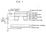
- Fig. 1 is a representation for illustrating an aperture control type of image recorder that makes use of solid discharge and is driven by alternating currents.
- a recording head shown generally at 1 is built up of a line electrode 1b and an insulator 1c stacked on an insulator 1a in this order.
- a central aperture is defined by a finger electrode 1d, an insulator 1e and a screen electrode 1f, and a high-frequency power source 5 is connected between the line and finger electrodes 1b and 1d.
- a signal source 6 is connected between the finger and screen electrodes 1d and 1f for the application of signal voltage.
- An insulating, recording member 2 provided with an electrode 3 is located in opposition to the recording head 1, and a direct-current power source E is connected between the recording head 1 and the recording member for ion flow acceleration.
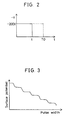
- This image recorder works as follows. Ion generation is induced by intra-head discharge caused by the application of a high-frequency voltage of a few KV to a few MHz between the line and finger electrodes 1b and 1d. A flow of the resulting ions is controlled in dependence on signal voltage between the finger and screen electrodes 1d and 1f. This signal voltage or, in other words, a pulse width modulation signal is then varied in terms of width t in dependence on signal strength, as shown in Fig. 2 with TO representing the maximum signal width, whereby an electrostatic latent image having halftones is formed on the recording member.
- a voltage amplifier circuit of high input impedance and excellent in linearity is usually used so as to amplify halftone image data to a predetermined voltage, and a variety of D-A converters such as those of the resistance and integral types are used as well.
- the D-A converters when built up of ICs, unexceptionally produce only low-voltage output. In addition, when it is intended to set up discrete circuits, such problems as mentioned above arise, usually because of the need of using a voltage amplifier circuit.
- Conventional or ordinary D-A converters because of being designed to obtain a continuos form of output, do not lend themselves well for ion printers, plasma displays, and so on, for which a discrete, high-voltage rectangular waveform of pulses must be produced.
- circuits for driving ion printers, plasma displays, and so on are presumed to work in the form of a parallel array of many identical circuits. To achieve this, however, lower power and lower cost are needed.
- driving circuits with built-in FETs are available for driving ion printers, etc.
- Fig. 5 is an illustration of a typical driving circuit using a complementary FET.
- an N-channel FET 11 and a P-channel FET 12 are connected in series, and 0 V and 15 V, for instance, are added to this series circuit as gate input.
- a level shifter 13 Connected to the gate of P-channel FET 12 is a level shifter 13 for converting 0 or 15 V to the on-off control signal level of P-channel FET 12. Then, 0 V and 15 V are alternately fed to the gates of N-channel FET 11 and P-channel FET 12 to put them on and off to achieve low and high-level outputs.
- Fig. 6 is an illustration of a typical driving circuit using resistance loading. As illustrated in Fig. 6(a), a resistance R is connected to the drain side of an N-channel FET 14. At a gate input of 15 V, FET 14 is put on to produce nothing, whereas at a gate input of 0 V, FET 14 is put off to produce low- and high-level outputs.
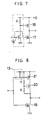
- Fig. 7 is a typical representation of a totem pole combination of N-channel FETs, in which a buffer is provided to a resistance load type of circuit shown by a broken line in Fig. 7(a). With this circuit, it is possible to obtain a large output current by a buffer 18 and to achieve a sharp rise as well.
- Fig. 8 is an illustration of a typical high voltage-resistant driving circuit built up of a series combination of low voltage-resistant P-channel FETs 20 and 21.
- This circuit is designed to work such that putting P-channel FET 21 off causes P-channel FET 20 to be off, and putting P-channel FET 21 on gives rise to putting P-channel FET 20 on.
- This circuit is allowed to withstand high voltage because of a series combination of P-channel FETs 20 and 21.
- Illustrated in Fig. 5 is a basic driving circuit, but this is unsuitable for a high-voltage driving circuit, because much difficulty is now involved in procuring P-channel FETs having a voltage resistance of 300 V or higher.
- the circuit of Fig. 6 can work at high speed and at a short output waveform fall time, but its rise characteristics are generally not well, because it depends on the value of resistance R and output load, as shown in Fig. 6(b).
- R resistance
- N-channel FET 14 is put on, resulting in a power consumption increase.
- the circuit of Fig. 7 is favorable for large capacity loading, but a similar problem as in the resistance loading type circuit of Fig. 6 arises under a capacitive load almost similar to the gate input capacity of an FET. In short, the value of resistance R must be reduced so as to allow N-channel FET 17 to work at high speed, but this results in a power consumption increase.
- the circuit of Fig. 8 may be made high-resistant to voltage, because of being built up of a series combination of P-channel FETs, but it cannot work at high speed due to a time constant ascribable to resistance R and the capacities of the FETs.
- R When the value of R is reduced so as to achieve high-speed performance, there is a current increase when N-channel FET 19 is put on, as in the circuit of Fig. 6, only to give rise to a power consumption increase.
- US-A-4,679,057 discloses an electrophotographic apparatus, in which a laser beam modulated by an image signal is irradiated to a photosensitive member to form an electrostatic latent image and a toner image is obtained. Gradation is provided by simultaneously performing pulse width-modulation and amplitude-modulation.
- EP-A-0,451,770 discloses an electrophotographic apparatus, in which a laser beam modulated by an image signal is irradiated on a photosensitive member to form an electrostatic latent image, and a toner image is obtained.
- the amplitude-modulation is performed on a triangular wave with a density signal, and a semiconductor laser is driven by a modulation signal; the photosensitive member is irradiated.
- An electrostatic latent image is formed by attenuating the potential on the photosensitive member by the intensity of the irradiated light.
- JP-60-219,071 shows the waveform of an ion current generated from the corona wire.
- An object of the invention is to provide a halftone image recorder apparatus that makes good-quality halftone reproduction feasible.
- Another object of the invention is to provide an aperture control type of image recorder apparatus by alternating-current driven solid discharge, which can be used to smooth a surface potential change in a recording member with respect to pulse width, thereby achieving good-quality halftone reproduction.
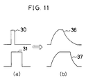
- This embodiment is characterized by imparting a time constant to at least one of the leading and trailing edges of a pulse width-modulated signal applied to a recording head.
- signals 30 and 31 that are pulse-widthwise modulated in correspondence to image signals are converted to signals 32 and 33 of a waveform with a time constant imparted to the trailing edge through a waveform conversion circuit to be described later, as illustrated in Fig. 9.
- signals 30 and 31 that are pulse-widthwise modulated in correspondence to image signals are converted to signals 34 and 35 of a waveform with a time constant imparted to the leading edge
- signals 30 and 31 that are pulse-widthwise modulated in correspondence to image signals are converted to signals 36 and 37 of a waveform with time constants imparted to the trailing and leading edges.
- Waveform conversion circuit 40 is built up of switches S1 and S2, a resistance R1 and a capacitor C, and is designed such that switches S1 and S2 are respectively closed and opened at a pulse rise time to apply a pulse voltage to capacitor C, and switches S1 and S2 are respectively opened and closed at a pulse fall time for discharge by a time constant circuit defined by capacitor C and resistance R1. It is noted that this may be achieved by the mere application of the point of contact of switch S1 with resistance R1 to the electrode of the recording head.
- Waveform signals of Fig. 10 are obtained by a waveform conversion circuit 41 shown in Fig. 12(b).
- switches S1 and S2 are respectively closed and opened at a pulse rise time, so that a time constant can be obtained by a time constant circuit comprising resistance R1 and capacitor C.
- switches S1 and S2 are respectively opened and closed, so that capacitor C can be short-circuited and so is instantaneously discharged and then drops to ground potential.
- Waveform signals 36 and 37 of Fig. 11 are obtained by a waveform conversion circuit 42.
- switches S1 and S2 are respectively closed and opened at a pulse rise time, so that a time constant can be provided by a charging curve due to a time constant circuit comprising resistance R2 and capacitor C
- switches S1 and S2 are respectively opened and closed, so that a time constant can be provided by a charging curve due to a time constant circuit comprising capacitor C and resistances R1 and R2.
- the driving waveforms of the instant embodiment are not limited to those having such time constants as shown in Figs. 9-11; in other words, they may go up or down linearly.
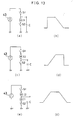
- the resistance in the conversion circuit shown in Fig. 12 is replaced with a constant-current circuit, it is then possible to obtain such a trapezoidal waveform as shown in Fig. 13.
- Fig. 13(a) represents an arrangement in which a constant-current circuit I1 is built in the discharge circuit, thereby obtaining a linearly going-down waveform such as on shown in Fig. 13(b).
- Fig. 13(c) represents an arrangement wherein a constant-current circuit I2 is incorporated in the charging circuit, thereby obtaining a linearly going-up waveform such as one shown in Fig. 13(d).
- Fig. 13(e) illustrates an arrangement wherein constant-current circuits are built in the charging and discharging circuits, thereby obtaining a waveform that goes up linearly and, after a constant voltage is reached, goes down linearly, such as one shown in Fig. 13(f).
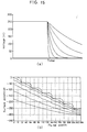
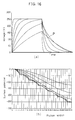
- Fig. 16(a) represents the case where time constants are imparted to the leading and trailing edges of a rectangular wave.
- a waveform P In the case of a waveform P, there is obtained a triangular wave that has an increased time constant but is free from any constant-voltage part.
- Fig. 16(b) there is a stepwise change of surface potential with respect to pulse width as long as the time constant is small, but that surface potential changes smoothly, as the wave approximates to a triangular waveform with increases in the time constants imparted to the leading and trailing edges.
- Fig. 19 represents one embodiment of a pulse width- and amplitude-modulated signal. It is noted that this embodiment is applicable to every ion flow control type of image recorder.
- the amplitude of a pulse having a unit time duration t 0 in correspondence to the input signal voltage is now changed to an amplitude V at a unit amplitude step v.
- a pulse having a time duration t 0 and an amplitude V is shifted in phase by unit time duration t 0 , as shown in Fig. 19(b).
- the pulse having unit time duration t 0 is likewise changed to amplitude V.
- a pulse having a time duration 2t 0 and amplitude V is shifted in phase by unit time duration t 0 , as shown in Fig. 19(c).
- the pulse having unit time duration t 0 is similarly changed to amplitude V.
- phase shift is done by unit time duration t 0 .
- the pulse having unit time duration t 0 is similarly changed to amplitude V at unit amplitude step v.
- amplitude modulation is done with a pulse having unit time duration t 0 at step v, while pulse width modulation is carried out using time duration t 0 as the unit; amplitude and pulse width modulations are done independently from each other.
- the driving speed is determined by either N or M, although the chosen N or M must be larger than the other.
- M M ⁇ N
- the driving speed can be increased to 16 times as large.
- the amplitude of the pulse having unit time duration t 0 be changed to amplitude V at unit amplitude step v, corresponding to the input signal voltage.
- a pulse having time duration t 0 and amplitude V is shifted in phase by time duration t 0 , as shown in Fig. 20(b).
- the pulse having unit time period t 0 is likewise changed in the same phase to amplitude V at unit amplitude step v.
- a pulse having a time duration 2t 0 and amplitude V is shifted in phase by time duration t 0 , as shown in Fig. 20(c).
- the pulse is changed in the same phase to amplitude V at unit amplitude step v.
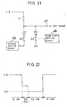
- Fig. 21 illustrates the waveform conversion circuit for generating the pulse waveform shown in Fig. 20, and Fig. 22 is a representation of how the waveform conversion circuit works.
- reference numeral 45 stands for a voltage setting block, 46 a pulse width setting block, 47 an input terminal, and S1-S3 switches.
- the voltage setting block produces at a given unit step a plurality of varying voltages that correspond to the number of halftones.
- the pulse width setting block produces a plurality of pulses having varying widths at a given unit time duration step.
- switches S2 and S3 under switching control at the unit time duration and at the unit time duration or a time duration that is an integral multiple thereof. It is then possible to achieve high-speed driving and high-contrast expression by applying such a modulated pulse through output terminal 47 to an ion head.
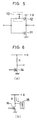
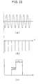
- ion flows are detectable only at the peak of the high-frequency voltage, as already explained in connection with Fig. 4 and as illustrated in Fig. 23(b). To put it another way, they are discretely generated at a certain period and so there is a variation in the quantity of the ions generated.
- the unit time duration t 0 explained with reference to Figs. 19 and 20 corresponds to one ion-generation cycle or cycles that are an integral multiple thereof, it is then possible to generate ion flows in association with a pulse width change.
- the instant embodiment because of making high halftone control easy even when it is driven at high speed, enables printing speed to be increased and good-quality halftone reproduction to be carried out.
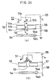
- a corotron type of ion printer shown in Fig. 24 as an example, can be placed under halftone control only by pulse width modulation, because of the constant emission of ions.
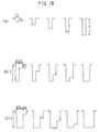
- Figs. 24(a) and (b) provide a conceptional representation of such a corotron type of ion printer, wherein reference numeral 51 stands for a corona ion-generation source, 52 an ion head, 52a an upper aperture electrode, 52b an insulating layer, 52c a lower aperture electrode, 53 a hole, 54 a recording medium, 54a an insulator, 54b an electrically conductive layer, 55 a corona ion-generating power source, 56 and 57 control signal power sources, and 58 a bias electrode.
- reference numeral 51 stands for a corona ion-generation source
- 52a ion head 52a an upper aperture electrode
- 52b an insulating layer
- 52c a lower aperture electrode
- 53 a hole
- 54 a recording medium 54a an insulator
- 54b an electrically conductive layer
- 55 a corona ion-generating power source
- 56 and 57 control signal power sources and 58 a bias electrode.
- Corona ion-generating power source 51 may be built up of a casing electrode 51a and a corona wire 51b laid on in it..
- a direct-current high voltage is applied by corona ion-generating power source 55 between casing electrode 51a and corona wire 51b to generate corona ions.
- Upper and lower aperture electrodes 52a and 52c formed on both sides of insulating layer 52b are provided with a through-aperture that corresponds to hole 53 provided through insulating layer 52b to define a unit recording element, and serves to place an ion flow under on/off control in dependence on the polarity of the control signal voltage applied through control signal power sources 56 and 57.
- corona ions that have passed through the hole in the insulating layer are guided by an electric field made between the insulating layer and conductive layer 5 of recording medium 4b by bias power source 58, thereby forming a latent image on the insulator 54a of recording medium 54.
- signal voltage is furnished to lower electrode 52, as shown in Fig. 24(a), to make upper aperture electrode 52a so positive that a corona ion flow can go onto recording medium 54 along an electric field formed in the electrode aperture to form a latent image on insulator 54a.
- signal voltage is applied such that the polarity of the signal power source is reversed, as shown in Fig. 24(b), an electric field is formed within the electrode aperture in the direction that prevents any ion flow, and so the ions cannot pass through the aperture.
Landscapes
- Engineering & Computer Science (AREA)
- Multimedia (AREA)
- Signal Processing (AREA)
- Printers Or Recording Devices Using Electromagnetic And Radiation Means (AREA)
- Electrophotography Using Other Than Carlson'S Method (AREA)
- Dot-Matrix Printers And Others (AREA)
Priority Applications (1)
| Application Number | Priority Date | Filing Date | Title |
|---|---|---|---|
| EP99120972A EP0982928A3 (en) | 1992-01-22 | 1993-01-22 | Halftone image device and its driving circuit |
Applications Claiming Priority (12)
| Application Number | Priority Date | Filing Date | Title |
|---|---|---|---|
| JP9259/92 | 1992-01-22 | ||
| JP925992A JPH05197242A (ja) | 1992-01-22 | 1992-01-22 | 階調画像記録装置 |
| JP925992 | 1992-01-22 | ||
| JP134912/92 | 1992-05-27 | ||
| JP13491292A JPH05323733A (ja) | 1992-05-27 | 1992-05-27 | イオン流制御方式の階調画像記録装置 |
| JP13491292 | 1992-05-27 | ||
| JP145806/92 | 1992-06-05 | ||
| JP14580692 | 1992-06-05 | ||
| JP14580692 | 1992-06-05 | ||
| JP208974/92 | 1992-08-05 | ||
| JP20897492A JP3181387B2 (ja) | 1992-08-05 | 1992-08-05 | 容量性負荷用高耐圧駆動回路 |
| JP20897492 | 1992-08-05 |
Related Child Applications (1)
| Application Number | Title | Priority Date | Filing Date |
|---|---|---|---|
| EP99120972A Division EP0982928A3 (en) | 1992-01-22 | 1993-01-22 | Halftone image device and its driving circuit |
Publications (3)
| Publication Number | Publication Date |
|---|---|
| EP0552803A2 EP0552803A2 (en) | 1993-07-28 |
| EP0552803A3 EP0552803A3 (enExample) | 1994-02-16 |
| EP0552803B1 true EP0552803B1 (en) | 2000-09-06 |
Family
ID=27455131
Family Applications (2)
| Application Number | Title | Priority Date | Filing Date |
|---|---|---|---|
| EP93100998A Expired - Lifetime EP0552803B1 (en) | 1992-01-22 | 1993-01-22 | Halftone image recording device |
| EP99120972A Withdrawn EP0982928A3 (en) | 1992-01-22 | 1993-01-22 | Halftone image device and its driving circuit |
Family Applications After (1)
| Application Number | Title | Priority Date | Filing Date |
|---|---|---|---|
| EP99120972A Withdrawn EP0982928A3 (en) | 1992-01-22 | 1993-01-22 | Halftone image device and its driving circuit |
Country Status (4)
| Country | Link |
|---|---|
| US (2) | US5687001A (enExample) |
| EP (2) | EP0552803B1 (enExample) |
| CA (1) | CA2087885C (enExample) |
| DE (1) | DE69329350T2 (enExample) |
Families Citing this family (7)
| Publication number | Priority date | Publication date | Assignee | Title |
|---|---|---|---|---|
| EP0851316B1 (en) * | 1996-12-23 | 2002-03-27 | Agfa-Gevaert | Printer and printing method |
| JP2001013912A (ja) * | 1999-06-30 | 2001-01-19 | Fujitsu Ltd | 容量性負荷の駆動方法及び駆動回路 |
| US6404451B1 (en) * | 2000-11-29 | 2002-06-11 | Xerox Corporation | Adjustable voltage finger driver |
| US6417875B1 (en) * | 2000-11-29 | 2002-07-09 | Xerox Corporation | Adjustable voltage finger driver |
| CN2629069Y (zh) * | 2002-03-29 | 2004-07-28 | 精工爱普生株式会社 | 写入头和使用它的图像形成装置 |
| JP4480341B2 (ja) * | 2003-04-10 | 2010-06-16 | 日立プラズマディスプレイ株式会社 | プラズマディスプレイ装置 |
| US7206547B2 (en) * | 2003-09-30 | 2007-04-17 | Elektrobit Oy | Method of testing electric circuit, and arrangement |
Family Cites Families (17)
| Publication number | Priority date | Publication date | Assignee | Title |
|---|---|---|---|---|
| US4149183A (en) * | 1976-05-21 | 1979-04-10 | Xerox Corporation | Electronic halftone generator |
| US4070600A (en) * | 1976-12-23 | 1978-01-24 | General Electric Company | High voltage driver circuit |
| JPS54134547A (en) * | 1978-04-11 | 1979-10-19 | Sony Corp | Mosfet switching circuit |
| JPS60175062A (ja) | 1984-02-21 | 1985-09-09 | Nippon Telegr & Teleph Corp <Ntt> | イオン流制御階調記録方法 |
| JPS60219071A (ja) * | 1984-04-14 | 1985-11-01 | Nippon Telegr & Teleph Corp <Ntt> | イオン流制御階調記録方法 |
| US4679057A (en) * | 1984-11-22 | 1987-07-07 | Minolta Camera Kabushiki Kaisha | Laser recording apparatus |
| JPS61154313A (ja) * | 1984-12-27 | 1986-07-14 | Seikosha Co Ltd | 出力インバ−タの貫通電流防止回路 |
| JPS61228771A (ja) * | 1985-04-02 | 1986-10-11 | Canon Inc | 画像記録装置 |
| US4803384A (en) * | 1985-10-22 | 1989-02-07 | Fujitsu Limited | Pulse amplifier suitable for use in the semiconductor laser driving device |
| JP2505756B2 (ja) * | 1986-07-22 | 1996-06-12 | キヤノン株式会社 | 光学変調素子の駆動法 |
| US4841313A (en) * | 1987-06-16 | 1989-06-20 | Delphax Systems | RF driver and control |
| US4899344A (en) * | 1987-12-07 | 1990-02-06 | Ricoh Co., Ltd. | Semiconductor laser control apparatus |
| JPH01209813A (ja) * | 1988-02-17 | 1989-08-23 | Nec Ic Microcomput Syst Ltd | 出力バッファ回路 |
| DE3856011T2 (de) * | 1988-06-07 | 1998-03-12 | Sharp Kk | Verfahren und Einrichtung zum Steuern eines kapazitiven Anzeigegeräts |
| JPH02162824A (ja) * | 1988-12-16 | 1990-06-22 | Hitachi Ltd | 半導体集積回路装置 |
| US5172132A (en) * | 1990-03-06 | 1992-12-15 | Konica Corporation | Digital image forming device and method for forming an image from a plurality of dots |
| US4992807A (en) * | 1990-05-04 | 1991-02-12 | Delphax Systems | Gray scale printhead system |
-
1993
- 1993-01-21 US US08/007,143 patent/US5687001A/en not_active Expired - Fee Related
- 1993-01-22 EP EP93100998A patent/EP0552803B1/en not_active Expired - Lifetime
- 1993-01-22 DE DE69329350T patent/DE69329350T2/de not_active Expired - Fee Related
- 1993-01-22 CA CA002087885A patent/CA2087885C/en not_active Expired - Fee Related
- 1993-01-22 EP EP99120972A patent/EP0982928A3/en not_active Withdrawn
-
1995
- 1995-04-11 US US08/420,308 patent/US5541542A/en not_active Expired - Fee Related
Also Published As
| Publication number | Publication date |
|---|---|
| US5541542A (en) | 1996-07-30 |
| EP0552803A3 (enExample) | 1994-02-16 |
| US5687001A (en) | 1997-11-11 |
| CA2087885C (en) | 2003-10-28 |
| DE69329350T2 (de) | 2001-05-31 |
| EP0982928A3 (en) | 2000-03-08 |
| CA2087885A1 (en) | 1993-07-23 |
| DE69329350D1 (de) | 2000-10-12 |
| EP0982928A2 (en) | 2000-03-01 |
| EP0552803A2 (en) | 1993-07-28 |
Similar Documents
| Publication | Publication Date | Title |
|---|---|---|
| NL8200623A (nl) | Electrostatische drukinrichting van het met een ionenstroom werkende type. | |
| US4558334A (en) | Electrostatic imaging device | |
| EP0552803B1 (en) | Halftone image recording device | |
| US5172132A (en) | Digital image forming device and method for forming an image from a plurality of dots | |
| US5170403A (en) | Modulation circuit for grayscale laser printing | |
| US4544934A (en) | Driving circuit for an electrostatic recording head | |
| KR960038725A (ko) | 액정 구동 장치 | |
| CA2417125C (en) | Halftone image device and its driving circuit | |
| US5801838A (en) | Method and device to improve print quality of gray scales and color for printers | |
| US5030974A (en) | Image recording apparatus with recording electrode array | |
| JPH05318812A (ja) | 画像形成装置 | |
| US4415914A (en) | Gray scale electrostatic recording system and a stylus driver therefor | |
| JPH05323733A (ja) | イオン流制御方式の階調画像記録装置 | |
| JPH05197242A (ja) | 階調画像記録装置 | |
| JPS60259463A (ja) | 画像形成装置 | |
| JPS6241051A (ja) | イオンフロ−プリント装置 | |
| JPH06110414A (ja) | 液晶駆動回路 | |
| JPH0527854B2 (enExample) | ||
| JPH0567429B2 (enExample) | ||
| JPS61228771A (ja) | 画像記録装置 | |
| JPH04279353A (ja) | 画像形成装置 | |
| JPH0630907B2 (ja) | 静電記録方法 | |
| JPH04323051A (ja) | 階調記録方法 | |
| JPS612574A (ja) | 階調記録方法 | |
| JPH0781132A (ja) | 画像記録装置 |
Legal Events
| Date | Code | Title | Description |
|---|---|---|---|
| PUAI | Public reference made under article 153(3) epc to a published international application that has entered the european phase |
Free format text: ORIGINAL CODE: 0009012 |
|
| AK | Designated contracting states |
Kind code of ref document: A2 Designated state(s): DE FR GB |
|
| PUAL | Search report despatched |
Free format text: ORIGINAL CODE: 0009013 |
|
| AK | Designated contracting states |
Kind code of ref document: A3 Designated state(s): DE FR GB |
|
| 17P | Request for examination filed |
Effective date: 19940804 |
|
| 17Q | First examination report despatched |
Effective date: 19960729 |
|
| GRAG | Despatch of communication of intention to grant |
Free format text: ORIGINAL CODE: EPIDOS AGRA |
|
| GRAG | Despatch of communication of intention to grant |
Free format text: ORIGINAL CODE: EPIDOS AGRA |
|
| GRAG | Despatch of communication of intention to grant |
Free format text: ORIGINAL CODE: EPIDOS AGRA |
|
| GRAH | Despatch of communication of intention to grant a patent |
Free format text: ORIGINAL CODE: EPIDOS IGRA |
|
| GRAH | Despatch of communication of intention to grant a patent |
Free format text: ORIGINAL CODE: EPIDOS IGRA |
|
| GRAA | (expected) grant |
Free format text: ORIGINAL CODE: 0009210 |
|
| AK | Designated contracting states |
Kind code of ref document: B1 Designated state(s): DE FR GB |
|
| REF | Corresponds to: |
Ref document number: 69329350 Country of ref document: DE Date of ref document: 20001012 |
|
| ET | Fr: translation filed | ||
| PLBE | No opposition filed within time limit |
Free format text: ORIGINAL CODE: 0009261 |
|
| STAA | Information on the status of an ep patent application or granted ep patent |
Free format text: STATUS: NO OPPOSITION FILED WITHIN TIME LIMIT |
|
| 26N | No opposition filed | ||
| REG | Reference to a national code |
Ref country code: GB Ref legal event code: IF02 |
|
| PGFP | Annual fee paid to national office [announced via postgrant information from national office to epo] |
Ref country code: FR Payment date: 20041227 Year of fee payment: 13 |
|
| PGFP | Annual fee paid to national office [announced via postgrant information from national office to epo] |
Ref country code: GB Payment date: 20041231 Year of fee payment: 13 |
|
| PGFP | Annual fee paid to national office [announced via postgrant information from national office to epo] |
Ref country code: DE Payment date: 20050304 Year of fee payment: 13 |
|
| PG25 | Lapsed in a contracting state [announced via postgrant information from national office to epo] |
Ref country code: GB Free format text: LAPSE BECAUSE OF NON-PAYMENT OF DUE FEES Effective date: 20060122 |
|
| PG25 | Lapsed in a contracting state [announced via postgrant information from national office to epo] |
Ref country code: FR Free format text: LAPSE BECAUSE OF NON-PAYMENT OF DUE FEES Effective date: 20060131 |
|
| PG25 | Lapsed in a contracting state [announced via postgrant information from national office to epo] |
Ref country code: DE Free format text: LAPSE BECAUSE OF NON-PAYMENT OF DUE FEES Effective date: 20060801 |
|
| GBPC | Gb: european patent ceased through non-payment of renewal fee |
Effective date: 20060122 |
|
| REG | Reference to a national code |
Ref country code: FR Ref legal event code: ST Effective date: 20060929 |