EP0552734A2 - Circuit logique à haute vitesse de commutation avec un nombre réduit des portes dans le chemin critique - Google Patents
Circuit logique à haute vitesse de commutation avec un nombre réduit des portes dans le chemin critique Download PDFInfo
- Publication number
- EP0552734A2 EP0552734A2 EP93100798A EP93100798A EP0552734A2 EP 0552734 A2 EP0552734 A2 EP 0552734A2 EP 93100798 A EP93100798 A EP 93100798A EP 93100798 A EP93100798 A EP 93100798A EP 0552734 A2 EP0552734 A2 EP 0552734A2
- Authority
- EP
- European Patent Office
- Prior art keywords
- transistor
- input
- transistors
- pair
- logic
- Prior art date
- Legal status (The legal status is an assumption and is not a legal conclusion. Google has not performed a legal analysis and makes no representation as to the accuracy of the status listed.)
- Withdrawn
Links
Images


Classifications
-
- H—ELECTRICITY
- H03—ELECTRONIC CIRCUITRY
- H03K—PULSE TECHNIQUE
- H03K19/00—Logic circuits, i.e. having at least two inputs acting on one output; Inverting circuits
- H03K19/02—Logic circuits, i.e. having at least two inputs acting on one output; Inverting circuits using specified components
- H03K19/08—Logic circuits, i.e. having at least two inputs acting on one output; Inverting circuits using specified components using semiconductor devices
- H03K19/094—Logic circuits, i.e. having at least two inputs acting on one output; Inverting circuits using specified components using semiconductor devices using field-effect transistors
- H03K19/0944—Logic circuits, i.e. having at least two inputs acting on one output; Inverting circuits using specified components using semiconductor devices using field-effect transistors using MOSFET or insulated gate field-effect transistors, i.e. IGFET
- H03K19/09448—Logic circuits, i.e. having at least two inputs acting on one output; Inverting circuits using specified components using semiconductor devices using field-effect transistors using MOSFET or insulated gate field-effect transistors, i.e. IGFET in combination with bipolar transistors [BIMOS]
-
- H—ELECTRICITY
- H03—ELECTRONIC CIRCUITRY
- H03K—PULSE TECHNIQUE
- H03K19/00—Logic circuits, i.e. having at least two inputs acting on one output; Inverting circuits
- H03K19/20—Logic circuits, i.e. having at least two inputs acting on one output; Inverting circuits characterised by logic function, e.g. AND, OR, NOR, NOT circuits
- H03K19/21—EXCLUSIVE-OR circuits, i.e. giving output if input signal exists at only one input; COINCIDENCE circuits, i.e. giving output only if all input signals are identical
- H03K19/215—EXCLUSIVE-OR circuits, i.e. giving output if input signal exists at only one input; COINCIDENCE circuits, i.e. giving output only if all input signals are identical using field-effect transistors
-
- H—ELECTRICITY
- H03—ELECTRONIC CIRCUITRY
- H03K—PULSE TECHNIQUE
- H03K3/00—Circuits for generating electric pulses; Monostable, bistable or multistable circuits
- H03K3/02—Generators characterised by the type of circuit or by the means used for producing pulses
- H03K3/021—Generators characterised by the type of circuit or by the means used for producing pulses by the use, as active elements, of more than one type of element or means, e.g. BIMOS, composite devices such as IGBT
Definitions
- the present invention relates to a high speed logic circuit, and more specifically to an elementary logic circuit suitable for a large-scale semiconductor integrated circuit which requires a binary signal and its inverted signal for an operation of the integrated circuit.
- a typical elementary logic circuit used in a conventional semiconductor integrated circuit for outputting an exclusive logical sum (EX-OR) and its negation (EX-NOR), comprises a transfer gate constituted of a PMOS transistor and an NMOS transistor which have their source electrodes connected to each other and their drain electrodes connected to each other, and a pass transistor circuit constituted of a PMOS transistor and an NMOS transistor connected in series.
- the transfer gate has its input side electrode connected to gate electrodes of the two MOS transistors of the pass transistor circuit, and a first input terminal for a first input signal (called an "input signal A”) is connected to a connection node between the transfer gate and the gate electrodes of the two MOS transistors.
- a gate electrode of the PMOS transistor of the transfer gate is connected to one electrode of the PMOS transistor of the pass transistor circuit, and a second input terminal for a second input signal (called an "input signal B") is connected to a connection node between the PMOS transistor of the transfer gate and the PMOS transistor of the pass transistor circuit.
- a gate electrode of the NMOS transistor of the transfer gate is connected to one electrode of the NMOS transistor of the pass transistor circuit, and a signal complementary to the input signal B supplied to a third input terminal is propagated to a connection node between the the NMOS transistor of the transfer gate and the NMOS transistor of the pass transistor circuit.
- An output side electrode of the transfer gate is connected to a series-connection node between the two MOS transistors of the pass transistor circuit, and a signal on the series-connection node is inverted and amplified by a first inverter and outputted from a first output terminal as an output signal EX-NOR.
- the signal propagated to the input terminal of the first inverter is inverted, re-inverted and amplified by second and third inverters and outputted from a second output terminal as an output signal EX-OR.
- the three inverters not only invert or re-invert their input signals in order to match the logic, but also function as a buffer for causing a logic circuit of the following stages (not shown) connected to the first and second output terminals to operate at a sufficiently high speed.
- these inverters are indispensable for the high speed operation of an integrated circuit.
- the input signal A and the input signal B and [heir complementary signals are required for the operation of the integrated circuit as mentioned above.
- the conducting conditions of the MOS transistors of the transfer gate are controlled by the input signal B and its inverted signal, respectively, and the conducting conditions of the two MOS transistors of the pass-transistor circuit are controlled by the input signal A.
- the logic circuit performs an exclusive logical sum (exclusive-OR) operation of the input signals A and B.
- the conventional logic circuit mentioned above requires a buffer in order to obtain a logic signal and its inverted signal with one circuit and also in order to operate the logic circuit of the following stage at a sufficiently high speed.
- the number of critical-path gate stages from the input terminal to the output terminal is large, and the number of transistors for constituting the logic circuit become also correspondingly large. Therefore, an integrated circuit using this conventional logic circuit is difficult to achieve a higher operation speed and a low power dissipation.
- Another object of the present invention is to provide a logic circuit which is suitable for a super-high speed large-scale integrated circuit, which has a simple circuit structure and a small number of gate stages until a logic output, and which make it easy to use a driving circuit having a large load driving capacity.
- a logic circuit comprising at least one pass-transistor circuits composed of two transistors connected in series between a pair of input signal terminals, a pair of logic signals being supplied to opposite end of the pass-transistor circuit, and a connection node between the two transistors of the pass-transistor circuit constituting an output node for generating an output logic signal, and respective control electrodes of the two transistors of the pass-transistor circuit being connected to receive a pair of complementary logic signals so that conducting conditions of the two transistors are controlled by the pair of complementary logic signals, respectively.
- a logic circuit comprising two pass-transistor circuits each composed of two transistors connected in series between a pair of input signal terminals, the transistors of one pass transistor circuit being combined with the transistors of; the other pass transistor circuit, respectively, to form two transistor pairs, signals complementary to each other being supplied to the signal input terminals of one pass-transistor circuit and the signal input terminals of the other pass-transistor circuit, and conducting conditions of the two transistor pairs being controlled by signals complementary to each other, respectively.
- a pair of signals consisting of an input signal A and its inverted signal A ⁇ are supplied to the pass-transistor circuits composed of two MOS transistors connected in series between a pair of signal input terminals, and the conducting conditions of the two MOS transistors are controlled by another pair of signals (an input signal B and its inverted signal B ⁇ ), so that an exclusive logical sum between the input signal A and the input signal B is obtained.
- the other pass-transistor circuit is used in such a manner that the transistors of the other pass-transistor circuit are controlled by the same input signal B and its inverted signal to obtain a negation of the exclusive logical sun, at the same time.
- the use of the inverted signal of the input signal A permits it to simplify the structure of the logic circuit as well as to obtain at the same time a logic signal and its negation logic signal which have their rising and their falling well in synchronism with each other.
- a pair of signals consisting of the input signals A and B or a pair of signals consisting of the respective inverted signals of the input signals A and B can be supplied to both ends of the pass-transistor circuit.
- this circuit can function as a logical product circuit or a logical sum circuit.
- the logic circuit in accordance with the present invention outputs a logic signal and its inverted logic signal at the same time. Accordingly, it is suitable for applications of a driving circuit of the type which is composed of two BiCMOS amplifiers connected to form a flip-flop and which has a high speed, high load driving capacity. Therefore, a logic circuit at the following stage can be driven at a high speed without increasing the number of pass gate stages, by combination of this type diving circuit with the logic circuit in accordance with the present invention, so that the integrated circuit can operate at a high speed.
- a logical signal which is generated in the pass-transistor circuit and amplified in the driving circuit is propagated to a logic circuit of the following stage without changing the low voltage amplitude.
- pull-up PMOS transistors are respectively connected to input terminals for input signals supplied to gates of NMOS transistors constituting a pass-transistor circuit (an input signal B and its inverted signal), so that a high level of the gate input signal is pulled up to a high voltage supply potential, with the result that the channel resistance of the NMOS transistor is lowered in order to realize a high speed operation.
- the pass-transistor circuit essentially operates at a high speed and the voltage amplitude of the output signal is small. Accordingly, it is possible to achieve a high speed operation and a low power consumption of an integrated circuit.
- a first logic circuit comprising a first NMOS transistor having a source connected to a first input terminal, a second NMOS transistor having a source connected to a second input terminal, a third NMOS transistor having a source to said second input terminal and a fourth NMOS transistor having a source connected to said first input terminal, the gates of said first and third NMOS transistors being connected to a third input terminal and the gates of said second and fourth NMOS transistors being connected to a fourth input terminal, a first NPN bipolar transistor having a collector connected to a first power supply terminal, a first PMOS transistor having a drain connected to a base of said first bipolar transistor, a fifth NMOS transistor having a drain connected to an emitter of said first bipolar transistor and a source connected to a second power supply terminal, a second NPN bipolar transistor having a collector connected to said first power supply terminal, a second PMOS transistor having a drain connected to a base of said bipolar transistor and
- a second logic circuit comprising a first NMOS transistor having a source connected to a first input terminal, a second NMOS transistor having a source connected to a second input terminal, a third NMOS transistor having a source to said second input terminal and a fourth NMOS transistor having a source connected to said first input terminal, the gates of said first and third NMOS transistors being connected to a third input terminal and the gates of said second and fourth NMOS transistors being connected to a fourth input terminal, a first NPN bipolar transistor having a collector connected to a first power supply terminal, a first PMOS transistor having a drain connected to a base of said first bipolar transistor and a source connected to said first power supply terminal, a second NPN bipolar transistor having a collector connected to an emitter of said first bipolar transistor and an emitter connected to a second power supply terminal, a fifth NMOS transistor having a drain connected to the emitter to said first bipolar transistor and a source connected to
- a third logic circuit comprising a first NMOS transistor having a source connected to a first input terminal, a second NMOS transistor having a source connected to a third input terminal, a third NMOS transistor having a source to a second input terminal and a fourth NMOS transistor having a source connected to a fourth input terminal, the gates of said first and third NMOS transistors being connected to said third input terminal and the gates of said second and fourth NMOS transistors being connected to said fourth input terminal, a first NPN bipolar transistor having a collector connected to a first power supply terminal, a first PMOS transistor having a drain connected to a base of said first bipolar transistor and a source connected to said first power supply terminal, a fifth NMOS transistor having a drain connected to an emitter of said first bipolar transistor and a source connected to said second power supply terminal, a second NPN bipolar transistor having a collector connected to said first power supply terminal, a second PMOS transistor having a drain connected to said drain connected to said first power supply terminal, a
- a fourth logic circuit comprising a first NMOS transistor having a source connected to a first input terminal, a second NMOS transistor having a source connected to a third input terminal, a third NMOS transistor having a source to a second input terminal and a fourth NMOS transistor having a source connected to said fourth input terminal, the gates of said first and third NMOS transistors being connected to said third input terminal and the gates of said second and fourth NMOS transistors being connected to said fourth input terminal, first NPN bipolar transistor having a collector connected to a first power supply terminal, a first PMOS transistor having a drain connected to a base of said first bipolar transistor and a source connected to said first power supply terminal, a second NPN bipolar transistor having a collector connected to an emitter of said first bipolar transistor and an emitter connected to said second power supply terminal, a fifth NMOS transistor having a drain connected to the emitter to said first bipolar transistor and a source connected to the base of said second
- the NMOS transistors are connected in such a way that the signal A ⁇ is outputted when the signal B is 1 while the signal A is outputted when the signal B is 0 so as to form a pass logic EX-OR circuit. Further, the NMOS transistors are connected in such a way that the signal A is outputted when the signal B is 1 while the signal A ⁇ is outputted when the signal B is 0 so as to form a pass logic EX-NOR circuit.
- a pull-up PMOS transistor is connected to an output terminal so as to pull up a low amplitude voltage of the previous stage to the power supply voltage. This output signal is used to control the other transistor gates.
- the output signal of the EX-OR circuit and the EX-NOR circuit is amplified by a BiNMOS type circuit and used as another output signal. This output has an amplitude lower than that of the power supply voltage by the built-in voltage.
- this circuit is driven by a bipolar transistor. For this purpose, a circuit having a large driving capacity and a large load is used to be driven. This circuit can operate at a high speed by selecting an output terminal according to the amount of the load.
- the NMOS transistors are connected in such a way that the signal A ⁇ is outputted when the signal B is 1 while the signal A is outputted when the signal B is 0 so as to form a pass logic EX-OR circuit. Further, the NMOS transistors are connected in such a way that the signal A is outputted when the signal B is 1 while the signal A ⁇ is outputted when the signal B is 0 so as to form a pass logic EX-NOR circuit.
- a pull-up PMOS transistor is connected to an output terminal so as to pull up a low amplitude voltage of the previous stage to the power supply voltage. This output signal is used to control the other transistor gates.
- the output signal of the EX-OR circuit and the EX-NOR circuit is amplified by a BiCMOS type circuit and used as another output signal. This output has an amplitude lower than that of the power supply voltage by the built-in voltage.
- this circuit is driven by a bipolar transistor. For this purpose, a circuit having a large driving capacity and a large load is used to be driven.
- the pull-down speed is high because it is also executed by a bipolar transistor. This circuit can operate at a high speed by selecting an output terminal according to the amount of the load.
- the NMOS transistors are connected in such a way that the signal A is outputted when the signal B is 1 while the signal B is outputted when the signal B is 0 so as to form a pass logic AND circuit. Further, the NMOS transistors are connected in such a way that the signal A ⁇ is outputted when the signal B is 1 while the signal a B ⁇ is outputted when the signal B is 0 so as to form a pass logic NAND circuit.
- Pull-up PMOS transistors are connected to the input terminals to the gates of the NMOS transistors so as to pull up a low amplitude voltage of the previous stage to the power supply voltage.
- the output signal of the AND circuit and the NAND circuit is amplified by a BiNMOS type circuit and supplied to a logic circuit of the following stage.
- a signal passing through the critical path of the logic circuit has a high-voltage side of the logic amplitude which is lower by the Vt of the MOS transistors and after passing through the amplifier circuit, it is also lower by the built-in voltage as described above. Namely, since the voltage amplitude is always controlled to be low, the circuit can operate at a high speed with a low power consumption.
- the NMOS transistors are connected in such a way that the signal B is outputted when the signal B is 1 while the signal A ⁇ is outputted when the signal B is 0 so as to form a pass logic OR circuit. Further, the NMOS transistors are connected in such a way that the signal signal B ⁇ is outputted when the signal B is 1 while the signal A is outputted when the signal B is 0 so as to form a pass logic NOR circuit.
- the NMOS transistors are connected in such a way that the signal A is outputted when the signal B is 1 while the signal B is outputted when the signal B is 0 so as to form a pass logic AND circuit. Further, the NMOS transistors are connected in such a way that the signal A ⁇ is outputted when the signal B is 1 while the signal B ⁇ is outputted when the signal B is 0 so as to form a pass logic NAND circuit.
- Pull-up PMOS transistors are connected to the input terminals to the gates of the NMOS transistors so as to pull up a low amplitude voltage of the previous stage to the power supply voltage.
- the output signal of the AND circuit and the NAND circuit is amplified by a BiCMOS type circuit and supplied to a logic circuit of the following stage.
- a signal passing through the critical path of the logic circuit has a high-voltage side of the logic amplitude which is lower by the Vt of the MOS transistors and after passing through the amplifier circuit, it is also lower by the built-in voltage as described above. Namely, since the voltage amplitude is always controlled to be low, the circuit can operate at a high speed with a low power consumption.
- the NMOS transistors are connected in such a way that the signal B is outputted when the signal B is 1 while the signal A ⁇ is outputted when the signal B is 0 so as to form a pass logic OR circuit. Further, the NMOS transistors are connected in such a way that the signal signal B ⁇ is outputted when the signal B is 1 while the signal A is outputted when the signal B is 0 so as to form a pass logic NOR circuit.
- the circuit of this embodiment comprises a logic circuit part composed of four NMOS transistors N3 to N6, a driving circuit part formed by a combination of two BiCMOS amplifier circuits each composed of an NPN bipolar transistor and NMOS transistors, and a pull-up circuit part including two PMOS transistors P5 and P6.
- two NMOS transistors N3 and N4 are connected in series between input terminals 9 and 1, and a connection node between the NMOS transistors N3 and N4 is connected to the output terminal 8. Further, two NMOS transistors N5 and N6 are connected in series between the input terminal 1 and 9 and a connection node between the NMOS transistors N5 and N6 is connected to the output terminal 5.
- the input terminal 1 receives an input signal A and the input terminal 9 receives an inverted signal of the input signal A.
- An input signal B is supplied to gates of the NMOS transistors N3 and N5, and an inverted signal of the input signal B is supplied to gates of the NMOS transistors N4 and N6.
- the output signals EX-OR and EX-NOR have a high level which is lower by a threshold voltage of the NMOS transistors, and therefore, a logical amplitude of !he output signals is small.
- the logic circuit part of this embodiment is different from the conventional logic circuit in that the input signal A is connected only to the source electrode capacitance of the NMOS transistors N4 and N5 and not to the gate electrodes of the other NMOS transistors .
- the logic circuit part of this embodiment has a reduced load capacitance with respect to the input signal A, which is advantageous for a high speed operation.
- the two BiCMOS amplifier circuits are connected to each other in such a way that an output of each one circuit is supplied to an input of the other circuit as one of input signals for the other circuit.
- An input terminal of one amplifier circuit receives the exclusive logical sum from the logical circuit part, while an input terminal of the other amplifier circuit receives the negation of the exclusive logical sum from the logical circuit part.
- an NPN bipolar transistor Q1 and an NMOS transistor N6 are connected in series between a high level voltage supply line 10 and a ground line 11, and a connection node between the NPN bipolar transistor Q1 and the NMOS transistor N6 constitutes an output terminal.
- a base electrode of the NPN bipolar transistor Q1 is connected to an intermediate connection node of a series circuit of a PMOS transistor P3 and an NMOS transistor N8 connected in series between the high level voltage supply line 10 and the ground line 11.
- gate electrodes of the PMOS transistor P3 and the NMOS transistors N8 and N7 are connected to the input terminal of this amplifier circuit.
- the other BiCMOS amplifier circuit has the same structure.
- the NPN bipolar transistors are used in an output stage to improve the driving capacity. Further, the output signal of one BiCMOS amplifier circuit is fed back to the input terminal of the other BiCMOS amplifier circuit, and the output signal of the other BiCMOS amplifier is supplied to the input terminal of the one amplifier circuit, so that the two input signals are amplified in a complimentary way.
- a MOS transistor having a small gate length and a small input capacitance is used in order to drive a bipolar transistor, which reduces a load capacitance to be driven by the circuit of the preceding stage (the above mentioned logical circuit part in this embodiment). Further, the high level of the output signal is lower than the high voltage supply potential by a built-in voltage of the NPN bipolar transistor.
- the high voltage supply potential is 3.3V
- the high level of the output signal is about 2.7V
- the signal amplitude is small. This is effective to operate the circuit at a high speed with a low power consumption.
- the input signal is amplified at a high speed. If a pair of complementary signals having a rising and a falling well in synchronism are supplied to this driving circuit part as input signals, this driving circuit stably operates and shows the above mentioned characteristics. Accordingly, this driving circuit is suitable for applications to the combination with the logic circuit part of this embodiment.
- pull-up PMOS transistors P5 and P6 are connected to the input terminals 2 and 3 of the logic circuit part of the present embodiment, respectively, in order to elevate the level of the input signal B and its inverted signal.
- the PMOS transistor P5 has a source electrode connected to the high voltage supply terminal 10, a drain electrode connected to the input terminal 3 and a gate connected to receive the input signal B.
- the PMOS transistor P6 has a source electrode connected to the high voltage supply terminal 10, a drain electrode connected to the input terminal 2 and a gate connected to receive the inverted signal of the input signal B.
- the channel resistance of the NMOS transistors N3 to N6 controlled by these signals becomes high, so that the signal propagation speed becomes low. Then, the high level of the input signal B and its inverted signal is pulled up to the high voltage supply level by means of the pull-up PMOS transistors P5 and P6 in order to maintain the high speed performance.
- a gate input signal is preferably a full amplitude signal which swings fully between the high voltage supply potential and the ground potential.
- the amplitude of the output signal is restricted to be small.
- the logic circuit in accordance with the present invention which is cascade-connected in an integrated circuit, can fully exhibit the characteristics of the high speed operation and the low power consumption.
- the input signal A is further supplied to the gate electrodes of the PMOS transistor P2 and the NMOS transistor N2 since the input signal A is further supplied to the gate electrodes of the PMOS transistor P2 and the NMOS transistor N2, it is necessary to provide pull-up transistors not only at the input terminal 2 and 3 of the input signal B and its inverted signal and also at the input terminal 1 of the input signal A in order to increase the level of the input signal A. Therefore, the number of transistors becomes large.
- the input signal A and its inverted signal are not connected to a gate of anyone of the NMOS transistors N3 to N6 in the logic circuit part. Accordingly, it is not necessary to provide pull-up PMOS transistors on these signal lines.
- the circuit executes the exclusive logical sum operation and the not-exclusive-logical-sum (exclusive-NOR) operation, by using the combination of the signals supplied to the input terminal 10 and 9 as a pair of the input signal A and its inverted signal.
- a second embodiment shown in Figure 2A it is also possible to execute a logical product (AND) operation and a not-logical-product (NAND) operation, by supplying a pair of signals consisting of input signals A and B and a pair of signals consisting of the inverted signals of the input signals A and B.
- Figure 2A is a circuit diagram of a second embodiment of the logic circuit in accordance with the present invention.
- the logic circuit shown in this figure outputs a logical product of the input signals A and B to the output terminals 5, and also outputs its inverted logical product to the output terminal 8.
- the logic circuit part of this embodiment comprises two NMOS transistors N3 and N4 connected in series between input terminals 9 and 3, a connection node between the NMOS transistors N3 and N4 being connected to an output terminal 8.
- the logic circuit part also comprises two NMOS transistors N5 and N6 connected in series between input terminals 1 and 2, a connection node between the NMOS transistors N5 and N6 being connected to an output terminal 5.
- the input terminal 1 receives the input signal A, while the input terminal 9 receives an inverted signal of the input signal A.
- the gates of the NMOS transistor N3 and N5 receive the input signal B, while the gates of the NMOS transistor N4 and N6 receives an inverted signal of the input signal B.
- Figure 2A when the input signal B is "0", the NMOS transistors N3 and N5 are in an OFF condition and the NMOS transistors N4 and N6 are in an ON condition.
- the input signal B is outputted to the output terminal 5 and the inverted signal of the input signal B is outputted to the output terminal 8.
- pull-down NMOS transistors are connected to the input terminals 2 and 3 receiving the input signal B and its inverted signal, respectively, in order to increase the speed of the pull-down.
- a pull-down NMOS transistor N11 has a source electrode connected to the ground line 11, a drain electrode connected to the input terminal 3 and a gate connected to receive the input signal B.
- the NMOS transistor N12 has a source electrode connected to the ground line 11, a drain electrode connected to the input terminal 2 and a gate connected to receive the inverted signal of the input signal B.
- the logic circuit of this embodiment does not have to comprise pull-up and pull-down NMOS transistors at the input terminals of the input signal A and its inverted signal, and therefore, this logic circuit includes a smaller number of transistors, so that this logic circuit can operate at a high speed in comparison with the conventional logic circuit.
- the driving circuit part shown in Figure 1A is connected to the logic circuit as shown in Figure 2B, it is possible to sufficiently utilize advantage of the high-speed driving performance of this driving circuit, similarly to the first embodiment.
- this logic circuit part can operate as a logical sum circuit and a not-logical-sum circuit if the polarities of the input signal B and its inverted signal supplied to the gates of the four NMOS transistors of the logic are made to be opposite to those of the second embodiment, like a third embodiment shown in Figure 3A.
- Figure 3A is a circuit diagram of the circuit of the third embodiment of the circuit in accordance with the present invention.
- the logic circuit part shown in this figure outputs a logical sum of the input signals A and B to an output terminal 5, and also outputs a not-logical-sum of the input signals A and B to an output terminal 8.
- the logic circuit part of this embodiment is different from the logic circuit of the second embodiment shown in Figure 2A in connection to the gate inputs of the four NOMS transistors N3 to N6.
- the gates of the NMOS transistors N3 and N5 receive the inverted signal of the input signal B, while the gates of the NMOS transistors N4 and N6 receive the input signal B.
- the logic circuit in accordance with the present invention comprises two pass-transistor circuits so configured that the polarity of an input signal applied to one of the pass-transistor circuits is in an inverted relation to the polarity of an input signal applied to the other pass-transistor circuit, so that an logic output and its inverted logic output having a rising and a falling well in synchronism with each other are obtained at the same time.
- a driving circuit of the type which can operate at a high speed with a high load driving capacity, and which can be constituted of BiCMOS amplifier circuits connected in the form of a flipflop so as to complementarily amplify a pair of input signals having an opposite polarity to each other.
- the structure of the pull-up and pull-down circuits of the input signals is correspondingly simplified.
- the logic circuits of the present invention are used to be cascade-connected on a large scale integrated circuit, the logic circuits of the present invention is very effective in increasing the operation speed of the integrated circuit, in lowering the power consumption and in increasing the integration density.
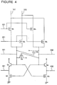
- FIG. 4 is a block diagram illustrating a fourth embodiment of the present invention.
- the circuit comprises bipolar transistors Q1 and Q2, PMOS transistors M5 and M6 and NMOS transistors M1, M2, M3, M4, M7 and M8. It also comprises input terminals 101, 102 and 201, 202 and output terminals 301, 302 and 401, 402.
- the input terminals 101 and 102 receive a pair of complementary signals A and A ⁇ having an inverted value to each other, respectively, and similarly, the input terminals 201 and 202 receive a pair of complementary signals B and B ⁇ , respectively.
- the signal B is "1"
- the NMOS transistors M1 and M3 are turned on and the transistors M2 and M4 are turned off.
- the values of the signals A and A ⁇ are outputted to the output terminals 301 and 302, respectively.
- the transistors M2 and M4 are turned on and the transistors M1 and M3 are turned off so that the values of the signals A ⁇ and A are outputted to the output terminal 302 and 301, respectively.
- an EX-NOR output and an EX-OR output are obtained at the output terminals 302 and 301, respectively.
- the EX-OR and EX-NOR output signals are obtained only by passing through the NMOS transistors so that this circuit can operate at a high speed.
- the high voltage level of the signal which has passed through the NMOS transistors is lower than the power supply voltage by a threshold voltage Vt of the MOS transistors.
- the signals at the output terminal 301 and 302 are amplified to the power supply voltage by the PMOS transistors M5 and M6.
- the signals inputted from the input terminals 201 and 202 control the gates of the MOS transistors. If the high level of these signal is low, the NMOS transistors controlled by the signal have a high channel resistance so that the signal propagation speed is low. Then, the signals of the output terminals 301 and 302 are supplied to the input terminals 201 and 202.
- the signals at the output terminals 301 and 302 are amplified by a BiNMOS type circuit in order to drive a large load.
- the output terminals 401 and 402 are used to drive the source of the transfer gate and the large capacitance load of the logic circuit of the following stage to be driven.
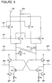
- FIG. 5 is a block diagram illustrating a fifth embodiment of the present invention.
- the circuit comprises bipolar transistors Q3, Q4, Q5 and Q6, PMOS transistors M5 and M6, NMOS transistors M1, M2, M3, M4, M9 and M10 and resistors R1 and R2. It also comprises input terminals 101, 102 and 201, 202 and output terminals 301, 302 and 501, 502.
- the input terminals 101 and 102 receives a pair of complementary signals A and A ⁇ having an inverted value to each other, respectively, and similarly, the input terminals 201 and 202 receive a pair of complementary signals B and B ⁇ , respectively.
- the EX-OR and EX-NOR output signals are obtained only by passing through the NMOS transistors so that this circuit can operate at a high speed.
- the high voltage level of the signal which has passed through the NMOS transistors is lower than the power supply voltage by a threshold voltage Vt of the MOS transistors.
- the signals at the output terminals 301 and 302 are amplified to the power supply voltage by the PMOS transistors M5 and M6.
- the signals inputted from the input terminals 201 and 202 control the gates of the MOS transistors. If the high level of these signal is low, the NMOS transistors controlled by the signals have a high channel resistance so that the signal propagation speed is low.
- the signals of the output terminals 301 and 302 are supplied to the input terminals 201 and 202. Further, the signals at the output terminals 301 and 302 are amplified by a BiCMOS type circuit in order to drive a large load.
- the output terminals 401 and 402 are used to drive the source of the transfer gate and the large capacitance load of the logic circuit of the following stage to be driven.
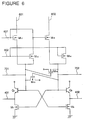
- FIG. 6 is a block diagram illustrating a sixth embodiment of the present invention.
- the circuit comprises bipolar transistors Q1 and Q2, PMOS transistors M15 and M16 and NMOS transistors M11, M12, M13, M14, M7 and M8. It also comprises input terminals 801, 802 and 601, 602 and output terminals 701, 702 and 401, 402.
- the input terminals 801 and 802 receive a pair of complementary signals A and A ⁇ having an inverted value to each other, respectively, and similarly, the input terminals 601 and 602 receive a pair of complementary signals B and B ⁇ , respectively.
- the signal B is "1"
- the NMOS transistors M11 and M12 are turned on and the transistors M13 and M14 are turned off.
- the values of the signals A and A ⁇ are outputted to the outputs terminal 701 and 702, respectively.
- the transistors M13 and M14 are turned on and the transistors M11 and M12 are turned off so that the values of the signals B and B ⁇ are outputted to the output terminals 701 and 702, respectively.
- an AND output and a NAND output are obtained at the output terminals 701 and 702, respectively.
- the AND and NAND output signals are obtained only by passing through the NMOS transistors so that this circuit can operate at a high speed.
- the high voltage level of the signal which has passed through the NMOS transistors is lower than the power supply voltage by a threshold voltage Vt of the MOS transistors.
- the drains of the PMOS transistors are connected to the output terminals 701 and 702 and the sources are connected to the power supply voltage terminal so that the high voltage level of the input signal is pulled up to the power supply voltage level.
- the signals inputted from the input terminals 601 and 602 control the gates of the MOS transistors. If the high level of these signals is low, the NMOS transistors controlled by the signals have a high channel resistance so that the signal propagation speed is low. Then, the signals of the output terminals 701 and 702 are supplied to the input terminals 601 and 602. Further, the signals at the output terminal 701 and 702 are amplified by a BiCMOS type circuit in order to drive a large load.
- the output terminals 401 and 402 are used to drive the source of the transfer gate and the large capacitance load of the logic circuit of the following stage to be driven.
- FIG. 7 is a block diagram illustrating a seventh embodiment of the present invention.
- the circuit comprises bipolar transistors Q3, Q4, Q5 and Q6, PMOS transistors M15 and M16, NMOS transistors M11, M12, M13, M14, M9 and M10 and resistors R1 and R2. It also comprises input terminals 801, 802 and 601, 602 and output terminals 701, 702 and 501, 502.
- the input terminals 801 and 802 receive a pair of complementary signals A and A ⁇ having an inverted value to each other, respectively, and similarly, the input terminals 601 and 602 receive a pair of complementary signals B and B ⁇ , respectively.
- the high voltage level of the signal which has passed through the NMOS transistors is lower than the power supply voltage by a threshold voltage Vt of the MOS transistors.
- the drains of the PMOS transistors are connected to the output terminals 701 and 702 and the sources are connected to the power supply voltage terminal so that the high voltage level of the input signal is pulled up to the power supply voltage level.
- the signals inputted from the input terminals 601 and 602 control the gates of the MOS transistors. If the high level of this signal is low, the NMOS transistor controlled by the signal has a high channel resistance so that the signal propagation speed is low. Then, the signals of the output terminals 701 and 702 are supplied to the input terminals 601 and 602.
- the signals at the output terminal 701 and 702 are amplified by a BiCMOS circuit in order to drive a large load.
- the output terminals 401 and 402 are used to drive the source of the transfer gate and the large capacitance load of the logic circuit of the following stage to be driven.
- CMOS level and the BiNMOS level are used. These levels are used properly and propagated to the logic circuit of the following stage so that the high-speed operation can be realized.
- two output signal levels of the pass logic EX-OR and EXNOR circuits that is, die CMOS level and the BiCMOS level are used. These levels are used properly and propagated to the logic circuit of tee following stage so that the high-speed operation can be realized.
- two output signal levels of the pass logic AND, NAND, OR and NOR circuits that is, the CMOS level and the BiNMOS level are used. These levels are used, properly and propagated to the logic circuit of the following stage so that the high-speed operation can be realized.
- CMOS level and the BiCMOS level are used. These levels are used properly and propagated to the logic circuit of the following stage so that the high-speed operation can be realized.
Applications Claiming Priority (4)
| Application Number | Priority Date | Filing Date | Title |
|---|---|---|---|
| JP7023/92 | 1992-01-20 | ||
| JP4007023A JP2760195B2 (ja) | 1992-01-20 | 1992-01-20 | 論理回路 |
| JP39836/92 | 1992-02-26 | ||
| JP4039836A JP2903835B2 (ja) | 1992-02-26 | 1992-02-26 | 論理回路 |
Publications (2)
| Publication Number | Publication Date |
|---|---|
| EP0552734A2 true EP0552734A2 (fr) | 1993-07-28 |
| EP0552734A3 EP0552734A3 (en) | 1993-10-27 |
Family
ID=26341255
Family Applications (1)
| Application Number | Title | Priority Date | Filing Date |
|---|---|---|---|
| EP19930100798 Withdrawn EP0552734A3 (en) | 1992-01-20 | 1993-01-20 | High speed logic circuit having a reduced number of critical path gate stages |
Country Status (1)
| Country | Link |
|---|---|
| EP (1) | EP0552734A3 (fr) |
Cited By (2)
| Publication number | Priority date | Publication date | Assignee | Title |
|---|---|---|---|---|
| US5898322A (en) * | 1994-09-13 | 1999-04-27 | Sharp Kabushiki Kaisha | Logic circuit for liquid crystal display having pass-transistor logic circuitry and thin film transistors |
| DE102005008367B3 (de) * | 2005-02-23 | 2006-10-19 | Infineon Technologies Ag | XOR-Schaltung |
Citations (2)
| Publication number | Priority date | Publication date | Assignee | Title |
|---|---|---|---|---|
| JPS58165424A (ja) * | 1982-03-26 | 1983-09-30 | Nec Corp | 排他論理和回路 |
| EP0435389A2 (fr) * | 1989-12-28 | 1991-07-03 | Koninklijke Philips Electronics N.V. | Multiplexeurs et portes logiques BICMOS à entrées et sorties différentielles et un additionneur utilisant ceux-ci |
-
1993
- 1993-01-20 EP EP19930100798 patent/EP0552734A3/en not_active Withdrawn
Patent Citations (2)
| Publication number | Priority date | Publication date | Assignee | Title |
|---|---|---|---|---|
| JPS58165424A (ja) * | 1982-03-26 | 1983-09-30 | Nec Corp | 排他論理和回路 |
| EP0435389A2 (fr) * | 1989-12-28 | 1991-07-03 | Koninklijke Philips Electronics N.V. | Multiplexeurs et portes logiques BICMOS à entrées et sorties différentielles et un additionneur utilisant ceux-ci |
Non-Patent Citations (3)
| Title |
|---|
| IBM TECHNICAL DISCLOSURE BULLETIN vol. 32, no. 8B, January 1990, pages 94 - 95 ANON 'DENSE CMOS EX-OR AND EX-NOR CIRCUITS' * |
| PATENT ABSTRACTS OF JAPAN vol. 7, no. 288 (E-218)(1433) 22 December 1983 & JP-A-58 165 424 ( NIPPON DENKI K.K. ) 30 September 1983 * |
| PROCEEDINGS OF THE 32ND MIDWEST SYMPOSIUM ON CIRCUITS AND SYSTEMS August 1989, CHAMPAIGN, IL., US pages 829 - 832 D. HUANG ET AL. 'On CMOS Exclusive OR Design' * |
Cited By (3)
| Publication number | Priority date | Publication date | Assignee | Title |
|---|---|---|---|---|
| US5898322A (en) * | 1994-09-13 | 1999-04-27 | Sharp Kabushiki Kaisha | Logic circuit for liquid crystal display having pass-transistor logic circuitry and thin film transistors |
| DE102005008367B3 (de) * | 2005-02-23 | 2006-10-19 | Infineon Technologies Ag | XOR-Schaltung |
| US7358769B2 (en) | 2005-02-23 | 2008-04-15 | Infineon Technologies Ag | XOR circuit |
Also Published As
| Publication number | Publication date |
|---|---|
| EP0552734A3 (en) | 1993-10-27 |
Similar Documents
| Publication | Publication Date | Title |
|---|---|---|
| US4710649A (en) | Transmission-gate structured logic circuits | |
| US4883988A (en) | Current mirror switching circuit | |
| JP2760195B2 (ja) | 論理回路 | |
| US5604417A (en) | Semiconductor integrated circuit device | |
| US4725982A (en) | Tri-state buffer circuit | |
| US5155387A (en) | Circuit suitable for differential multiplexers and logic gates utilizing bipolar and field-effect transistors | |
| US5548231A (en) | Serial differential pass gate logic design | |
| US4395645A (en) | Mosfet logic inverter buffer circuit for integrated circuits | |
| US5280204A (en) | ECI compatible CMOS off-chip driver using feedback to set output levels | |
| KR100211791B1 (ko) | Ic칩과 이를 위한 패스 게이트 논리군 | |
| EP0552734A2 (fr) | Circuit logique à haute vitesse de commutation avec un nombre réduit des portes dans le chemin critique | |
| US7138834B2 (en) | Symmetric differential logic circuits | |
| EP0196616A2 (fr) | Circuit logique | |
| US5936427A (en) | Three-input exclusive NOR circuit | |
| US5495182A (en) | Fast-fully restoring polarity control circuit | |
| EP0435389B1 (fr) | Multiplexeurs et portes logiques BICMOS à entrées et sorties différentielles et un additionneur utilisant ceux-ci | |
| JP2551586B2 (ja) | インタフエ−ス回路 | |
| JPH07183793A (ja) | レベル変換回路 | |
| JPS59123930A (ja) | 桁上げ信号発生器 | |
| KR100410813B1 (ko) | 반도체소자의고속저전력구동회로를구현하기위한인버터 | |
| JP3697872B2 (ja) | 論理回路 | |
| GB2306816A (en) | CMOS exclusive OR circuit | |
| KR100500922B1 (ko) | 저전압에서 안정적인 연산 동작을 수행하기위한 논리 연산 회로 | |
| JP2867253B2 (ja) | 3入力エクスクルシーブオアゲート | |
| KR100278992B1 (ko) | 전가산기 |
Legal Events
| Date | Code | Title | Description |
|---|---|---|---|
| PUAI | Public reference made under article 153(3) epc to a published international application that has entered the european phase |
Free format text: ORIGINAL CODE: 0009012 |
|
| AK | Designated contracting states |
Kind code of ref document: A2 Designated state(s): DE FR GB |
|
| PUAL | Search report despatched |
Free format text: ORIGINAL CODE: 0009013 |
|
| AK | Designated contracting states |
Kind code of ref document: A3 Designated state(s): DE FR GB |
|
| 17P | Request for examination filed |
Effective date: 19930914 |
|
| STAA | Information on the status of an ep patent application or granted ep patent |
Free format text: STATUS: THE APPLICATION HAS BEEN WITHDRAWN |
|
| 18W | Application withdrawn |
Withdrawal date: 19940927 |