EP0549994B1 - Global planarization process - Google Patents
Global planarization process Download PDFInfo
- Publication number
- EP0549994B1 EP0549994B1 EP92121777A EP92121777A EP0549994B1 EP 0549994 B1 EP0549994 B1 EP 0549994B1 EP 92121777 A EP92121777 A EP 92121777A EP 92121777 A EP92121777 A EP 92121777A EP 0549994 B1 EP0549994 B1 EP 0549994B1
- Authority
- EP
- European Patent Office
- Prior art keywords
- layer
- recited
- planarization
- tin
- planarization layer
- Prior art date
- Legal status (The legal status is an assumption and is not a legal conclusion. Google has not performed a legal analysis and makes no representation as to the accuracy of the status listed.)
- Expired - Lifetime
Links
Images
Classifications
-
- H10P76/2041—
-
- H—ELECTRICITY
- H01—ELECTRIC ELEMENTS
- H01L—SEMICONDUCTOR DEVICES NOT COVERED BY CLASS H10
- H01L21/00—Processes or apparatus adapted for the manufacture or treatment of semiconductor or solid state devices or of parts thereof
- H01L21/02—Manufacture or treatment of semiconductor devices or of parts thereof
- H01L21/027—Making masks on semiconductor bodies for further photolithographic processing not provided for in group H01L21/18 or H01L21/34
- H01L21/0271—Making masks on semiconductor bodies for further photolithographic processing not provided for in group H01L21/18 or H01L21/34 comprising organic layers
- H01L21/0273—Making masks on semiconductor bodies for further photolithographic processing not provided for in group H01L21/18 or H01L21/34 comprising organic layers characterised by the treatment of photoresist layers
- H01L21/0274—Photolithographic processes
-
- H—ELECTRICITY
- H01—ELECTRIC ELEMENTS
- H01L—SEMICONDUCTOR DEVICES NOT COVERED BY CLASS H10
- H01L21/00—Processes or apparatus adapted for the manufacture or treatment of semiconductor or solid state devices or of parts thereof
- H01L21/02—Manufacture or treatment of semiconductor devices or of parts thereof
- H01L21/04—Manufacture or treatment of semiconductor devices or of parts thereof the devices having potential barriers, e.g. a PN junction, depletion layer or carrier concentration layer
- H01L21/18—Manufacture or treatment of semiconductor devices or of parts thereof the devices having potential barriers, e.g. a PN junction, depletion layer or carrier concentration layer the devices having semiconductor bodies comprising elements of Group IV of the Periodic Table or AIIIBV compounds with or without impurities, e.g. doping materials
- H01L21/30—Treatment of semiconductor bodies using processes or apparatus not provided for in groups H01L21/20 - H01L21/26
- H01L21/31—Treatment of semiconductor bodies using processes or apparatus not provided for in groups H01L21/20 - H01L21/26 to form insulating layers thereon, e.g. for masking or by using photolithographic techniques; After treatment of these layers; Selection of materials for these layers
- H01L21/3105—After-treatment
- H01L21/31051—Planarisation of the insulating layers
-
- H—ELECTRICITY
- H01—ELECTRIC ELEMENTS
- H01L—SEMICONDUCTOR DEVICES NOT COVERED BY CLASS H10
- H01L21/00—Processes or apparatus adapted for the manufacture or treatment of semiconductor or solid state devices or of parts thereof
- H01L21/02—Manufacture or treatment of semiconductor devices or of parts thereof
- H01L21/04—Manufacture or treatment of semiconductor devices or of parts thereof the devices having potential barriers, e.g. a PN junction, depletion layer or carrier concentration layer
- H01L21/18—Manufacture or treatment of semiconductor devices or of parts thereof the devices having potential barriers, e.g. a PN junction, depletion layer or carrier concentration layer the devices having semiconductor bodies comprising elements of Group IV of the Periodic Table or AIIIBV compounds with or without impurities, e.g. doping materials
- H01L21/30—Treatment of semiconductor bodies using processes or apparatus not provided for in groups H01L21/20 - H01L21/26
- H01L21/31—Treatment of semiconductor bodies using processes or apparatus not provided for in groups H01L21/20 - H01L21/26 to form insulating layers thereon, e.g. for masking or by using photolithographic techniques; After treatment of these layers; Selection of materials for these layers
- H01L21/3205—Deposition of non-insulating-, e.g. conductive- or resistive-, layers on insulating layers; After-treatment of these layers
- H01L21/321—After treatment
- H01L21/32115—Planarisation
- H01L21/3212—Planarisation by chemical mechanical polishing [CMP]
-
- H10P52/403—
-
- H10P95/06—
Definitions
- the invention relates to a method of planarizing a structure on a substrate.
- CMP is the main and until now, the only proven global planarization technique which is being seriously considered for sub-0.5 ⁇ m technologies.
- successful implementations of CMP for semiconductor device manufacturing demands effective post-CMP cleaning process in order to remove the CMP-induced surface contaminants and damage. Much work remains to be done in order to make CMP a fully manufacturable and optimized process.
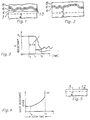
- Figure 1 is a cross-sectional drawing similar to figure 1, illustrating the etch-back end-point level before melting and resolidification but after deposition.
- Figure 2 is a cross-sectional drawing illustrating the resulting planarized structure up to the sixth processing step (after melting and resolidification).
- Figure 3 illustrates a graph of the surface reflectance R versus time t used for planarization process end-point detection.
- Figure 4 illustrates a graph showing sheet resistance measured in ohms per square versus etch time t which is also useful for planarization process end-point detection.
- Figure 5 is a cross-sectional which illustrates the resulting structure after the etch-back step indicating a globally planarized surface.
- the invention provides a process which is simple to implement, for global planarization of semiconductor chips.
- This process provides true global planarization (e.g. on the lateral scale of 1000's of ⁇ m to several centimeters) and can be used instead of CMP.
- the invention's global planarization process does not employ any mechanical polishing and, as a result, does not require any post-planarization surface cleaning such as the special post-CMP cleaning requirements.
- This invention is fully compatible with existing semiconductor processing equipment.
- this invention is fully compatible with various metallization systems (e.g. Al/SiO 2 , Cu/SiO 2 , W/SiO 2 , Au/SiO 2 and etc.) and can be employed before and/or after each metal level in multi-level metal technologies.
- the disclosed process can be appropriately called metal-melt solidification planarization (MMSP).
- MMSP metal-melt solidification planarization
- This global planarization process can be used to form planarized dielectric, metal, or semiconductor surfaces.
- the process flow to be described here is for dielectric planarization.
- a suggested process flow based on the global planarization of this invention is as follows (assuming a 3-level metal semiconductor technology, although note that technologies with fewer or more levels of metal can suitably be adapted for use with the following process): 1) Complete the device fabrication process flow on a semiconductor wafer through all the steps for fabrication of the active devices. In other words complete the fabrication flow up to a point just prior to the first metal level. 2) Deposit the first interlevel dielectric (ILD) 3 such as PSG or BPSG or undoped oxide (or a stacked combination thereof).
- ILD interlevel dielectric
- a diffused barrier layer 4 such as plasma deposited silicon nitride.
- This layer is optional depending upon the type of disposable planarization layer used as will be explained further.
- the barrier layer will act as a diffusion barrier and is disposable. The barrier layer prevents diffusion of the disposable planarization layer atoms into the substrate on which the active devices lie.
- Suitable material for the buffer/adhesion layer includes materials such as polysilicon, titanium, aluminum or their alloys. This can be done using physical-vapor deposition (PVD) such as sputtering or this can be done using chemical-vapor deposition(CVD). Other adhesion or glue layer mateials may be used. 5) Deposit a relatively thick layer (e.g. a layer 1 ⁇ m to a few microns thick) of a low melting point (a low melting point being considered below 400°C) and high boiling point (a high boiling point being considered above 1500°C) elemental metal or suitable alloy. This relatively thick layer shall serve as a disposable planarization layer.
- Tin, indium and bismuth are considered suitable materials as shown below in table A which indicates melting point and boiling point temperatures at atmospheric pressure in Celsius.
- Tin is considered the metal of preferred choice since it meets the melting and boiling point requirements for the planarization layer at melting point temperatures that are not deleterious to conventional metal layers such as aluminum. Restated, the requirements for the planarization layer are that it should melt without evaporating at relatively low temperatures and, therefore, that it have a low vapor pressure at temperatures below 1000°C. Tin is also fairly cheap and abundant. Indium is much more expensive than tin. Bismuth forms low melting point alloys with tin. Bismuth is also fairly cheap.
- tin, indium, bismuth or their alloys can be used for the application of this invention due to their low melting points (below 300°C), high boiling points, and very low vapor pressures below 1000°C. In fact, their vapor pressures are extremely low at less than 500°C.
- the deposition process for the planarization layer can be accomplished by a physical-vapor deposition process (PVD) such as sputtering or it can be accomplished by chemical-vapor deposition (CVD) if a CVD precursor is available.
- PVD physical-vapor deposition
- CVD chemical-vapor deposition
- tin tin tetrachlorie
- SnH 4 tin hydride
- the thickness of a sputtered or evaporated (or CVD-formed) tin planarization layer is selected such that sufficient tin material layer is available to cover the entire nonplanar topography when molten planar tin metal is formed later on.
- the tin layer thicknesses of 1-4 ⁇ m are sufficiently large to achieve global planarization over semiconductor integrated circuits.
- the barrier layer is not always needed. This is likely the case when tin is used as the disposable planarization layer. Tin is a column IV metal in the periodic table as is silicon the likely semiconductor substrate. Therefore, tin does not act as a generation/recombination (defect) center with respect to a silicon semiconductor substrate. Consequently, the barrier layer can probably be omitted with this planarization layer/substrate combination.
- Figure 1 is a cross-sectional drawing illustrating the resulting structure from the foregoing processing steps. Shown in figure 1 are substrate 2, interlevel dielectric layer 3, adhesion layer 6, barrier layer 4 and planarization layer 8.
- planarization steps tin sputter deposition or tin CVD, wafer heating/tin melting, wafer cooling/ tin solidification, tin etch-back
- tin sputter deposition or tin CVD wafer heating/tin melting
- wafer cooling/ tin solidification wafer cooling/ tin solidification
- tin etch-back the entire sequence of planarization steps can be performed in-situ within a single PVD or CVD chamber.
- the deposition process of the planarization layer can be performed while the wafer is heated to above the melting point of tin (e.g. between 232°C and 400°C). This will result in formation of globally planar tin melt during the deposition. As a result, the two steps of tin deposition and melt resolidification can be performed in a single process step.
- tin melting point
Landscapes
- Engineering & Computer Science (AREA)
- Physics & Mathematics (AREA)
- Condensed Matter Physics & Semiconductors (AREA)
- General Physics & Mathematics (AREA)
- Manufacturing & Machinery (AREA)
- Computer Hardware Design (AREA)
- Microelectronics & Electronic Packaging (AREA)
- Power Engineering (AREA)
- Internal Circuitry In Semiconductor Integrated Circuit Devices (AREA)
- Drying Of Semiconductors (AREA)
- Formation Of Insulating Films (AREA)
Applications Claiming Priority (2)
| Application Number | Priority Date | Filing Date | Title |
|---|---|---|---|
| US816458 | 1991-12-31 | ||
| US07/816,458 US5284804A (en) | 1991-12-31 | 1991-12-31 | Global planarization process |
Publications (3)
| Publication Number | Publication Date |
|---|---|
| EP0549994A2 EP0549994A2 (en) | 1993-07-07 |
| EP0549994A3 EP0549994A3 (en) | 1993-07-28 |
| EP0549994B1 true EP0549994B1 (en) | 1996-07-17 |
Family
ID=25220681
Family Applications (1)
| Application Number | Title | Priority Date | Filing Date |
|---|---|---|---|
| EP92121777A Expired - Lifetime EP0549994B1 (en) | 1991-12-31 | 1992-12-22 | Global planarization process |
Country Status (5)
| Country | Link |
|---|---|
| US (1) | US5284804A (show.php) |
| EP (1) | EP0549994B1 (show.php) |
| JP (1) | JP3361847B2 (show.php) |
| DE (1) | DE69212295T2 (show.php) |
| TW (1) | TW256934B (show.php) |
Families Citing this family (18)
| Publication number | Priority date | Publication date | Assignee | Title |
|---|---|---|---|---|
| US5354695A (en) * | 1992-04-08 | 1994-10-11 | Leedy Glenn J | Membrane dielectric isolation IC fabrication |
| US6714625B1 (en) * | 1992-04-08 | 2004-03-30 | Elm Technology Corporation | Lithography device for semiconductor circuit pattern generation |
| US6355553B1 (en) * | 1992-07-21 | 2002-03-12 | Sony Corporation | Method of forming a metal plug in a contact hole |
| US6690044B1 (en) | 1993-03-19 | 2004-02-10 | Micron Technology, Inc. | Approach to avoid buckling BPSG by using an intermediate barrier layer |
| US5372974A (en) * | 1993-03-19 | 1994-12-13 | Micron Semiconductor, Inc. | Approach to avoid buckling in BPSG by using an intermediate barrier layer |
| US5532188A (en) * | 1994-03-30 | 1996-07-02 | Wright; Peter J. | Global planarization of multiple layers |
| KR0159388B1 (ko) * | 1995-09-30 | 1999-02-01 | 배순훈 | 평탄화 방법 |
| US5885900A (en) * | 1995-11-07 | 1999-03-23 | Lucent Technologies Inc. | Method of global planarization in fabricating integrated circuit devices |
| US5837603A (en) * | 1996-05-08 | 1998-11-17 | Harris Corporation | Planarization method by use of particle dispersion and subsequent thermal flow |
| US6551857B2 (en) * | 1997-04-04 | 2003-04-22 | Elm Technology Corporation | Three dimensional structure integrated circuits |
| US5915167A (en) * | 1997-04-04 | 1999-06-22 | Elm Technology Corporation | Three dimensional structure memory |
| JP2001516970A (ja) * | 1997-09-18 | 2001-10-02 | シーブイシー プロダクツ、インコーポレイテッド | 高性能集積回路の相互接続製造の方法及び装置 |
| US6335288B1 (en) * | 2000-08-24 | 2002-01-01 | Applied Materials, Inc. | Gas chemistry cycling to achieve high aspect ratio gapfill with HDP-CVD |
| US7402897B2 (en) * | 2002-08-08 | 2008-07-22 | Elm Technology Corporation | Vertical system integration |
| KR100587635B1 (ko) * | 2003-06-10 | 2006-06-07 | 주식회사 하이닉스반도체 | 반도체소자의 제조 방법 |
| US20090074962A1 (en) * | 2007-09-14 | 2009-03-19 | Asml Netherlands B.V. | Method for the protection of an optical element of a lithographic apparatus and device manufacturing method |
| JP2014053502A (ja) * | 2012-09-07 | 2014-03-20 | Toshiba Corp | 半導体装置の製造方法 |
| JP2023002853A (ja) * | 2019-12-12 | 2023-01-11 | Agc株式会社 | 積層基板、及びその製造方法 |
Family Cites Families (14)
| Publication number | Priority date | Publication date | Assignee | Title |
|---|---|---|---|---|
| US4655874A (en) * | 1985-07-26 | 1987-04-07 | Advanced Micro Devices, Inc. | Process for smoothing a non-planar surface |
| US4676868A (en) * | 1986-04-23 | 1987-06-30 | Fairchild Semiconductor Corporation | Method for planarizing semiconductor substrates |
| US4775550A (en) * | 1986-06-03 | 1988-10-04 | Intel Corporation | Surface planarization method for VLSI technology |
| US4708770A (en) * | 1986-06-19 | 1987-11-24 | Lsi Logic Corporation | Planarized process for forming vias in silicon wafers |
| US4732658A (en) * | 1986-12-03 | 1988-03-22 | Honeywell Inc. | Planarization of silicon semiconductor devices |
| US4810335A (en) * | 1987-01-20 | 1989-03-07 | Siemens Aktiengesellschaft | Method for monitoring etching processes |
| US4983545A (en) * | 1987-03-20 | 1991-01-08 | Nec Corporation | Planarization of dielectric films on integrated circuits |
| US4839311A (en) * | 1987-08-14 | 1989-06-13 | National Semiconductor Corporation | Etch back detection |
| JPH063804B2 (ja) * | 1988-01-21 | 1994-01-12 | シャープ株式会社 | 半導体装置製造方法 |
| KR920000708B1 (ko) * | 1988-07-22 | 1992-01-20 | 현대전자산업 주식회사 | 포토레지스트 에치백 기술을 이용한 트렌치 캐패시터 형성방법 |
| US4962063A (en) * | 1988-11-10 | 1990-10-09 | Applied Materials, Inc. | Multistep planarized chemical vapor deposition process with the use of low melting inorganic material for flowing while depositing |
| US5183781A (en) * | 1990-01-12 | 1993-02-02 | Nec Corporation | Method of manufacturing semiconductor device |
| JP2518435B2 (ja) * | 1990-01-29 | 1996-07-24 | ヤマハ株式会社 | 多層配線形成法 |
| US5143867A (en) * | 1991-02-13 | 1992-09-01 | International Business Machines Corporation | Method for depositing interconnection metallurgy using low temperature alloy processes |
-
1991
- 1991-12-31 US US07/816,458 patent/US5284804A/en not_active Expired - Lifetime
-
1992
- 1992-12-22 DE DE69212295T patent/DE69212295T2/de not_active Expired - Fee Related
- 1992-12-22 EP EP92121777A patent/EP0549994B1/en not_active Expired - Lifetime
-
1993
- 1993-01-04 JP JP02957193A patent/JP3361847B2/ja not_active Expired - Fee Related
- 1993-04-21 TW TW082103037A patent/TW256934B/zh not_active IP Right Cessation
Non-Patent Citations (1)
| Title |
|---|
| JOURNAL OF THE ELECTROCHEMICAL SOCIETY: SOLID-STATE SCIENCE AND TECHNOLOGY, vol. 128, no. 2, February 1981, pages 423-429 * |
Also Published As
| Publication number | Publication date |
|---|---|
| EP0549994A3 (en) | 1993-07-28 |
| TW256934B (show.php) | 1995-09-11 |
| JP3361847B2 (ja) | 2003-01-07 |
| US5284804A (en) | 1994-02-08 |
| DE69212295D1 (de) | 1996-08-22 |
| EP0549994A2 (en) | 1993-07-07 |
| JPH06120180A (ja) | 1994-04-28 |
| DE69212295T2 (de) | 1997-02-06 |
Similar Documents
| Publication | Publication Date | Title |
|---|---|---|
| EP0549994B1 (en) | Global planarization process | |
| KR0177537B1 (ko) | 표면 확산에 의한 높은 종횡비 및 낮은 비저항의 라인/비어 | |
| US5578523A (en) | Method for forming inlaid interconnects in a semiconductor device | |
| US6461675B2 (en) | Method for forming a copper film on a substrate | |
| US6489230B1 (en) | Integration of low-k SiOF as inter-layer dielectric | |
| EP0721216B1 (en) | A soft metal conductor and method of making | |
| US5994217A (en) | Post metallization stress relief annealing heat treatment for ARC TiN over aluminum layers | |
| US6255217B1 (en) | Plasma treatment to enhance inorganic dielectric adhesion to copper | |
| US6309970B1 (en) | Method of forming multi-level copper interconnect with formation of copper oxide on exposed copper surface | |
| EP1313140A1 (en) | Method of forming a liner for tungsten plugs | |
| US6548415B2 (en) | Method for the etchback of a conductive material | |
| US5783493A (en) | Method for reducing precipitate defects using a plasma treatment post BPSG etchback | |
| US6713407B1 (en) | Method of forming a metal nitride layer over exposed copper | |
| KR100308467B1 (ko) | 기판내의서브마이크론비아충전방법 | |
| US6887353B1 (en) | Tailored barrier layer which provides improved copper interconnect electromigration resistance | |
| US6468908B1 (en) | Al-Cu alloy sputtering method with post-metal quench | |
| US6734101B1 (en) | Solution to the problem of copper hillocks | |
| US5904558A (en) | Fabrication process of semiconductor device | |
| US6867142B2 (en) | Method to prevent electrical shorts between tungsten interconnects | |
| US6200894B1 (en) | Method for enhancing aluminum interconnect properties | |
| JPH0922907A (ja) | 埋め込み導電層の形成方法 | |
| US6017816A (en) | Method of fabricating A1N anti-reflection coating on metal layer | |
| US6576551B1 (en) | Chemical mechanical polish planarizing method with pressure compensating layer | |
| US5936307A (en) | Surface modification method for film stress reduction | |
| US20250054809A1 (en) | Fully self-aligned via with graphene cap |
Legal Events
| Date | Code | Title | Description |
|---|---|---|---|
| PUAI | Public reference made under article 153(3) epc to a published international application that has entered the european phase |
Free format text: ORIGINAL CODE: 0009012 |
|
| PUAL | Search report despatched |
Free format text: ORIGINAL CODE: 0009013 |
|
| AK | Designated contracting states |
Kind code of ref document: A2 Designated state(s): DE FR GB IT NL |
|
| AK | Designated contracting states |
Kind code of ref document: A3 Designated state(s): DE FR GB IT NL |
|
| 17P | Request for examination filed |
Effective date: 19931207 |
|
| 17Q | First examination report despatched |
Effective date: 19941004 |
|
| GRAH | Despatch of communication of intention to grant a patent |
Free format text: ORIGINAL CODE: EPIDOS IGRA |
|
| GRAH | Despatch of communication of intention to grant a patent |
Free format text: ORIGINAL CODE: EPIDOS IGRA |
|
| GRAA | (expected) grant |
Free format text: ORIGINAL CODE: 0009210 |
|
| ITF | It: translation for a ep patent filed | ||
| AK | Designated contracting states |
Kind code of ref document: B1 Designated state(s): DE FR GB IT NL |
|
| PG25 | Lapsed in a contracting state [announced via postgrant information from national office to epo] |
Ref country code: NL Free format text: LAPSE BECAUSE OF FAILURE TO SUBMIT A TRANSLATION OF THE DESCRIPTION OR TO PAY THE FEE WITHIN THE PRESCRIBED TIME-LIMIT Effective date: 19960717 |
|
| REF | Corresponds to: |
Ref document number: 69212295 Country of ref document: DE Date of ref document: 19960822 |
|
| ET | Fr: translation filed | ||
| NLV1 | Nl: lapsed or annulled due to failure to fulfill the requirements of art. 29p and 29m of the patents act | ||
| PLBE | No opposition filed within time limit |
Free format text: ORIGINAL CODE: 0009261 |
|
| STAA | Information on the status of an ep patent application or granted ep patent |
Free format text: STATUS: NO OPPOSITION FILED WITHIN TIME LIMIT |
|
| 26N | No opposition filed | ||
| REG | Reference to a national code |
Ref country code: GB Ref legal event code: IF02 |
|
| PGFP | Annual fee paid to national office [announced via postgrant information from national office to epo] |
Ref country code: IT Payment date: 20061231 Year of fee payment: 15 |
|
| PGFP | Annual fee paid to national office [announced via postgrant information from national office to epo] |
Ref country code: GB Payment date: 20071106 Year of fee payment: 16 |
|
| PGFP | Annual fee paid to national office [announced via postgrant information from national office to epo] |
Ref country code: DE Payment date: 20071228 Year of fee payment: 16 |
|
| PGFP | Annual fee paid to national office [announced via postgrant information from national office to epo] |
Ref country code: FR Payment date: 20071204 Year of fee payment: 16 |
|
| GBPC | Gb: european patent ceased through non-payment of renewal fee |
Effective date: 20081222 |
|
| PG25 | Lapsed in a contracting state [announced via postgrant information from national office to epo] |
Ref country code: IT Free format text: LAPSE BECAUSE OF NON-PAYMENT OF DUE FEES Effective date: 20071222 |
|
| REG | Reference to a national code |
Ref country code: FR Ref legal event code: ST Effective date: 20090831 |
|
| PG25 | Lapsed in a contracting state [announced via postgrant information from national office to epo] |
Ref country code: DE Free format text: LAPSE BECAUSE OF NON-PAYMENT OF DUE FEES Effective date: 20090701 |
|
| PG25 | Lapsed in a contracting state [announced via postgrant information from national office to epo] |
Ref country code: GB Free format text: LAPSE BECAUSE OF NON-PAYMENT OF DUE FEES Effective date: 20081222 |
|
| PG25 | Lapsed in a contracting state [announced via postgrant information from national office to epo] |
Ref country code: FR Free format text: LAPSE BECAUSE OF NON-PAYMENT OF DUE FEES Effective date: 20081231 |