EP0540276B1 - Herstellungsverfahren eines selbstjustierenden Kontakts - Google Patents
Herstellungsverfahren eines selbstjustierenden Kontakts Download PDFInfo
- Publication number
- EP0540276B1 EP0540276B1 EP92309796A EP92309796A EP0540276B1 EP 0540276 B1 EP0540276 B1 EP 0540276B1 EP 92309796 A EP92309796 A EP 92309796A EP 92309796 A EP92309796 A EP 92309796A EP 0540276 B1 EP0540276 B1 EP 0540276B1
- Authority
- EP
- European Patent Office
- Prior art keywords
- barrier layer
- insulating layer
- gate electrode
- layer
- sidewall spacers
- Prior art date
- Legal status (The legal status is an assumption and is not a legal conclusion. Google has not performed a legal analysis and makes no representation as to the accuracy of the status listed.)
- Expired - Lifetime
Links
Images
Classifications
-
- H—ELECTRICITY
- H01—ELECTRIC ELEMENTS
- H01L—SEMICONDUCTOR DEVICES NOT COVERED BY CLASS H10
- H01L21/00—Processes or apparatus adapted for the manufacture or treatment of semiconductor or solid state devices or of parts thereof
- H01L21/70—Manufacture or treatment of devices consisting of a plurality of solid state components formed in or on a common substrate or of parts thereof; Manufacture of integrated circuit devices or of parts thereof
- H01L21/71—Manufacture of specific parts of devices defined in group H01L21/70
- H01L21/768—Applying interconnections to be used for carrying current between separate components within a device comprising conductors and dielectrics
- H01L21/76897—Formation of self-aligned vias or contact plugs, i.e. involving a lithographically uncritical step
Definitions
- the present invention relates generally to semiconductor integrated circuits, and more specifically to the formation of self-aligned contacts in an integrated circuit.
- the self-aligned contact is widely used in high density circuits in order to save area.
- One approach to forming a self-aligned contact is to use a thick layer of oxide on top of a conductive layer in a gate. The purpose of the thick oxide layer is to protect the conductive layer during subsequent processing steps.
- anisotropic etches are performed when fabricating gates and vias in an integrated circuit. It is common to overetch a layer to ensure complete removal of the material.
- the thick oxide protects the conductive layer from being etched into during formation of the gates and vias. This prevents the conductive layer from connecting to an active area in the substrate, which would result in shorting out the component.
- the thick oxide required in this process increases the severity of the topography of the device. As one skilled in the art will recognize, the severe topography makes subsequent processing steps more difficult. Tall features result in step coverage problems for later interconnect layers.
- EP-A-0315229 discloses a method for forming a self-aligned contact comprising forming a gate electrode having a first insulatina laver and a barrier layer on the upper surface thereof, forming sidewall spacers alongside the gate electrode, wherein the barrier layer protects the gate electrode during formation of the sidewall spacers, depositing a second insulating layer over the device and opening a via through the second insulating layer.
- EP-A-0236123 discloses the use of metal nitride in the formation of a gate structure.
- a structure for an integrated circuit comprising a semiconductor substrate; a gate electrode; a first insulating layer having an upper surface, and disposed on the upper surface of the gate electrode; a barrier layer having an upper surface, and disposed on the upper surface of the first insulating layer; sidewall spacers alongside the vertical sidewalls of the gate electrode; and a second insulating layer positioned over a portion of the gate electrode characterised in that the barrier layer has a metallic conductor portion and a metal oxide insulator portion; the second insulating layer overlies a first part of the barrier layer; and the metal oxide insulator portion of the barrier layer forms the upper surface of the remainder of the barrier layer.
- a structure for an integrated circuit comprising a semiconductor substrate, a gate electrode, a first insulating layer having an upper surface, and disposed on the upper surface of the gate electrode; a barrier layer having an upper surface, disposed on the upper surface of the first insulating layer and covering less than the entirety of the upper surface of the first insulating layer; sidewall spacers alongside the vertical sidewalls of the gate electrode; and a second insulating layer positioned over a portion of the gate electrode characterised in that the barrier layer has a metallic conductor portion and a metal oxide insulator portion; the second insulating layer overlies the barrier layer; and an end portion of the barrier layer aligned with a side of the second insulating layer is formed from the metal oxide insulator portion, with the remainder of the barrier layer formed from the metallic conductor portion.
- a method for forming a self-aligned contact comprising the steps of forming a gate electrode having a first insulating layer and a barrier layer of a metallic conductive material on the upper surface thereof; forming sidewall spacers alongside the gate electrode, wherein the barrier layer protects the gate electrode during formation of the sidewall spacers; depositing a second insulating layer over the device; and opening a via through the second insulating layer, characterised by said opening step exposing a surface portion of the barrier layer and by thereafter converting said surface portion of the barrier layer into an insulating layer whereby said barrier layer comprises a metal oxide insulator portion and a metalic conductor portion.
- a method for forming a self-aligned contact comprising the steps of forming a gate electrode having a first insulating layer and a barrier layer of a metallic conductive material on the upper surface thereof; forming sidewall spacers alongside the gate electrode, wherein the barrier layer protects the gate electrode during formation of the sidewall spacers; depositing a second insulating layer over the device; and opening a via through the second insulating layer, characterised in that a portion of the remaining barrier layer is converted into an insulating area after formation of the via by oxidizing a portion of the barrier layer.
- a method for forming a self-aligned contact utilizes a thin insulating layer formed on the upper surface of a conductive layer.
- a barrier layer is deposited over the insulating layer, and gate electrodes are then defined. Sidewall spacers are formed along the vertical sidewalls of the gate electrodes. During formation of the sidewall spacers the barrier layer protects the gate electrodes.
- a second insulating layer is then deposited and a via is opened to the substrate. A contact can now be created by depositing conductive material into the via.
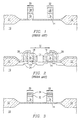
- Figures 1 and 2 depict a prior art process used to form a self-aligned contact.
- a self-aligned contact will be fabricated on a substrate 10 .
- Isolation regions of field oxide 12 are formed in and on the substrate 10 , and a thin layer of gate oxide 14 is then grown on the exposed areas of the substrate 10 .
- a conductive layer 16 is deposited over the device, followed by an insulating layer 18 .
- the conductive layer 16 is made from polycrystalline silicon, and is approximately 4x10 -7 m (4000 angstroms) thick.
- the insulating layer 18 is made from oxide, and is approximately 3.5x10 -7 m (3500 angstroms) thick.
- the insulating layer 18 must be thick in order to protect the conductive layer 16 during subsequent processing steps.
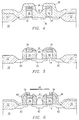
- a masking layer (not shown) is then deposited and patterned on the device.
- An anisotropic etch is performed to define the gate electrodes 20,22 .
- lightly doped drain regions 23 are formed in the substrate 10 .
- a layer of oxide is deposited over the device and sidewall spacers 26 are created along the vertical sidewalls of the gate electrodes 20, 22 , by anisotropically etching the layer.
- Source and drain regions 24 are formed in the substrate 10 .
- a conformal layer 28 of oxide is then deposited over the device, and a via 30 is opened anisotropically etching the device.
- the initial thickness of the insulating layer 18 is decreased.
- the insulating layer 1 is approximately 1-2x10 -7 m (1000 - 2000 angstroms) thick.
- a part of the insulating layer in the via is etched away, leaving that portion of the layer approximately 5x10 -8 m (500 angstroms) thick. Because the insulating layer 18 protects the conductive layer 16 from exposure during formation of the sidewall spacers 26 and the via 30 , a certain minimum thickness is needed to guarantee protection of the gate electrodes 20, 22 .
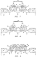
- Figure 3 illustrates formation of the gate electrodes 20, 22 according to the present invention. Isolation regions of field oxide 12 are formed in and on the substrate 10 , and a thin layer of gate oxide 14 is then grown on the exposed areas of the substrate 10 . A conductive layer 16 is deposited over the device, followed by a thin insulating layer 32 . As described in connection with Figures 1 and 2 , the conductive layer 16 can be made from polycrystalline silicon, and is approximately 4x10 -7 m (4000 angstroms) thick. The thin insulating layer 32 can be made from oxide, and have a thickness of approximately 5-1x10 -7 m (500 - 1000 angstroms). A barrier layer 34 is then deposited over the device.
- the barrier layer can be made from any material with a high etch selectivity to the material in the insulating layer 32 .
- the barrier layer 34 can be made from titanium nitride, which has a high etch selectivity to oxide.
- the thickness of the barrier layer can be approximately 3-5x10 -8 m (300 - 500 angstroms).
- a masking layer (not shown) is then deposited and patterned on the device. An anisotropic etch is performed to define the gate electrodes 20, 22 .
- a lightly doped drain region 36 is formed in the substrate 10 .
- a conformal layer 38 of oxide is then deposited over the device.
- Figure 5 illustrates the device after sidewall spacers 40 have been created, and source drain regions 42 have been formed.
- the barrier layer 34 protects the insulating layer 32 and the conductive layer 16 during the anisotropic etch performed to create the sidewall spacers 40 .
- Figures 6 - 8 illustrate several alternative methods which can be used to complete the self-aligned contact.
- a conformal insulating layer 44 is deposited over the device.
- a masking layer (not shown) is deposited and patterned on the device, and an anisotropic etch is performed to open a via 46 .
- the barrier layer 34 again protects the insulating layer 32 and the conductive layer 16 from damage during the etch.
- a portion of the barrier layer 34 is then removed, typically by performing a wet etch.
- the area of the barrier layer 34 closest to the via 46 can be oxidized, thereby capping the end of the remaining barrier layer 34 . As those skilled in the art will appreciate this is especially desirable if the remaining barrier layer 34 is made from a conductive material.
- a contact may be formed by depositing conductive material into the via 46 .
- Figure 7 illustrates an alternative to removing a portion of the barrier layer 34 .
- the barrier layer 34 is made from material that is not conductive, it is possible to leave it on top of the gate electrodes 20 , 22 .
- the barrier layer 34 is made from material that is conductive, it can be oxidized and left on top of the gate electrodes 20 , 22 .
- a conformal insulating layer 44 of oxide is then deposited over the device.
- a masking layer (not shown) is deposited and patterned on the device and an anisotropic etch is performed to open a via 46 .
- the barrier layer 34 again protects the insulating layer 32 and conductive layer 16 from damage during the etch.
- a contact may now be formed by depositing conductive material into the via 46 .
- the barrier layer 34 is completely removed from the gate electrodes 20, 22 before the via 46 is opened. Typically this is done by performing an isotropic etch.
- the conformal insulating layer 44 is then deposited over the device.
- the via 46 is opened, and a contact can be formed by depositing conductive material into the via 46 .
- Figure 9 illustrates the self-aligned contact once these processing steps are complete, and a conductive contact is created by depositing conductive material 48 into the via 46 .
- the conductive material 48 can be, for example, made from silicided polycrystalline silicon.
- This conductive material 48 can be used in conjunction with the processes described in connection with Figures 6 and 7 .
- the thickness of the insulating layer 18 can be reduced from approximately 3.5x10 -7 m (3500 angstroms) to approximately 1x10 -7 m (1000 angstroms) through the use of a barrier layer 34 .
- the total height of the gate electrodes 20, 22 can be reduced from approximately 6x10 -7 m (6000 angstroms) to approximately 4x10 -7 m (4000 angstroms). This reduction in height will improve the topography and make further processing of the device easier and more effective.
Landscapes
- Engineering & Computer Science (AREA)
- Physics & Mathematics (AREA)
- Condensed Matter Physics & Semiconductors (AREA)
- General Physics & Mathematics (AREA)
- Manufacturing & Machinery (AREA)
- Computer Hardware Design (AREA)
- Microelectronics & Electronic Packaging (AREA)
- Power Engineering (AREA)
- Internal Circuitry In Semiconductor Integrated Circuit Devices (AREA)
- Insulated Gate Type Field-Effect Transistor (AREA)
- Electrodes Of Semiconductors (AREA)
- Drying Of Semiconductors (AREA)
Claims (7)
- Struktur bzw. Aufbau für eine integrierte Schaltung, die bzw. der folgendes aufweist:ein Halbleitersubstrat (10);eine Gateelektrode (16);eine erste Isolierschicht (32) mit einer oberen Oberfläche, die auf der oberen Oberfläche der Gateelektrode abgeschieden wird;eine Abschirmschicht bzw. Sperrschicht (34) mit einer oberen Oberfläche, die auf der oberen Oberfläche der ersten Isolierschicht abgeschieden wird;Seitenwand-Abstandseinrichtungen (40), die entlang der vertikalen Seitenwände der Gateelektrode verlaufen; undeine zweite Isolierschicht (44), die oberhalb eines Abschnittes der Gateelektrode positioniert ist, dadurch gekennzeichnet, daß:die Abschirmschicht bzw. Sperrschicht (34) einen metallischen Leiterabschnitt und einen Metalloxid-Isolatorabschnitt aufweist;die zweite Isolierschicht über einem ersten Teil der Abschirmschicht bzw. Sperrschicht liegt; undder Metalloxid-Isolierabschnitt der Abschirmschicht bzw. Sperrschicht die obere Oberfläche des Übrigen bzw des Rests der Abschirmschicht bzw. Sperrschicht ausbildet.
- Struktur bzw. Aufbau für eine integrierte Schaltung, die bzw. der folgendes aufweist:ein Halbleitersubstrat (10);eine Gateelektrode (16);eine erste Isolierschicht (32) mit einer oberen Oberfläche und die auf der oberen Oberfläche der Gateelektrode angeordnet ist;eine Abschirmschicht bzw. Sperrschicht (34) mit einer oberen Oberfläche, die auf der oberen Oberfläche der ersten Isolierschicht angeordnet ist und die weniger als die Gesamtheit der oberen Oberfläche der ersten Isolierschicht abdeckt;Seitenwand-Abstandseinrichtungen (40) entlang der vertikalen Seitenwände der Gateelektrode; undeine zweite Isolierschicht (44), die über einem Abschnitt der Gateelektrode positioniert ist, dadurch gekennzeichnet, daß:die Abschirmschicht bzw. Sperrschicht einen metallischen Leiterabschnitt und einen Metalloxid-Isolatorabschnitt aufweist;die zweite Isolierschicht über der Abschirmschicht bzw. Sperrschicht liegt; undein Endabschnitt der Abschirmschicht bzw. Sperrschicht, die mit einer Seite der zweiten Isolierschicht ausgerichtet ist, von dem Metalloxid-Isolatorabschnitt ausgebildet wird, wobei das Übrige bzw. der Rest der Abschirmschicht bzw. Sperrschicht von dem metallischen Leiterabschnitt ausgebildet wird.
- Struktur bzw. Aufbau nach Anspruch 1 oder Anspruch 2, bei welcher bzw. bei welchem das Abschirmschicht bzw. Sperrschichtmaterial eine hohe Ätzselektivität bezüglich des Materials der ersten Isolierschicht aufweist.
- Struktur bzw. Aufbau, wie in irgendeinem der vorhergehenden Ansprüche beansprucht, bei welcher bzw. bei welchem der metallische Leiterabschnitt Titannitrid aufweist und der Metalloxid-Isolatorabschnitt Titanoxid aufweist.
- Struktur bzw. Aufbau, wie im Anspruch 1 beansprucht ist, bei welcher bzw. bei welchem der Metalloxid-Isolatorabschnitt die obere Oberfläche der gesamten Abschirmschicht bzw. Sperrschicht abdeckt.
- Verfahren zum Ausführen eines selbstausgerichteten bzw. selbstjustierten Kontakts, das die folgenden Schritte aufweist:eine Gateelektrode (16) wird ausgebildet, die eine erste Isolierschicht (32) und eine Abschirmschicht bzw. Sperrschicht (34) aus metallischem leitenden Material auf der oberen Oberfläche davon aufweist;Seitenwand-Abstandseinrichtungen (40) werden entlang der Gateelektrode ausgebildet, wobei die Abschirmschicht bzw. Sperrschicht die Gateelektrode während der Ausbildung der Seitenwand-Abstandseinrichtungen schützt;eine zweite Isolierschicht (44) wird über dem Bauelement abgeschieden; undein Weg durch die zweite Isolierschicht wird geöffnet, dadurch gekennzeichnet, daß:der Öffnungsschritt einen Abschnitt der Oberfläche der Abschirmschicht bzw. Sperrschicht freilegt bzw. belichtet bzw. bestrahlt und dadurch, daß danach der Abschnitt der Abschirmschicht bzw. Sperrschicht in eine Isolierschicht konvertiert wird, wodurch die Abschirmschicht bzw. Sperrschicht einen Metalloxid-Isolatorabschnitt und einen metallischen Leiterabschnitt aufweist.
- Verfahren zum Ausbilden eines selbstausgerichteten bzw. selbstjustierten Kontaktes, das die folgenden Schritte aufweist:eine Gateelektrode (16) wird ausgebildet, die eine erste Isolierschicht (32) und eine Abschirmschicht bzw. Sperrschicht (34) eines metallischen leitenden Materials auf der oberen Oberfläche davon aufweist; (?)Seitenwand-Abstandseinrichtungen (40) werden entlang der Gateelektrode ausgebildet, wobei die Abschirmschicht bzw. Sperrschicht die Gateelektrode während der Ausbildung der Seitenwand-Abstandseinrichtungen schützt;eine zweite Isolierschicht (44) wird über dem Bauelement abgeschieden; undein Weg durch die zweite Isolierschicht wird geöffnet, dadurch gekennzeichnet, daß:ein Abschnitt bzw. Teil der Abschirmschicht bzw. Sperrschicht entfernt wird und ein Abschnitt der verbleibenden Abschirmschicht bzw. Sperrschicht in eine isolierende Fläche nach der Ausbildung des Weges durch Oxidieren eines Abschnittes bzw. Teiles der verbleibenden Abschirmschicht bzw. Sperrschicht konvertiert bzw. umgewandelt wird.
Applications Claiming Priority (2)
| Application Number | Priority Date | Filing Date | Title |
|---|---|---|---|
| US786019 | 1985-10-10 | ||
| US78601991A | 1991-10-31 | 1991-10-31 |
Publications (3)
| Publication Number | Publication Date |
|---|---|
| EP0540276A2 EP0540276A2 (de) | 1993-05-05 |
| EP0540276A3 EP0540276A3 (de) | 1994-02-23 |
| EP0540276B1 true EP0540276B1 (de) | 1997-09-24 |
Family
ID=25137358
Family Applications (1)
| Application Number | Title | Priority Date | Filing Date |
|---|---|---|---|
| EP92309796A Expired - Lifetime EP0540276B1 (de) | 1991-10-31 | 1992-10-26 | Herstellungsverfahren eines selbstjustierenden Kontakts |
Country Status (4)
| Country | Link |
|---|---|
| US (2) | US5369303A (de) |
| EP (1) | EP0540276B1 (de) |
| JP (1) | JPH05283359A (de) |
| DE (1) | DE69222390T2 (de) |
Families Citing this family (19)
| Publication number | Priority date | Publication date | Assignee | Title |
|---|---|---|---|---|
| US5880022A (en) * | 1991-12-30 | 1999-03-09 | Lucent Technologies Inc. | Self-aligned contact window |
| JP2925416B2 (ja) * | 1992-11-09 | 1999-07-28 | 株式会社東芝 | 半導体集積回路装置の製造方法 |
| US5679982A (en) * | 1993-02-24 | 1997-10-21 | Intel Corporation | Barrier against metal diffusion |
| KR970010685B1 (ko) * | 1993-10-30 | 1997-06-30 | 삼성전자 주식회사 | 누설전류가 감소된 박막 트랜지스터 및 그 제조방법 |
| KR0141950B1 (ko) * | 1994-12-22 | 1998-06-01 | 문정환 | 반도체소자의 제조방법 |
| US5654570A (en) * | 1995-04-19 | 1997-08-05 | International Business Machines Corporation | CMOS gate stack |
| US5960318A (en) * | 1995-10-27 | 1999-09-28 | Siemens Aktiengesellschaft | Borderless contact etch process with sidewall spacer and selective isotropic etch process |
| US5773341A (en) | 1996-01-18 | 1998-06-30 | Micron Technology, Inc. | Method of making capacitor and conductive line constructions |
| US5861340A (en) * | 1996-02-15 | 1999-01-19 | Intel Corporation | Method of forming a polycide film |
| US5808362A (en) * | 1996-02-29 | 1998-09-15 | Motorola, Inc. | Interconnect structure and method of forming |
| JP3795634B2 (ja) * | 1996-06-19 | 2006-07-12 | 株式会社東芝 | 半導体装置の製造方法 |
| TW409361B (en) * | 1999-05-13 | 2000-10-21 | Mosel Vitelic Inc | Self-aligned contact process |
| US6461743B1 (en) | 2000-08-17 | 2002-10-08 | Louisiana-Pacific Corp. | Smooth-sided integral composite engineered panels and methods for producing same |
| US6940134B2 (en) * | 2002-07-02 | 2005-09-06 | International Business Machines Corporation | Semiconductor with contact contacting diffusion adjacent gate electrode |
| US20060058854A1 (en) * | 2004-09-14 | 2006-03-16 | Scimed Life Systems, Inc. | Method for stimulating neural tissue in response to a sensed physiological event |
| US7642152B2 (en) * | 2005-09-07 | 2010-01-05 | United Microelectronics Corp. | Method of fabricating spacers and cleaning method of post-etching and semiconductor device |
| DE102009047891B4 (de) * | 2009-09-30 | 2012-02-23 | GLOBALFOUNDRIES Dresden Module One Ltd. Liability Company & Co. KG | Verfahren zur Herstellung eines Transistors mit verbesserten Füllbedingungen in einem Austauschgateverfahren durch Eckenverrundung vor dem vollständigen Entfernen eines Platzhaltermaterials |
| KR102167625B1 (ko) * | 2013-10-24 | 2020-10-19 | 삼성전자주식회사 | 반도체 장치 및 그 제조 방법 |
| US9548366B1 (en) * | 2016-04-04 | 2017-01-17 | Taiwan Semiconductor Manufacturing Company, Ltd. | Self aligned contact scheme |
Family Cites Families (8)
| Publication number | Priority date | Publication date | Assignee | Title |
|---|---|---|---|---|
| US4743564A (en) * | 1984-12-28 | 1988-05-10 | Kabushiki Kaisha Toshiba | Method for manufacturing a complementary MOS type semiconductor device |
| US4826781A (en) * | 1986-03-04 | 1989-05-02 | Seiko Epson Corporation | Semiconductor device and method of preparation |
| US4855798A (en) * | 1986-12-19 | 1989-08-08 | Texas Instruments Incorporated | Semiconductor and process of fabrication thereof |
| KR920007787B1 (ko) * | 1987-06-09 | 1992-09-17 | 세이꼬 엡슨 가부시끼가이샤 | 반도체 장치 및 그 제조방법 |
| US4786609A (en) * | 1987-10-05 | 1988-11-22 | North American Philips Corporation, Signetics Division | Method of fabricating field-effect transistor utilizing improved gate sidewall spacers |
| US4922311A (en) * | 1987-12-04 | 1990-05-01 | American Telephone And Telegraph Company | Folded extended window field effect transistor |
| JPH0783066B2 (ja) * | 1989-08-11 | 1995-09-06 | 株式会社東芝 | 半導体装置の製造方法 |
| US5043790A (en) * | 1990-04-05 | 1991-08-27 | Ramtron Corporation | Sealed self aligned contacts using two nitrides process |
-
1992
- 1992-10-26 EP EP92309796A patent/EP0540276B1/de not_active Expired - Lifetime
- 1992-10-26 DE DE69222390T patent/DE69222390T2/de not_active Expired - Fee Related
- 1992-11-02 JP JP4293603A patent/JPH05283359A/ja active Pending
-
1993
- 1993-09-02 US US08/116,050 patent/US5369303A/en not_active Expired - Lifetime
-
1994
- 1994-08-19 US US08/293,140 patent/US5500382A/en not_active Expired - Lifetime
Also Published As
| Publication number | Publication date |
|---|---|
| DE69222390T2 (de) | 1998-03-19 |
| US5500382A (en) | 1996-03-19 |
| EP0540276A2 (de) | 1993-05-05 |
| JPH05283359A (ja) | 1993-10-29 |
| US5369303A (en) | 1994-11-29 |
| EP0540276A3 (de) | 1994-02-23 |
| DE69222390D1 (de) | 1997-10-30 |
Similar Documents
| Publication | Publication Date | Title |
|---|---|---|
| EP0540276B1 (de) | Herstellungsverfahren eines selbstjustierenden Kontakts | |
| US5321211A (en) | Integrated circuit via structure | |
| US6010935A (en) | Self aligned contacts | |
| US6495900B1 (en) | Insulator for electrical structure | |
| US5206183A (en) | Method of forming a bit line over capacitor array of memory cells | |
| US6285073B1 (en) | Contact structure and method of formation | |
| US6232647B1 (en) | Air gap with borderless contact | |
| US5885883A (en) | Methods of forming trench-based isolation regions with reduced susceptibility to edge defects | |
| EP0523856A2 (de) | Verfahren zur Herstellung von einer Kontaktbohrung für Mehrschichtverbindungen in integrierten Schaltungen | |
| US5593920A (en) | Method for forming contact structures in integrated circuits | |
| US5593921A (en) | Method of forming vias | |
| US5459354A (en) | Semiconductor device with improved insulation of wiring structure from a gate electrode | |
| KR100287179B1 (ko) | 비트라인를포함하는반도체장치및그제조방법 | |
| EP0426305A1 (de) | Methode zum Ätzen von Fensterscheiben verschiedener Tiefe | |
| US5872056A (en) | Semiconductor processing methods of forming self-aligned contact openings | |
| US6060765A (en) | Semiconductor device and a method of manufacturing the same | |
| US5989987A (en) | Method of forming a self-aligned contact in semiconductor fabrications | |
| EP0526244B1 (de) | Verfahren zur Herstellung eines vergrabenen Kontaktes aus Polysilizium | |
| US6093627A (en) | Self-aligned contact process using silicon spacers | |
| US5589418A (en) | Method of forming a polysilicon buried contact | |
| US6458680B2 (en) | Method of fabricating contact pads of a semiconductor device | |
| US6483153B1 (en) | Method to improve LDD corner control with an in-situ film for local interconnect processing | |
| JP2000003961A (ja) | 集積回路およびその製造方法 | |
| JP3449137B2 (ja) | 半導体装置の製造方法 | |
| US5847457A (en) | Structure and method of forming vias |
Legal Events
| Date | Code | Title | Description |
|---|---|---|---|
| PUAI | Public reference made under article 153(3) epc to a published international application that has entered the european phase |
Free format text: ORIGINAL CODE: 0009012 |
|
| AK | Designated contracting states |
Kind code of ref document: A2 Designated state(s): DE FR GB IT |
|
| PUAL | Search report despatched |
Free format text: ORIGINAL CODE: 0009013 |
|
| RHK1 | Main classification (correction) |
Ipc: H01L 21/60 |
|
| AK | Designated contracting states |
Kind code of ref document: A3 Designated state(s): DE FR GB IT |
|
| 17P | Request for examination filed |
Effective date: 19940818 |
|
| 17Q | First examination report despatched |
Effective date: 19951129 |
|
| GRAG | Despatch of communication of intention to grant |
Free format text: ORIGINAL CODE: EPIDOS AGRA |
|
| GRAH | Despatch of communication of intention to grant a patent |
Free format text: ORIGINAL CODE: EPIDOS IGRA |
|
| GRAH | Despatch of communication of intention to grant a patent |
Free format text: ORIGINAL CODE: EPIDOS IGRA |
|
| GRAA | (expected) grant |
Free format text: ORIGINAL CODE: 0009210 |
|
| AK | Designated contracting states |
Kind code of ref document: B1 Designated state(s): DE FR GB IT |
|
| PGFP | Annual fee paid to national office [announced via postgrant information from national office to epo] |
Ref country code: FR Payment date: 19971009 Year of fee payment: 6 |
|
| PGFP | Annual fee paid to national office [announced via postgrant information from national office to epo] |
Ref country code: GB Payment date: 19971017 Year of fee payment: 6 |
|
| REF | Corresponds to: |
Ref document number: 69222390 Country of ref document: DE Date of ref document: 19971030 |
|
| PGFP | Annual fee paid to national office [announced via postgrant information from national office to epo] |
Ref country code: DE Payment date: 19971031 Year of fee payment: 6 |
|
| ITF | It: translation for a ep patent filed |
Owner name: PORTA CHECCACCI E BOTTI S.R.L. |
|
| ET | Fr: translation filed | ||
| PLBE | No opposition filed within time limit |
Free format text: ORIGINAL CODE: 0009261 |
|
| STAA | Information on the status of an ep patent application or granted ep patent |
Free format text: STATUS: NO OPPOSITION FILED WITHIN TIME LIMIT |
|
| 26N | No opposition filed | ||
| PG25 | Lapsed in a contracting state [announced via postgrant information from national office to epo] |
Ref country code: GB Free format text: LAPSE BECAUSE OF NON-PAYMENT OF DUE FEES Effective date: 19981026 |
|
| GBPC | Gb: european patent ceased through non-payment of renewal fee |
Effective date: 19981026 |
|
| PG25 | Lapsed in a contracting state [announced via postgrant information from national office to epo] |
Ref country code: FR Free format text: LAPSE BECAUSE OF NON-PAYMENT OF DUE FEES Effective date: 19990630 |
|
| REG | Reference to a national code |
Ref country code: FR Ref legal event code: ST |
|
| PG25 | Lapsed in a contracting state [announced via postgrant information from national office to epo] |
Ref country code: DE Free format text: LAPSE BECAUSE OF NON-PAYMENT OF DUE FEES Effective date: 19990803 |
|
| PG25 | Lapsed in a contracting state [announced via postgrant information from national office to epo] |
Ref country code: IT Free format text: LAPSE BECAUSE OF NON-PAYMENT OF DUE FEES Effective date: 20051026 |