EP0531426B1 - Procede automatise pour la fabrication de dispositifs repondeurs - Google Patents
Procede automatise pour la fabrication de dispositifs repondeurs Download PDFInfo
- Publication number
- EP0531426B1 EP0531426B1 EP91910963A EP91910963A EP0531426B1 EP 0531426 B1 EP0531426 B1 EP 0531426B1 EP 91910963 A EP91910963 A EP 91910963A EP 91910963 A EP91910963 A EP 91910963A EP 0531426 B1 EP0531426 B1 EP 0531426B1
- Authority
- EP
- European Patent Office
- Prior art keywords
- leads
- bobbin
- wire
- lead
- leadframe
- Prior art date
- Legal status (The legal status is an assumption and is not a legal conclusion. Google has not performed a legal analysis and makes no representation as to the accuracy of the status listed.)
- Expired - Lifetime
Links
- 238000000034 method Methods 0.000 title claims abstract description 51
- 238000004519 manufacturing process Methods 0.000 title claims abstract description 25
- 238000004804 winding Methods 0.000 claims abstract description 19
- 238000000465 moulding Methods 0.000 claims description 4
- 238000003909 pattern recognition Methods 0.000 claims description 3
- 239000000463 material Substances 0.000 claims description 2
- 230000003190 augmentative effect Effects 0.000 abstract description 8
- 238000001721 transfer moulding Methods 0.000 abstract description 4
- 229910052709 silver Inorganic materials 0.000 abstract description 3
- 239000004332 silver Substances 0.000 abstract description 3
- 238000012938 design process Methods 0.000 abstract 1
- 239000004065 semiconductor Substances 0.000 abstract 1
- 230000000712 assembly Effects 0.000 description 4
- 238000000429 assembly Methods 0.000 description 4
- 239000004593 Epoxy Substances 0.000 description 3
- 239000003990 capacitor Substances 0.000 description 3
- 238000002955 isolation Methods 0.000 description 3
- 238000009966 trimming Methods 0.000 description 3
- BQCADISMDOOEFD-UHFFFAOYSA-N Silver Chemical compound [Ag] BQCADISMDOOEFD-UHFFFAOYSA-N 0.000 description 2
- 230000008878 coupling Effects 0.000 description 2
- 238000010168 coupling process Methods 0.000 description 2
- 238000005859 coupling reaction Methods 0.000 description 2
- 238000001514 detection method Methods 0.000 description 2
- 239000004033 plastic Substances 0.000 description 2
- RYGMFSIKBFXOCR-UHFFFAOYSA-N Copper Chemical compound [Cu] RYGMFSIKBFXOCR-UHFFFAOYSA-N 0.000 description 1
- XUIMIQQOPSSXEZ-UHFFFAOYSA-N Silicon Chemical compound [Si] XUIMIQQOPSSXEZ-UHFFFAOYSA-N 0.000 description 1
- 239000000853 adhesive Substances 0.000 description 1
- 230000001070 adhesive effect Effects 0.000 description 1
- XAGFODPZIPBFFR-UHFFFAOYSA-N aluminium Chemical compound [Al] XAGFODPZIPBFFR-UHFFFAOYSA-N 0.000 description 1
- 229910052782 aluminium Inorganic materials 0.000 description 1
- 239000011248 coating agent Substances 0.000 description 1
- 238000000576 coating method Methods 0.000 description 1
- 238000010276 construction Methods 0.000 description 1
- 238000005520 cutting process Methods 0.000 description 1
- 230000004069 differentiation Effects 0.000 description 1
- 238000004146 energy storage Methods 0.000 description 1
- 238000005516 engineering process Methods 0.000 description 1
- 239000011521 glass Substances 0.000 description 1
- 239000003292 glue Substances 0.000 description 1
- PCHJSUWPFVWCPO-UHFFFAOYSA-N gold Chemical compound [Au] PCHJSUWPFVWCPO-UHFFFAOYSA-N 0.000 description 1
- 229910052737 gold Inorganic materials 0.000 description 1
- 239000010931 gold Substances 0.000 description 1
- 230000001939 inductive effect Effects 0.000 description 1
- 230000003993 interaction Effects 0.000 description 1
- 238000004801 process automation Methods 0.000 description 1
- 238000004080 punching Methods 0.000 description 1
- 238000000926 separation method Methods 0.000 description 1
- 229910052710 silicon Inorganic materials 0.000 description 1
- 239000010703 silicon Substances 0.000 description 1
- 229910000679 solder Inorganic materials 0.000 description 1
- 239000007787 solid Substances 0.000 description 1
- 229920001169 thermoplastic Polymers 0.000 description 1
- 239000004416 thermosoftening plastic Substances 0.000 description 1
Images


Classifications
-
- G—PHYSICS
- G06—COMPUTING; CALCULATING OR COUNTING
- G06K—GRAPHICAL DATA READING; PRESENTATION OF DATA; RECORD CARRIERS; HANDLING RECORD CARRIERS
- G06K19/00—Record carriers for use with machines and with at least a part designed to carry digital markings
- G06K19/06—Record carriers for use with machines and with at least a part designed to carry digital markings characterised by the kind of the digital marking, e.g. shape, nature, code
- G06K19/067—Record carriers with conductive marks, printed circuits or semiconductor circuit elements, e.g. credit or identity cards also with resonating or responding marks without active components
- G06K19/07—Record carriers with conductive marks, printed circuits or semiconductor circuit elements, e.g. credit or identity cards also with resonating or responding marks without active components with integrated circuit chips
- G06K19/077—Constructional details, e.g. mounting of circuits in the carrier
- G06K19/07749—Constructional details, e.g. mounting of circuits in the carrier the record carrier being capable of non-contact communication, e.g. constructional details of the antenna of a non-contact smart card
- G06K19/07758—Constructional details, e.g. mounting of circuits in the carrier the record carrier being capable of non-contact communication, e.g. constructional details of the antenna of a non-contact smart card arrangements for adhering the record carrier to further objects or living beings, functioning as an identification tag
-
- G—PHYSICS
- G01—MEASURING; TESTING
- G01V—GEOPHYSICS; GRAVITATIONAL MEASUREMENTS; DETECTING MASSES OR OBJECTS; TAGS
- G01V15/00—Tags attached to, or associated with, an object, in order to enable detection of the object
-
- G—PHYSICS
- G06—COMPUTING; CALCULATING OR COUNTING
- G06K—GRAPHICAL DATA READING; PRESENTATION OF DATA; RECORD CARRIERS; HANDLING RECORD CARRIERS
- G06K19/00—Record carriers for use with machines and with at least a part designed to carry digital markings
- G06K19/06—Record carriers for use with machines and with at least a part designed to carry digital markings characterised by the kind of the digital marking, e.g. shape, nature, code
- G06K19/067—Record carriers with conductive marks, printed circuits or semiconductor circuit elements, e.g. credit or identity cards also with resonating or responding marks without active components
- G06K19/07—Record carriers with conductive marks, printed circuits or semiconductor circuit elements, e.g. credit or identity cards also with resonating or responding marks without active components with integrated circuit chips
- G06K19/077—Constructional details, e.g. mounting of circuits in the carrier
- G06K19/07749—Constructional details, e.g. mounting of circuits in the carrier the record carrier being capable of non-contact communication, e.g. constructional details of the antenna of a non-contact smart card
- G06K19/07773—Antenna details
- G06K19/07777—Antenna details the antenna being of the inductive type
- G06K19/07779—Antenna details the antenna being of the inductive type the inductive antenna being a coil
- G06K19/07781—Antenna details the antenna being of the inductive type the inductive antenna being a coil the coil being fabricated in a winding process
-
- H—ELECTRICITY
- H01—ELECTRIC ELEMENTS
- H01F—MAGNETS; INDUCTANCES; TRANSFORMERS; SELECTION OF MATERIALS FOR THEIR MAGNETIC PROPERTIES
- H01F17/00—Fixed inductances of the signal type
- H01F17/02—Fixed inductances of the signal type without magnetic core
-
- H—ELECTRICITY
- H01—ELECTRIC ELEMENTS
- H01F—MAGNETS; INDUCTANCES; TRANSFORMERS; SELECTION OF MATERIALS FOR THEIR MAGNETIC PROPERTIES
- H01F41/00—Apparatus or processes specially adapted for manufacturing or assembling magnets, inductances or transformers; Apparatus or processes specially adapted for manufacturing materials characterised by their magnetic properties
- H01F41/02—Apparatus or processes specially adapted for manufacturing or assembling magnets, inductances or transformers; Apparatus or processes specially adapted for manufacturing materials characterised by their magnetic properties for manufacturing cores, coils, or magnets
-
- Y—GENERAL TAGGING OF NEW TECHNOLOGICAL DEVELOPMENTS; GENERAL TAGGING OF CROSS-SECTIONAL TECHNOLOGIES SPANNING OVER SEVERAL SECTIONS OF THE IPC; TECHNICAL SUBJECTS COVERED BY FORMER USPC CROSS-REFERENCE ART COLLECTIONS [XRACs] AND DIGESTS
- Y10—TECHNICAL SUBJECTS COVERED BY FORMER USPC
- Y10T—TECHNICAL SUBJECTS COVERED BY FORMER US CLASSIFICATION
- Y10T29/00—Metal working
- Y10T29/49—Method of mechanical manufacture
- Y10T29/49002—Electrical device making
- Y10T29/49007—Indicating transducer
-
- Y—GENERAL TAGGING OF NEW TECHNOLOGICAL DEVELOPMENTS; GENERAL TAGGING OF CROSS-SECTIONAL TECHNOLOGIES SPANNING OVER SEVERAL SECTIONS OF THE IPC; TECHNICAL SUBJECTS COVERED BY FORMER USPC CROSS-REFERENCE ART COLLECTIONS [XRACs] AND DIGESTS
- Y10—TECHNICAL SUBJECTS COVERED BY FORMER USPC
- Y10T—TECHNICAL SUBJECTS COVERED BY FORMER US CLASSIFICATION
- Y10T29/00—Metal working
- Y10T29/49—Method of mechanical manufacture
- Y10T29/49002—Electrical device making
- Y10T29/4902—Electromagnet, transformer or inductor
- Y10T29/49071—Electromagnet, transformer or inductor by winding or coiling
Definitions
- the present invention relates to an automated method for manufacturing a passive transponder device.
- the present invention relates to the automated production of transponder devices and, still more particularly, to an automated method of manufacturing alternatively sized passive transponder devices using a single tape leadframe design and a bobbin for assembling the transponder.
- Transponders have been used for identification purposes for many years in the detection and identification of animate and inanimate objects. Initially, an operator, using a hand-held or other type of transmitter/reader, directs a beam of energy toward the transponder. This energy is usually in the form of an electromagnetic radio wave and acts to charge a minute capacitor, or similar energy storage component, within the transponder device. An integrated circuit, also a component of the transponder, contains identification information pertinent to a particular application. When activated by the electromagnetic wave, the information stored on this chip is electromagnetically retransmitted and can be received by an appropriate receiver thus enabling identification of the transponder device carrier.
- Document EP-B1-0 526 484 (belonging to the prior art according to Article 54(3) EPC) discloses a process for assembly of an air-core coil on a printed circuit board as used for credit cards or wireless detection systems. This prior art process teaches to place a printed circuit board on a winding machine, to subsequently produce a winding on the printed circuit board surface opposite the printed circuit installed, to glue the winding on the printed circuit board and to solder the ends of the wound wire on metallized tracks on the printed circuit previously applied to the board surface.
- Another object of the present invention is to provide a method of the type described wherein the ends of the conductive wire used in core winding can be terminated by conductive coupling to the leads of the leadframe using a fully automated bonding process.
- the claimed method comprises to first prepare a specially designed leadframe assembly from which multiple parts of varying sizes can be cut. Electrical components are bonded and wired to each individual site or frame of the leadframe, and this lead-die assembly is then encapsulated in a thermoplastic shell. The leadframe is then trimmed in a manner consistent with the size of the transponder in which an individual lead-die assembly is to be used, and an appropriate bobbin is attached at each distinct trimmed site. The individual bobbins and lead-die assemblies are then physically singulated from the leadframe, and one end of the core wire is attached to a first of the augmented leads using an automated wire tracking and bonding process. The bobbin core is subsequently wound with the core wire using an automated fly-winding means, after which the wire is terminated by connection to the second augmented lead. The assembled transponder is then packaged, preferably in a glass or plastic housing.
- Fig. 1 is a top plan view of a portion of the specially designed leadframe used in transponder production in accordance with the method of the present invention.
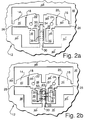
- Fig. 2a is a top plan view of an individual site of the leadframe shown in Fig. 1, illustrating the die bonding areas.
- Fig. 2b is a top plan view of an individual site of the leadframe shown in Fig. 1, illustrating chip placement and electrical connection.
- Fig. 3a is a side elevational view of the singulated molded cap with the lead-die assembly enclosed, illustrating a first alternative lead-size embodiment in accordance with the method of the present invention.
- Fig. 3b is a side elevational view of the singulated molded cap with the lead-die assembly enclosed, illustrating a second alternative lead size embodiment in accordance with the method of the present invention.
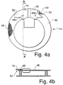
- Fig. 4a is a partially broken top plan view of the singulated cap and lead-die assembly as it appears attached to the bobbin.
- Fig. 4b is a cross-sectional view of the illustration in Fig. 4a, taken along the line AA.
- leadframe 10 comprises an array of individual leadframe sites 12 arranged such that a number of individual sites are included within the confines of a single leadframe.
- the leadframe could be a tape instead of a sheet.
- FIG. 2a shown is the detail of an individual site 12 of leadframe 10.
- Augmented leads 14 and 16 are provided, with rectangular cut-outs 18 and 20, respectively, therein, and holes 22 and 24, respectively, therethrough.
- the body of the leads 14 is connected to the leadframe 10 by frame supports 26, 28 and 30.
- An important characteristic of leads 14 and 16 is their augmented width, which effectively provides an expanded surface area to which electrical connections can be made. As described below, this feature facilitates automated wire-to-lead connection capabilities that have heretofore been impracticable.
- the transponder shown in the figures includes three circuit devices: a chip with identifying information 33; a zener protection chip 35; and a capacitor chip 37 (all shown in Fig. 2b). Alternatively, these functional elements could be combined in a single integrated circuit.
- the circuit devices are attached to the leadframe 10 with epoxy. This is a fully automated process using a bonding machine and technique known in the art. Referring again to Fig. 2a, when the leadframe 10 is in the appropriate position within the bonding machine, the circuit devices are automatically deposited at each of the predetermined bonding sites 32, 34 and 36. This process is repeated for each of the individual sites 12, until the entire leadframe 10 is similarly prepared. The individual sites 12 may be prepared simultaneously.
- the bonding machine automatically places the three chips 33,35,37 in their proper positions on bonding sites 32, 34 and 36, as shown in Fig. 2b.
- the lead frames 10, with chips 33,35,37 or "die” attached can be loaded into a magazine and cured in bulk, in a convection oven, or cured individually in an ultra-violet curing tunnel oven. After curing, the die-loaded leadframes 10 are ready for the next step in the production process.
- the next step in the method of the present invention is the wire bonding of circuit devices 33 and 35 to the leadframe 10.
- four fine gold wires 60-63 are connected from the aluminum pads on the silicon dice 33 and 35 to the electrical connections on the leadframe 10.
- a first connecting wire 60 couples identification chip 33 to left lead 14, and a second connecting wire 61 couples chip 33 to right lead 16.
- a third connecting wire 62 couples Zener protection chip 35 to lead 14, and a fourth connecting wire 63 couples chip 35 to lead 16.
- the wire bonding process is automatic, using pattern recognition, and is simplified by the augmented width of the leads 14,16.
- Capacitor chip 37 is electrically connected to the leadframe 10, in a position as shown in Fig. 2b, by use of the previously applied conductive die-bonding epoxy.
- the next step in the method in accordance with the present invention is the transfer molding of the leadframes 10 with die attached, and wire bonds complete.
- This is a common manufacturing technique, and thus will be described here only in general terms.
- the leadframes 10, prepared as described above, are loaded into magazines and inserted into a molding machine.
- Thermal-setting plastic is molded over the body of the leadframe-die assembly in order to protect the delicate electronics and fine-wire connections from physical and electrical damage.
- Part of the extraneous molded pot, runners and gates produced during the molding process can be removed at this time. However, this is normally done during the trimming and singulation operation, described below.
- the molding operation effectively produces a cap 41, shown in Figs.
- the next step in the method in accordance with the present invention is the electrical isolation of the individual sites 12 from leadframe 10.
- electrical isolation is accomplished by trimming the frame supports 26, 28 and 30 from the main body of the leadframe 10. This can be done manually, or can be automated using techniques well known in the industry.
- the next step in the method according to the present invention is the singulation trimming operation. Singulation is achieved physically by using an automated mechanical punching device which stamps the cap 41 and leads 14,16 from the body of the leadframe 10. It is at this point in the overall manufacturing process that differentiation is made between the differently sized transponder devices.
- a first larger sized transponder device is formed by singulating the cap-enclosed lead-die assembly from the molded runners and gates at the same position as that in which electrical isolation was performed, at frame supports 26 and 28.
- leads 14 and 16 extend fully to the internal edge of site 12, to the position of previously connected supports 26 and 28. This allows the maximum surface area of the leads 14,16 to be utilized for the bonding of the coil wire ends.
- a second smaller sized transponder device is formed by singulating the cap-enclosed lead-die assembly from the molded runners and gates through the center of rectangular cut-outs 18 and 20, and parallel to the longitudinal axes thereof.
- the leads 14,16 would be singulated by cutting through the cut-outs 18 and 20 such that only the material at the extreme ends thereof would actually be cut.
- This leadframe design facilitates accuracy and consistency in the singulation process, in addition to making the actual physical separation easier to accomplish.
- the remaining surface area of the leads 14,16 provide access for the connection of the coil wire ends.
- the individual cap-enclosed lead-die assemblies of each site 12 are now separated from the main body of the leadframe 10, and are ready for attachment to bobbins 44, as described below.
- Figs. 3a and 3b shown are side elevational views of the alternatively sized cap-enclosed lead-die assemblies, as formed using the above-described processes.
- Fig. 3a shows the larger assembly with the full surface area of leads 14 and 16 intact.
- Fig. 3b is representative of the smaller cap-enclosed lead-die assembly, which provides the shortened leads 14 and 16 for the wire bonding. In either case, the width of leads 14 and 16 is sufficient to accommodate fully automated connection of the fine core wire thereto.
- bobbin 44 with the above-described fully singulated cap-enclosed lead-die assembly attached thereto.
- An individual bobbin 44 is disposed in a predetermined position relative to an individual cap-enclosed lead-die assembly.
- the bobbins 44 include one or more connecting and positioning pins 46, shown in Fig. 4b, which project perpendicularly upward from a flattened outer surface 48 of the bobbin 44.
- each bobbin 44 is provided with two separate positioning and connecting pins 46a and 46b, shown in Fig. 4b, for connection to leads 14 and 16, respectively.
- the pins 46a and 46b are automatically positioned within the holes 22 and 24 of leads 14 and 16, respectively, such that the leads lie flat against the upper surface 48 of the bobbin 44, and the pins 46a,46b extend therethrough.
- Pins 46a and 46b can be used solely for positioning of the bobbin 44 against the leads 14,16, or they can also be used as a means of connecting the leads 14,16 and bobbin 44 together. If the pins 46a,46b are used solely for positioning, the leads 14,16 and bobbin 44 can be connected together in any suitable fashion, such as with epoxy or a like adhesive. In this manner, the pins 46a,46b would provide a means for correctly orienting the bobbin 44 against the leads 14,16 via alignment through holes 22 and 24. Alternatively, the pins 46a,46b can be used for both positioning and connection of the bobbin 44 to the leads 14,16, by heat riveting or otherwise attaching the pins 46a,46b within holes, such that a solid and sturdy connection is made therebetween.
- the inner and outer radii of bobbin 44 are not symmetrically concentric. That is, the central radial axis of the outer diameter of surface 48 is parallel to, but not collinear with, the central radial axis of the inner diameter of surface 48.
- This offset provides for a greater surface area on one portion of surface 48 which in turn accommodates connecting pins 46a and 46b, and connection cut-outs 50 and 52 (the latter being represented by the phantom line in Fig. 4a).
- These cut-outs 50,52 are included to accommodate the twin wire termination process described in further detail below.
- Fig. 4b is a cross-sectional view of the bobbin 44 as it appears when attached to leads 14 and 16, via the connecting pins 46a and 46b. Note that lead 14 extends over cut-out 52 such that the bottom surface thereof is exposed to the bobbin core winding area. Lead 16, in a similar manner, extends over cut-out 50 such that the bottom surface of lead 16 is also exposed to the bobbin core winding area (not shown in Fig. 4b).
- the next step in the method of the present invention is coil winding and wire-to-lead attachment. Because of the fine size of the wire used in most transponder devices, i.e., in the order of a few to several microns, automated coupling of the wire ends to the die has been heretofore impracticable. In the prior art methods, manual wire manipulation and bonding is necessary to ensure that the proper connections are effectively made. However, according to the method of the present invention, these connections can be automated. By continuously dispensing the wire from a relatively small syringe-like tube, constant tracking of wire placement is realized during the full operation of lead bonding and coil winding. This tracking, in conjunction with the augmented surface area of the exposed leads 14,16, accommodates full process automation, as described below.
- wire 49 is held within the syringe-like tube and is placed against the bottom surface of lead 14, which is exposed by cut-out 52.
- An electrode automatically descends and presses wire 49 against this lead 14, liquefying a thin coating of silver thereon.
- the silver solidifies and physically bonds the wire 49 to the lead 14. Because of the greater surface area of the lead 14, as compared to a bonding pad directly on the die, and because the wire position is precisely known, this bonding process can be performed accurately and effectively, without operator intervention.
- alternative means for attaching the wire 49 to the lead 14 may be used.
- a flywheel is used for automatically "fly-winding" wire 49 around the center portion of the bobbin 44 at a speed between 30,000 to 50,000 rpm. Winding at this speed is made possible by the lead bonding technique employed in the production process, and by the use of the narrow tube for the wire dispensation.
- the free wire end still held within the tube, is bonded to the lead 16, the bottom surface of which is exposed by cut-out 50.
- the wire-dispensing tube is placed next to the lead 16, and an electrode automatically descends and bonds the wire 49 to the exposed augmented lead 16. This again is made possible because the wire position is precisely known due to use of the syringe-like dispenser, and because of the expanded surface area available for bonding on the lead 16.
Landscapes
- Engineering & Computer Science (AREA)
- Microelectronics & Electronic Packaging (AREA)
- General Physics & Mathematics (AREA)
- Physics & Mathematics (AREA)
- Theoretical Computer Science (AREA)
- Computer Hardware Design (AREA)
- Power Engineering (AREA)
- Computer Networks & Wireless Communication (AREA)
- Geophysics (AREA)
- Manufacturing & Machinery (AREA)
- General Life Sciences & Earth Sciences (AREA)
- Life Sciences & Earth Sciences (AREA)
- Wire Bonding (AREA)
- Lead Frames For Integrated Circuits (AREA)
- Radar Systems Or Details Thereof (AREA)
- Near-Field Transmission Systems (AREA)
Abstract
Claims (9)
- Procédé automatique de fabrication d'un dispositif répondeur passif, comprenant les étapes consistant à :1.1 préparer un cadre conducteur (10) comprenant une pluralité de sites de montage individuels (12) ayant chacun une pluralité de conducteurs (14, 16) ;1.2 lier un dispositif d'identification électronique composé d'au moins une puce de circuit intégré (33, 35, 37) à chacun desdits sites (12) ;1.3 connecter électriquement chacun desdits dispositifs d'identification électroniques auxdits conducteurs (14, 16) en chacun desdits sites (12) ;1.4 mouler un capuchon (41) autour de chacun desdits dispositifs d'identification électroniques et de premières parties des conducteurs (14, 16) sur le site (12) en sorte que des deuxièmes parties des conducteurs (14, 16) dépassent dudit capuchon (41) ;1.5 détacher les deuxièmes parties desdits conducteurs (14, 16), pour dissocier ainsi chacun desdits capuchons (41) dudit cadre conducteur (10) ;1.6 attacher une bobine (44) à ladite deuxième partie desdits conducteurs (14, 16) dépassant de chacun desdits capuchons (41) ;1.7 enrouler un fil conducteur (49) autour de chacune desdites bobines (44) ; et1.8 connecter de manière conductrice ledit fil (49) aux conducteurs correspondants (14, 16).
- Procédé selon la revendication 1, caractérisé en ce que chacun desdits dispositifs d'identification électroniques est connecté de manière conductrice auxdits conducteurs (14, 16) par une pluralité de fils de connexion (60, 61, 62, 63).
- Procédé selon la revendication 2, caractérisé par l'étape consistant à :
aligner ladite pluralité de fils de connexion (60, 61, 62, 63) et lesdits conducteurs (14, 16) à l'aide de moyens de reconnaissance automatique de motif. - Procédé selon l'une quelconque des revendications 1 à 3, caractérisé par l'étape consistant à :
aligner ledit fil conducteur (49) et lesdits conducteurs (14, 16) à l'aide de moyens de reconnaissance automatique de motif. - Procédé selon l'une quelconque des revendications 1 à 4, caractérisé en ce que ladite étape de détachement est effectuée en détachant chacun desdits conducteurs (14, 16) en différentes positions prédéterminées (18, 20/26, 28) à l'aide de moyens de détachement automatiques, produisant ainsi des dispositifs avec des tailles de conducteurs variables.
- Procédé selon la revendication 5, caractérisé en ce que lesdits conducteurs (14, 16) comprennent une pluralité d'ouvertures (18, 20) pour identifier des positions auxquelles lesdits conducteurs (14, 16) peuvent être détachés par lesdits moyens de détachement, et pour faciliter de plus le détachement desdits conducteurs (14, 16) en éliminant la matière superflue du cadre conducteur.
- Procédé selon l'une quelconque des revendications 1 à 6, caractérisé en ce que ladite bobine (44) comprend une pluralité de broches de connexion (46a, 46b) qui dépassent vers le haut depuis ladite bobine (44) et lesdits conducteurs (14, 16) comprennent une pluralité de trous correspondants (22, 24), et comprenant de plus l'étape consistant à étendre lesdites broches (46a, 46b) à travers lesdits trous (18, 20) dans lesdits conducteurs (14, 16) pendant ladite étape d'attachement, lesdites broches (46a, 46b) agissant pour placer ladite bobine (44) contre lesdits conducteurs (14, 16) et pour attacher ladite bobine (44) à ces derniers.
- Procédé selon l'une quelconque des revendications 1 à 7, caractérisé en ce que ladite étape d'enroulement est effectuée en enroulant ledit fil conducteur (49) à une vitesse comprise entre 30 000 et 50 000 t/mn.
- Procédé selon l'une quelconque des revendications 1 à 8, caractérisé par l'étape consistant à :
utiliser un applicateur tubulaire pour amener ledit fil conducteur (49), de sorte que la position dudit fil (49) est constamment déterminable pendant ladite étape d'enroulement et ladite étape de connexion.
Applications Claiming Priority (3)
| Application Number | Priority Date | Filing Date | Title |
|---|---|---|---|
| US07/530,048 US5050292A (en) | 1990-05-25 | 1990-05-25 | Automated method for the manufacture of transponder devices by winding around a bobbin |
| US530048 | 1990-05-25 | ||
| PCT/US1991/003691 WO1991019302A1 (fr) | 1990-05-25 | 1991-05-24 | Procede automatise pour la fabrication de dispositifs repondeurs |
Publications (3)
| Publication Number | Publication Date |
|---|---|
| EP0531426A1 EP0531426A1 (fr) | 1993-03-17 |
| EP0531426A4 EP0531426A4 (en) | 1993-06-30 |
| EP0531426B1 true EP0531426B1 (fr) | 1996-04-17 |
Family
ID=24112238
Family Applications (1)
| Application Number | Title | Priority Date | Filing Date |
|---|---|---|---|
| EP91910963A Expired - Lifetime EP0531426B1 (fr) | 1990-05-25 | 1991-05-24 | Procede automatise pour la fabrication de dispositifs repondeurs |
Country Status (6)
| Country | Link |
|---|---|
| US (1) | US5050292A (fr) |
| EP (1) | EP0531426B1 (fr) |
| JP (1) | JP2639456B2 (fr) |
| AU (1) | AU661460B2 (fr) |
| DE (1) | DE69118883T2 (fr) |
| WO (1) | WO1991019302A1 (fr) |
Cited By (1)
| Publication number | Priority date | Publication date | Assignee | Title |
|---|---|---|---|---|
| DE19715473A1 (de) * | 1997-04-08 | 1998-10-15 | Diehl Ident Gmbh | Elektronisch identifizierbare Ohrmarke |
Families Citing this family (18)
| Publication number | Priority date | Publication date | Assignee | Title |
|---|---|---|---|---|
| WO1991016718A1 (fr) * | 1990-04-19 | 1991-10-31 | Ake Gustafson | Procede d'assemblage d'une bobine sur un circuit imprime |
| US5284541A (en) * | 1990-11-13 | 1994-02-08 | Toray Engineering Co., Ltd. | Insulating tape for winding coils |
| JPH0817132B2 (ja) * | 1991-02-25 | 1996-02-21 | アキュ グスタフソ | 電子回路に巻線を固定する方法 |
| US5266926A (en) * | 1991-05-31 | 1993-11-30 | Avid Marketing, Inc. | Signal transmission and tag power consumption measurement circuit for an inductive reader |
| US5281855A (en) * | 1991-06-05 | 1994-01-25 | Trovan Limited | Integrated circuit device including means for facilitating connection of antenna lead wires to an integrated circuit die |
| US5420757A (en) * | 1993-02-11 | 1995-05-30 | Indala Corporation | Method of producing a radio frequency transponder with a molded environmentally sealed package |
| DE69406224T2 (de) * | 1993-08-18 | 1998-03-19 | Bridgestone Corp | Luftreifen mit einem Transponder, Einrichtung und Verfahren zum Aufnehmen und Ablesen von einem Transponder |
| US5648765A (en) * | 1995-03-08 | 1997-07-15 | Cresap; Michael S. | Tag tansponder system and method to identify items for purposes such as locating, identifying, counting, inventorying, or the like |
| DE19509999C2 (de) * | 1995-03-22 | 1998-04-16 | David Finn | Verfahren und Vorrichtung zur Herstellung einer Transpondereinheit sowie Transpondereinheit |
| US5786626A (en) * | 1996-03-25 | 1998-07-28 | Ibm Corporation | Thin radio frequency transponder with leadframe antenna structure |
| US5731957A (en) * | 1996-06-24 | 1998-03-24 | Texas Instruments Incorporated | Transponder including a fluid cushioning medium and a method for its production |
| JP2000515683A (ja) | 1996-07-18 | 2000-11-21 | フランソワ デュロ | プリント回路を製造する方法およびこの方法に従って製造されるプリント回路 |
| SE9700908L (sv) * | 1997-03-11 | 1998-09-12 | Fyrtech Microelectronics Ab | Förfarande vid tillverkning av en transponder samt en genom förfarandet tillverkad transponder |
| US6307468B1 (en) | 1999-07-20 | 2001-10-23 | Avid Identification Systems, Inc. | Impedance matching network and multidimensional electromagnetic field coil for a transponder interrogator |
| US8266465B2 (en) | 2000-07-26 | 2012-09-11 | Bridgestone Americas Tire Operation, LLC | System for conserving battery life in a battery operated device |
| US7161476B2 (en) | 2000-07-26 | 2007-01-09 | Bridgestone Firestone North American Tire, Llc | Electronic tire management system |
| WO2008107230A1 (fr) * | 2007-02-21 | 2008-09-12 | Em Microelectronic-Marin Sa | Procede de fabrication d'un dispositif de communication du type rfid |
| DE202013011157U1 (de) * | 2013-12-17 | 2014-02-19 | Continental Teves Ag & Co. Ohg | Sensor mit integrierter Identifikationseinrichtung |
Citations (2)
| Publication number | Priority date | Publication date | Assignee | Title |
|---|---|---|---|---|
| US4142289A (en) * | 1977-11-21 | 1979-03-06 | Ameco Corporation | Coil winder |
| EP0526484B1 (fr) * | 1990-04-19 | 1994-03-16 | GUSTAFSON, Ake | Procede d'assemblage d'une bobine sur un circuit imprime |
Family Cites Families (9)
| Publication number | Priority date | Publication date | Assignee | Title |
|---|---|---|---|---|
| US4142189A (en) * | 1965-01-07 | 1979-02-27 | The Magnavox Company | Radar system |
| US3836842A (en) * | 1973-01-22 | 1974-09-17 | Bell Canada Northern Electric | Encapsulated electrically resonant circuit and interrogating apparatus and method for finding same in various locations |
| US4074227A (en) * | 1974-11-15 | 1978-02-14 | Kalmus Henry P | Tire pressure indicator |
| JPS54136653A (en) * | 1978-04-14 | 1979-10-23 | Tokyo Shibaura Electric Co | Winding apparatus |
| US4210483A (en) * | 1979-04-09 | 1980-07-01 | Variani Associates, Inc. | Apparatus for making an inductive delay line component |
| JPS59190719A (ja) * | 1983-04-13 | 1984-10-29 | Omron Tateisi Electronics Co | 近接スイツチ |
| US4721935A (en) * | 1984-03-28 | 1988-01-26 | General Electric Company | Bobbins coils with terminal housing |
| JPS61174614A (ja) * | 1985-01-29 | 1986-08-06 | Mitsumi Electric Co Ltd | 高周波コイルの製造法 |
| JPS625618A (ja) * | 1985-07-02 | 1987-01-12 | Matsushita Electric Ind Co Ltd | チツプ・インダクタ |
-
1990
- 1990-05-25 US US07/530,048 patent/US5050292A/en not_active Expired - Lifetime
-
1991
- 1991-05-24 AU AU80676/91A patent/AU661460B2/en not_active Ceased
- 1991-05-24 JP JP3510847A patent/JP2639456B2/ja not_active Expired - Fee Related
- 1991-05-24 DE DE69118883T patent/DE69118883T2/de not_active Expired - Fee Related
- 1991-05-24 WO PCT/US1991/003691 patent/WO1991019302A1/fr active IP Right Grant
- 1991-05-24 EP EP91910963A patent/EP0531426B1/fr not_active Expired - Lifetime
Patent Citations (2)
| Publication number | Priority date | Publication date | Assignee | Title |
|---|---|---|---|---|
| US4142289A (en) * | 1977-11-21 | 1979-03-06 | Ameco Corporation | Coil winder |
| EP0526484B1 (fr) * | 1990-04-19 | 1994-03-16 | GUSTAFSON, Ake | Procede d'assemblage d'une bobine sur un circuit imprime |
Cited By (2)
| Publication number | Priority date | Publication date | Assignee | Title |
|---|---|---|---|---|
| DE19715473A1 (de) * | 1997-04-08 | 1998-10-15 | Diehl Ident Gmbh | Elektronisch identifizierbare Ohrmarke |
| DE19715473C2 (de) * | 1997-04-08 | 1999-02-04 | Diehl Ident Gmbh | Elektronisch identifizierbare Ohrmarke |
Also Published As
| Publication number | Publication date |
|---|---|
| AU8067691A (en) | 1991-12-31 |
| EP0531426A1 (fr) | 1993-03-17 |
| JP2639456B2 (ja) | 1997-08-13 |
| EP0531426A4 (en) | 1993-06-30 |
| DE69118883D1 (de) | 1996-05-23 |
| WO1991019302A1 (fr) | 1991-12-12 |
| US5050292A (en) | 1991-09-24 |
| JPH05508743A (ja) | 1993-12-02 |
| AU661460B2 (en) | 1995-07-27 |
| DE69118883T2 (de) | 1996-11-28 |
Similar Documents
| Publication | Publication Date | Title |
|---|---|---|
| EP0531426B1 (fr) | Procede automatise pour la fabrication de dispositifs repondeurs | |
| US5025550A (en) | Automated method for the manufacture of small implantable transponder devices | |
| US5972156A (en) | Method of making a radio frequency identification tag | |
| US5223851A (en) | Apparatus for facilitating interconnection of antenna lead wires to an integrated circuit and encapsulating the assembly to form an improved miniature transponder device | |
| US7302751B2 (en) | Method of fabricating a rat's nest RFID antenna | |
| KR100553412B1 (ko) | 트랜스폰더를 제조하기 위해 캐리어 테이프 상에 배치된안테나에 마이크로칩을 접속하는 방법 | |
| US6462273B1 (en) | Semiconductor card and method of fabrication | |
| US6095424A (en) | Card-shaped data carrier for contactless uses, having a component and having a transmission device for the contactless uses, and method of manufacturing such card-shaped data carriers, as well as a module therefor | |
| JP2000501535A (ja) | チップカード・モジュールの製造方法、この方法を用いて製造されたチップカード・モジュール、及びこのチップカード・モジュールを有する組合せチップカード | |
| JP2002207987A (ja) | カードまたはラベル用の非接触電子モジュール | |
| KR20140123562A (ko) | Rfid 안테나 모듈 및 방법 | |
| JP2818392B2 (ja) | 無線周波数識別タグの作成方法 | |
| EP0902475A2 (fr) | Empaquetage unilatéral avec puce à semiconducteur et bobine inductive et sa méthode de fabrication | |
| EP1091398B1 (fr) | Procédé de connexion d'un boîtier pour circuit intégré avec inductance à fil de connexion | |
| US5615476A (en) | Method for producing identity cards having electronic modules | |
| US5218168A (en) | Leads over tab | |
| US7198979B2 (en) | Method for manufacturing a stack arrangement of a memory module | |
| JPS63245950A (ja) | 半導体チップをパッケージングするにあたって同一平面上を曲線状に延びるリードフレームのリードを階段状に曲げる方法 | |
| CN107111779B (zh) | 包括互连区的单面电子模块的制造方法 | |
| JP3572216B2 (ja) | 非接触データキャリア | |
| JPH11251509A (ja) | 無線icカードおよびその製造方法 | |
| EP3079105B1 (fr) | Composants d'une carte à circuit intégré à double interface et procédé de fabrication de tels composants | |
| WO2010012119A1 (fr) | Étiquette rfid et son procédé d'encapsulation | |
| JPH09142068A (ja) | 電子回路モジュールの製造方法およびカード型電子装置の製造方法 | |
| JPH0480934A (ja) | 半導体装置 |
Legal Events
| Date | Code | Title | Description |
|---|---|---|---|
| PUAI | Public reference made under article 153(3) epc to a published international application that has entered the european phase |
Free format text: ORIGINAL CODE: 0009012 |
|
| 17P | Request for examination filed |
Effective date: 19921218 |
|
| AK | Designated contracting states |
Kind code of ref document: A1 Designated state(s): CH DE FR GB LI NL SE |
|
| A4 | Supplementary search report drawn up and despatched |
Effective date: 19930513 |
|
| AK | Designated contracting states |
Kind code of ref document: A4 Designated state(s): CH DE FR GB LI NL SE |
|
| 17Q | First examination report despatched |
Effective date: 19950103 |
|
| GRAH | Despatch of communication of intention to grant a patent |
Free format text: ORIGINAL CODE: EPIDOS IGRA |
|
| GRAA | (expected) grant |
Free format text: ORIGINAL CODE: 0009210 |
|
| AK | Designated contracting states |
Kind code of ref document: B1 Designated state(s): CH DE FR GB LI NL SE |
|
| REG | Reference to a national code |
Ref country code: CH Ref legal event code: NV Representative=s name: TROESCH SCHEIDEGGER WERNER AG |
|
| REF | Corresponds to: |
Ref document number: 69118883 Country of ref document: DE Date of ref document: 19960523 |
|
| ET | Fr: translation filed | ||
| PLBE | No opposition filed within time limit |
Free format text: ORIGINAL CODE: 0009261 |
|
| STAA | Information on the status of an ep patent application or granted ep patent |
Free format text: STATUS: NO OPPOSITION FILED WITHIN TIME LIMIT |
|
| 26N | No opposition filed | ||
| REG | Reference to a national code |
Ref country code: GB Ref legal event code: IF02 |
|
| PGFP | Annual fee paid to national office [announced via postgrant information from national office to epo] |
Ref country code: SE Payment date: 20060512 Year of fee payment: 16 |
|
| PGFP | Annual fee paid to national office [announced via postgrant information from national office to epo] |
Ref country code: NL Payment date: 20060515 Year of fee payment: 16 Ref country code: CH Payment date: 20060515 Year of fee payment: 16 |
|
| PGFP | Annual fee paid to national office [announced via postgrant information from national office to epo] |
Ref country code: FR Payment date: 20060519 Year of fee payment: 16 |
|
| PGFP | Annual fee paid to national office [announced via postgrant information from national office to epo] |
Ref country code: GB Payment date: 20060522 Year of fee payment: 16 |
|
| PGFP | Annual fee paid to national office [announced via postgrant information from national office to epo] |
Ref country code: DE Payment date: 20060701 Year of fee payment: 16 |
|
| EUG | Se: european patent has lapsed | ||
| REG | Reference to a national code |
Ref country code: CH Ref legal event code: PL |
|
| GBPC | Gb: european patent ceased through non-payment of renewal fee |
Effective date: 20070524 |
|
| PG25 | Lapsed in a contracting state [announced via postgrant information from national office to epo] |
Ref country code: NL Free format text: LAPSE BECAUSE OF NON-PAYMENT OF DUE FEES Effective date: 20071201 |
|
| NLV4 | Nl: lapsed or anulled due to non-payment of the annual fee |
Effective date: 20071201 |
|
| PG25 | Lapsed in a contracting state [announced via postgrant information from national office to epo] |
Ref country code: LI Free format text: LAPSE BECAUSE OF NON-PAYMENT OF DUE FEES Effective date: 20070531 Ref country code: CH Free format text: LAPSE BECAUSE OF NON-PAYMENT OF DUE FEES Effective date: 20070531 |
|
| REG | Reference to a national code |
Ref country code: FR Ref legal event code: ST Effective date: 20080131 |
|
| PG25 | Lapsed in a contracting state [announced via postgrant information from national office to epo] |
Ref country code: DE Free format text: LAPSE BECAUSE OF NON-PAYMENT OF DUE FEES Effective date: 20071201 |
|
| PG25 | Lapsed in a contracting state [announced via postgrant information from national office to epo] |
Ref country code: GB Free format text: LAPSE BECAUSE OF NON-PAYMENT OF DUE FEES Effective date: 20070524 |
|
| PG25 | Lapsed in a contracting state [announced via postgrant information from national office to epo] |
Ref country code: SE Free format text: LAPSE BECAUSE OF NON-PAYMENT OF DUE FEES Effective date: 20070525 |
|
| PG25 | Lapsed in a contracting state [announced via postgrant information from national office to epo] |
Ref country code: FR Free format text: LAPSE BECAUSE OF NON-PAYMENT OF DUE FEES Effective date: 20070531 |