EP0518467B1 - Trägerschicht für Aufzeichnungskopf, Aufzeichnungskopf und Herstellungsverfahren dafür - Google Patents
Trägerschicht für Aufzeichnungskopf, Aufzeichnungskopf und Herstellungsverfahren dafür Download PDFInfo
- Publication number
- EP0518467B1 EP0518467B1 EP92303449A EP92303449A EP0518467B1 EP 0518467 B1 EP0518467 B1 EP 0518467B1 EP 92303449 A EP92303449 A EP 92303449A EP 92303449 A EP92303449 A EP 92303449A EP 0518467 B1 EP0518467 B1 EP 0518467B1
- Authority
- EP
- European Patent Office
- Prior art keywords
- film
- type
- recording head
- region
- electrode
- Prior art date
- Legal status (The legal status is an assumption and is not a legal conclusion. Google has not performed a legal analysis and makes no representation as to the accuracy of the status listed.)
- Expired - Lifetime
Links
- 239000000758 substrate Substances 0.000 title claims description 93
- 238000004519 manufacturing process Methods 0.000 title claims description 41
- VYPSYNLAJGMNEJ-UHFFFAOYSA-N Silicium dioxide Chemical group O=[Si]=O VYPSYNLAJGMNEJ-UHFFFAOYSA-N 0.000 claims description 112
- 238000005530 etching Methods 0.000 claims description 99
- 238000002955 isolation Methods 0.000 claims description 94
- 238000000034 method Methods 0.000 claims description 94
- 239000000463 material Substances 0.000 claims description 80
- 229920002120 photoresistant polymer Polymers 0.000 claims description 65
- 229910052681 coesite Inorganic materials 0.000 claims description 47
- 229910052906 cristobalite Inorganic materials 0.000 claims description 47
- 239000000377 silicon dioxide Substances 0.000 claims description 47
- 229910052682 stishovite Inorganic materials 0.000 claims description 47
- 229910052905 tridymite Inorganic materials 0.000 claims description 47
- 230000000873 masking effect Effects 0.000 claims description 42
- 239000004065 semiconductor Substances 0.000 claims description 38
- 238000005229 chemical vapour deposition Methods 0.000 claims description 33
- 229910052782 aluminium Inorganic materials 0.000 claims description 29
- XAGFODPZIPBFFR-UHFFFAOYSA-N aluminium Chemical compound [Al] XAGFODPZIPBFFR-UHFFFAOYSA-N 0.000 claims description 25
- 238000000151 deposition Methods 0.000 claims description 14
- 238000000206 photolithography Methods 0.000 claims description 13
- 230000008021 deposition Effects 0.000 claims description 7
- 238000005268 plasma chemical vapour deposition Methods 0.000 claims 1
- 239000010410 layer Substances 0.000 description 191
- XUIMIQQOPSSXEZ-UHFFFAOYSA-N Silicon Chemical compound [Si] XUIMIQQOPSSXEZ-UHFFFAOYSA-N 0.000 description 126
- 229910052710 silicon Inorganic materials 0.000 description 126
- 239000010703 silicon Substances 0.000 description 126
- 239000012535 impurity Substances 0.000 description 96
- 238000009792 diffusion process Methods 0.000 description 57
- WGTYBPLFGIVFAS-UHFFFAOYSA-M tetramethylammonium hydroxide Chemical compound [OH-].C[N+](C)(C)C WGTYBPLFGIVFAS-UHFFFAOYSA-M 0.000 description 50
- 239000007788 liquid Substances 0.000 description 41
- 229910052814 silicon oxide Inorganic materials 0.000 description 37
- 238000007599 discharging Methods 0.000 description 33
- 239000012670 alkaline solution Substances 0.000 description 29
- 239000011229 interlayer Substances 0.000 description 27
- 238000000059 patterning Methods 0.000 description 22
- LIVNPJMFVYWSIS-UHFFFAOYSA-N silicon monoxide Chemical compound [Si-]#[O+] LIVNPJMFVYWSIS-UHFFFAOYSA-N 0.000 description 22
- QTBSBXVTEAMEQO-UHFFFAOYSA-N Acetic acid Chemical compound CC(O)=O QTBSBXVTEAMEQO-UHFFFAOYSA-N 0.000 description 21
- 238000004544 sputter deposition Methods 0.000 description 19
- 238000012360 testing method Methods 0.000 description 19
- 230000008569 process Effects 0.000 description 17
- 229910003862 HfB2 Inorganic materials 0.000 description 16
- 229910004541 SiN Inorganic materials 0.000 description 16
- ILAHWRKJUDSMFH-UHFFFAOYSA-N boron tribromide Chemical compound BrB(Br)Br ILAHWRKJUDSMFH-UHFFFAOYSA-N 0.000 description 14
- NBIIXXVUZAFLBC-UHFFFAOYSA-N Phosphoric acid Chemical compound OP(O)(O)=O NBIIXXVUZAFLBC-UHFFFAOYSA-N 0.000 description 12
- 238000010276 construction Methods 0.000 description 12
- 230000008859 change Effects 0.000 description 11
- 230000009471 action Effects 0.000 description 10
- 238000005468 ion implantation Methods 0.000 description 10
- 230000001681 protective effect Effects 0.000 description 10
- 230000015572 biosynthetic process Effects 0.000 description 9
- 150000002500 ions Chemical class 0.000 description 9
- 229910052698 phosphorus Inorganic materials 0.000 description 9
- 230000000630 rising effect Effects 0.000 description 9
- 238000005507 spraying Methods 0.000 description 9
- 238000001039 wet etching Methods 0.000 description 9
- GRYLNZFGIOXLOG-UHFFFAOYSA-N Nitric acid Chemical compound O[N+]([O-])=O GRYLNZFGIOXLOG-UHFFFAOYSA-N 0.000 description 8
- 229910017604 nitric acid Inorganic materials 0.000 description 8
- 229910015845 BBr3 Inorganic materials 0.000 description 7
- 229910052785 arsenic Inorganic materials 0.000 description 7
- 238000009835 boiling Methods 0.000 description 7
- 238000001312 dry etching Methods 0.000 description 7
- 239000007790 solid phase Substances 0.000 description 7
- 239000000243 solution Substances 0.000 description 7
- 239000011248 coating agent Substances 0.000 description 6
- 238000000576 coating method Methods 0.000 description 6
- 230000000694 effects Effects 0.000 description 6
- 238000011156 evaluation Methods 0.000 description 6
- 239000000203 mixture Substances 0.000 description 6
- 238000012545 processing Methods 0.000 description 6
- 239000005368 silicate glass Substances 0.000 description 6
- 238000010438 heat treatment Methods 0.000 description 5
- 230000001629 suppression Effects 0.000 description 5
- 229910000147 aluminium phosphate Inorganic materials 0.000 description 4
- 239000007864 aqueous solution Substances 0.000 description 4
- 229910052796 boron Inorganic materials 0.000 description 4
- 230000007257 malfunction Effects 0.000 description 4
- 229910052751 metal Inorganic materials 0.000 description 4
- 239000002184 metal Substances 0.000 description 4
- 239000011241 protective layer Substances 0.000 description 4
- 239000007787 solid Substances 0.000 description 4
- 229910052721 tungsten Inorganic materials 0.000 description 4
- 239000005380 borophosphosilicate glass Substances 0.000 description 3
- 238000004140 cleaning Methods 0.000 description 3
- 238000005520 cutting process Methods 0.000 description 3
- 230000005611 electricity Effects 0.000 description 3
- 230000006870 function Effects 0.000 description 3
- 230000006872 improvement Effects 0.000 description 3
- 230000037361 pathway Effects 0.000 description 3
- 239000002904 solvent Substances 0.000 description 3
- KXGFMDJXCMQABM-UHFFFAOYSA-N 2-methoxy-6-methylphenol Chemical compound [CH]OC1=CC=CC([CH])=C1O KXGFMDJXCMQABM-UHFFFAOYSA-N 0.000 description 2
- 229910018507 Al—Ni Inorganic materials 0.000 description 2
- ZOXJGFHDIHLPTG-UHFFFAOYSA-N Boron Chemical compound [B] ZOXJGFHDIHLPTG-UHFFFAOYSA-N 0.000 description 2
- 229910017318 Mo—Ni Inorganic materials 0.000 description 2
- 229910003310 Ni-Al Inorganic materials 0.000 description 2
- 229910018487 Ni—Cr Inorganic materials 0.000 description 2
- OAICVXFJPJFONN-UHFFFAOYSA-N Phosphorus Chemical compound [P] OAICVXFJPJFONN-UHFFFAOYSA-N 0.000 description 2
- BLRPTPMANUNPDV-UHFFFAOYSA-N Silane Chemical compound [SiH4] BLRPTPMANUNPDV-UHFFFAOYSA-N 0.000 description 2
- 229910002796 Si–Al Inorganic materials 0.000 description 2
- 229910007948 ZrB2 Inorganic materials 0.000 description 2
- 238000009825 accumulation Methods 0.000 description 2
- 239000002253 acid Substances 0.000 description 2
- LDDQLRUQCUTJBB-UHFFFAOYSA-N ammonium fluoride Chemical compound [NH4+].[F-] LDDQLRUQCUTJBB-UHFFFAOYSA-N 0.000 description 2
- 238000005513 bias potential Methods 0.000 description 2
- VWZIXVXBCBBRGP-UHFFFAOYSA-N boron;zirconium Chemical compound B#[Zr]#B VWZIXVXBCBBRGP-UHFFFAOYSA-N 0.000 description 2
- 230000008602 contraction Effects 0.000 description 2
- 238000007796 conventional method Methods 0.000 description 2
- 229910052802 copper Inorganic materials 0.000 description 2
- 230000007547 defect Effects 0.000 description 2
- 230000006866 deterioration Effects 0.000 description 2
- 230000003450 growing effect Effects 0.000 description 2
- 238000003475 lamination Methods 0.000 description 2
- 229910052750 molybdenum Inorganic materials 0.000 description 2
- 229910021421 monocrystalline silicon Inorganic materials 0.000 description 2
- 229910052759 nickel Inorganic materials 0.000 description 2
- 239000005011 phenolic resin Substances 0.000 description 2
- 229920001568 phenolic resin Polymers 0.000 description 2
- 239000011574 phosphorus Substances 0.000 description 2
- 238000011084 recovery Methods 0.000 description 2
- 230000009467 reduction Effects 0.000 description 2
- 229920005989 resin Polymers 0.000 description 2
- 239000011347 resin Substances 0.000 description 2
- 238000012546 transfer Methods 0.000 description 2
- 150000001412 amines Chemical class 0.000 description 1
- 230000003915 cell function Effects 0.000 description 1
- 239000003086 colorant Substances 0.000 description 1
- 238000011161 development Methods 0.000 description 1
- 230000018109 developmental process Effects 0.000 description 1
- 239000007772 electrode material Substances 0.000 description 1
- 238000005265 energy consumption Methods 0.000 description 1
- 238000001704 evaporation Methods 0.000 description 1
- 230000008020 evaporation Effects 0.000 description 1
- 238000002513 implantation Methods 0.000 description 1
- 238000009413 insulation Methods 0.000 description 1
- 230000010354 integration Effects 0.000 description 1
- 239000011159 matrix material Substances 0.000 description 1
- 230000007246 mechanism Effects 0.000 description 1
- 238000002156 mixing Methods 0.000 description 1
- 230000004048 modification Effects 0.000 description 1
- 238000012986 modification Methods 0.000 description 1
- 238000003825 pressing Methods 0.000 description 1
- 230000002265 prevention Effects 0.000 description 1
- 238000007740 vapor deposition Methods 0.000 description 1
- 238000009736 wetting Methods 0.000 description 1
Images


Classifications
-
- B—PERFORMING OPERATIONS; TRANSPORTING
- B41—PRINTING; LINING MACHINES; TYPEWRITERS; STAMPS
- B41J—TYPEWRITERS; SELECTIVE PRINTING MECHANISMS, i.e. MECHANISMS PRINTING OTHERWISE THAN FROM A FORME; CORRECTION OF TYPOGRAPHICAL ERRORS
- B41J2/00—Typewriters or selective printing mechanisms characterised by the printing or marking process for which they are designed
- B41J2/005—Typewriters or selective printing mechanisms characterised by the printing or marking process for which they are designed characterised by bringing liquid or particles selectively into contact with a printing material
- B41J2/01—Ink jet
- B41J2/135—Nozzles
- B41J2/16—Production of nozzles
- B41J2/1621—Manufacturing processes
- B41J2/1626—Manufacturing processes etching
- B41J2/1629—Manufacturing processes etching wet etching
-
- B—PERFORMING OPERATIONS; TRANSPORTING
- B41—PRINTING; LINING MACHINES; TYPEWRITERS; STAMPS
- B41J—TYPEWRITERS; SELECTIVE PRINTING MECHANISMS, i.e. MECHANISMS PRINTING OTHERWISE THAN FROM A FORME; CORRECTION OF TYPOGRAPHICAL ERRORS
- B41J2/00—Typewriters or selective printing mechanisms characterised by the printing or marking process for which they are designed
- B41J2/005—Typewriters or selective printing mechanisms characterised by the printing or marking process for which they are designed characterised by bringing liquid or particles selectively into contact with a printing material
- B41J2/01—Ink jet
- B41J2/135—Nozzles
- B41J2/14—Structure thereof only for on-demand ink jet heads
- B41J2/14016—Structure of bubble jet print heads
- B41J2/14088—Structure of heating means
- B41J2/14112—Resistive element
- B41J2/14129—Layer structure
-
- B—PERFORMING OPERATIONS; TRANSPORTING
- B41—PRINTING; LINING MACHINES; TYPEWRITERS; STAMPS
- B41J—TYPEWRITERS; SELECTIVE PRINTING MECHANISMS, i.e. MECHANISMS PRINTING OTHERWISE THAN FROM A FORME; CORRECTION OF TYPOGRAPHICAL ERRORS
- B41J2/00—Typewriters or selective printing mechanisms characterised by the printing or marking process for which they are designed
- B41J2/005—Typewriters or selective printing mechanisms characterised by the printing or marking process for which they are designed characterised by bringing liquid or particles selectively into contact with a printing material
- B41J2/01—Ink jet
- B41J2/135—Nozzles
- B41J2/16—Production of nozzles
- B41J2/1601—Production of bubble jet print heads
- B41J2/1604—Production of bubble jet print heads of the edge shooter type
-
- B—PERFORMING OPERATIONS; TRANSPORTING
- B41—PRINTING; LINING MACHINES; TYPEWRITERS; STAMPS
- B41J—TYPEWRITERS; SELECTIVE PRINTING MECHANISMS, i.e. MECHANISMS PRINTING OTHERWISE THAN FROM A FORME; CORRECTION OF TYPOGRAPHICAL ERRORS
- B41J2/00—Typewriters or selective printing mechanisms characterised by the printing or marking process for which they are designed
- B41J2/005—Typewriters or selective printing mechanisms characterised by the printing or marking process for which they are designed characterised by bringing liquid or particles selectively into contact with a printing material
- B41J2/01—Ink jet
- B41J2/135—Nozzles
- B41J2/16—Production of nozzles
- B41J2/1621—Manufacturing processes
- B41J2/1626—Manufacturing processes etching
- B41J2/1628—Manufacturing processes etching dry etching
-
- B—PERFORMING OPERATIONS; TRANSPORTING
- B41—PRINTING; LINING MACHINES; TYPEWRITERS; STAMPS
- B41J—TYPEWRITERS; SELECTIVE PRINTING MECHANISMS, i.e. MECHANISMS PRINTING OTHERWISE THAN FROM A FORME; CORRECTION OF TYPOGRAPHICAL ERRORS
- B41J2/00—Typewriters or selective printing mechanisms characterised by the printing or marking process for which they are designed
- B41J2/005—Typewriters or selective printing mechanisms characterised by the printing or marking process for which they are designed characterised by bringing liquid or particles selectively into contact with a printing material
- B41J2/01—Ink jet
- B41J2/135—Nozzles
- B41J2/16—Production of nozzles
- B41J2/1621—Manufacturing processes
- B41J2/1631—Manufacturing processes photolithography
-
- B—PERFORMING OPERATIONS; TRANSPORTING
- B41—PRINTING; LINING MACHINES; TYPEWRITERS; STAMPS
- B41J—TYPEWRITERS; SELECTIVE PRINTING MECHANISMS, i.e. MECHANISMS PRINTING OTHERWISE THAN FROM A FORME; CORRECTION OF TYPOGRAPHICAL ERRORS
- B41J2/00—Typewriters or selective printing mechanisms characterised by the printing or marking process for which they are designed
- B41J2/005—Typewriters or selective printing mechanisms characterised by the printing or marking process for which they are designed characterised by bringing liquid or particles selectively into contact with a printing material
- B41J2/01—Ink jet
- B41J2/135—Nozzles
- B41J2/16—Production of nozzles
- B41J2/1621—Manufacturing processes
- B41J2/164—Manufacturing processes thin film formation
- B41J2/1642—Manufacturing processes thin film formation thin film formation by CVD [chemical vapor deposition]
-
- H—ELECTRICITY
- H01—ELECTRIC ELEMENTS
- H01L—SEMICONDUCTOR DEVICES NOT COVERED BY CLASS H10
- H01L21/00—Processes or apparatus adapted for the manufacture or treatment of semiconductor or solid state devices or of parts thereof
- H01L21/02—Manufacture or treatment of semiconductor devices or of parts thereof
- H01L21/04—Manufacture or treatment of semiconductor devices or of parts thereof the devices having potential barriers, e.g. a PN junction, depletion layer or carrier concentration layer
- H01L21/18—Manufacture or treatment of semiconductor devices or of parts thereof the devices having potential barriers, e.g. a PN junction, depletion layer or carrier concentration layer the devices having semiconductor bodies comprising elements of Group IV of the Periodic Table or AIIIBV compounds with or without impurities, e.g. doping materials
- H01L21/30—Treatment of semiconductor bodies using processes or apparatus not provided for in groups H01L21/20 - H01L21/26
- H01L21/31—Treatment of semiconductor bodies using processes or apparatus not provided for in groups H01L21/20 - H01L21/26 to form insulating layers thereon, e.g. for masking or by using photolithographic techniques; After treatment of these layers; Selection of materials for these layers
- H01L21/3205—Deposition of non-insulating-, e.g. conductive- or resistive-, layers on insulating layers; After-treatment of these layers
- H01L21/321—After treatment
- H01L21/3213—Physical or chemical etching of the layers, e.g. to produce a patterned layer from a pre-deposited extensive layer
- H01L21/32133—Physical or chemical etching of the layers, e.g. to produce a patterned layer from a pre-deposited extensive layer by chemical means only
- H01L21/32134—Physical or chemical etching of the layers, e.g. to produce a patterned layer from a pre-deposited extensive layer by chemical means only by liquid etching only
-
- B—PERFORMING OPERATIONS; TRANSPORTING
- B41—PRINTING; LINING MACHINES; TYPEWRITERS; STAMPS
- B41J—TYPEWRITERS; SELECTIVE PRINTING MECHANISMS, i.e. MECHANISMS PRINTING OTHERWISE THAN FROM A FORME; CORRECTION OF TYPOGRAPHICAL ERRORS
- B41J2202/00—Embodiments of or processes related to ink-jet or thermal heads
- B41J2202/01—Embodiments of or processes related to ink-jet heads
- B41J2202/03—Specific materials used
-
- B—PERFORMING OPERATIONS; TRANSPORTING
- B41—PRINTING; LINING MACHINES; TYPEWRITERS; STAMPS
- B41J—TYPEWRITERS; SELECTIVE PRINTING MECHANISMS, i.e. MECHANISMS PRINTING OTHERWISE THAN FROM A FORME; CORRECTION OF TYPOGRAPHICAL ERRORS
- B41J2202/00—Embodiments of or processes related to ink-jet or thermal heads
- B41J2202/01—Embodiments of or processes related to ink-jet heads
- B41J2202/13—Heads having an integrated circuit
Definitions
- the present invention relates to a method of producing a substrate for a recording head wherein an electro-thermal converting element and a recording function element are formed on a supporting member and to a method of producing a recording head employing the substrate for a recording head.
- the present invention relates to a method for producing a recording head and a substrate used for the recording head which are utilized in a recording head apparatus for a copying machine, a facsimile, a word processor, an out-put printer of a host computer and an out-put printer for video apparatus.
- a recording head comprises an electro-thermal converting element formed on a supporting member of single-crystal silicon and a driving functional element for driving the electro-thermal converting element such as a transistor array and so forth disposed out of the supporting member, wherein connecting of the electro-thermal converting element and the transistor array is carried out by a flexible wire or wire bonding.
- An ink discharging recording head having an electro-thermal converting element and a driving functional element formed on the same supporting member for simplifying the structure of the aforementioned head constitution and reducing a defect generated in the manufacturing process and also for uniforming and improving the reproducibility of the characteristics of each element, which is proposed in Japanese Patent Application Laid-Open No. 57-72867 (corresponding to USP 4,429,321), is known.
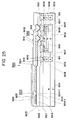
- Fig. 25 is a cross-sectional view of a part of a substrate for a recording head according to the aforementioned constitution.
- Numeral 901 is a semiconductor supporting member composed of a single-crystal silicon.
- 904 is an epitaxial region of n-type semiconductor and 911 is an ohmic contact region of a n-type semiconductor with high concentration of impurity.
- 905 is a base region of a p-type semiconductor
- 910 is an emitter region of a n-type semiconductor with high concentration of impurity and a bipolar transistor 930 is composed thereby.
- 921 is a heat accumulating layer and 922 is an oxidized silicon layer as an interlaminar insulating layer.
- 923 is a heat-generating resistance layer
- 924 is a wiring electrode of aluminum (Al)
- 925 is an oxidized silicon layer as a protecting layer and a substrate 900 for a recording head is composed of these.
- 920 acts as a heat generating portion.
- a recording head is completed by forming a ceiling plate and liquid paths on the substrate 900.
- the bipolar transistor 930 has a n-p-n transistor structure comprising two high concentration n-type collector regions 911 formed on a n-type collector buried region 902 and the p-type silicon supporting member 901 through the n-type collector buried region 902, two high concentration p-type base region 908 formed inside of the high concentration n-type collector 911 on the n-type collector buried region 902 and through a p-type base buried region 905, and the high concentration n-type emitter region 910 formed between high concentration p-type base regions 908 through the p-type base region 905 and on the n-type collector buried region.
- the bipolar transistor 930 acts as a diode by connecting the high concentration n-type collector region 911 and the high concentration p-type base region 908 with a collector base common electrode 912. Further a p-type isolation buried region 903 as an element separating region, a p-type isolation region 906 and a high concentration p-type isolation region 909 are formed successively.
- a heat generating layer 923 is formed on the p-type silicon supporting member 901 through a n-type epitaxial region 904, a heat accumulating layer 921 and an interlaminar layer 922. By cutting a wiring electrode 924 formed on the heat resistance layer 923, a heat generating member 920 is formed.
- an ink jet recording head substrate 900 having a structure as above mentioned can be manufactured by a process for a semiconductor utilizing a known photolithographic technique.
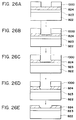
- Figs. 26A to 26E are illustrative views of processes of etching of a material layer 824 for wiring electrode on the heat generating member 920.
- a material layer 824 for a wiring electrode (for example, Al) is formed entirely on the heat generating resistance layer 923, a photoresist for masking 1000 is coated entirely on the material layer 824. After exposing the photoresist 1000 by light with a mask and developing to remove the photoresist corresponding to the portion to be etched of the material layer 824 for the wiring electrode (Fig. 26A).
- the material layer 824 for the electrode is etched by an etching liquid, and at the portion of material layer for the electrode where the photoresist for masking 1000 is removed an electrode for wiring 924 is etched slowly and successively is formed by cutting the material layer for wiring 824 (Figs. 26B to 26D). The remained photoresist for masking 1000 is removed after forming the electrode 924-(Fig. 26E).
- the thickness of the interlaminar layer 922 and the protective film 925 it is necessary to make the thickness of the interlaminar layer 922 and the protective film 925 to be about 1.25 ⁇ m and about 1.0 ⁇ m respectively for well step-covering because the edge part for the connection surface of the electrode and the each wall is stood perpendicularly.
- the too much thickness of about 1.0 ⁇ m as a protective film acts as a heat resistance against the heat conduction of the heat generated at the heat generating portion 920 to an ink, therefore the driving power for the resistance member has to be large and a deterioration of a frequency characteristics caused by the delay of heat conduction may occur.
- the existing of the relatively thick film as insulating film has prohibit from making higher the performance of a conventional heat and saving electricity consumption.
- an interlaminar film 922 and a protective film 925 and etc. have formed by a method such as a normal pressure CVD or PCVD utilizing PSG (phosphoric silicate glass: SiO 2 film containing phosphorus (P); formed from PH 3 + SiH 4 + O 2 ), BPSG (boron phosphoric silicate glass: SiO 2 film containing boron (B) and phosphorus (P); formed from B 2 H 6 + PH 3 + SiH 4 + O 2 ), SiO, SiO 2 , SiON and SiN at 0-450°C. At this temperature range, on a wiring, an electrode, etc.
- PSG phosphoric silicate glass: SiO 2 film containing phosphorus (P); formed from PH 3 + SiH 4 + O 2 ), BPSG (boron phosphoric silicate glass: SiO 2 film containing boron (B) and phosphorus (P); formed from B 2 H 6 + PH 3 + SiH 4 + O 2 ), SiO, SiO 2
- hillrock (often the height and diameter are about 2 ⁇ m) is generated and grown, finally the irregularity of the hillrock may make short-circuit, for example, between the emitter electrode and the wiring electrode or between these wirings and a protective film made of Ta (for example a protective film 926 shown in Fig. 25) and may result a fault of the action and lowers the efficiency of the production.
- EP-A-0378439 discloses a recording head.
- EP-A-0378439 discloses an example in which an NPN transistor is formed on a P type silicon substrate. Furthermore, isolation regions formed by P type isolation buried regions are also disclosed. The process for manufacturing the above-described recording head comprises growing an N type epitaxial region on the P type silicon substrate.
- An embodiment of the present invention provides a method for manufacturing a substrate for a recording head and a recording head employing the substrate, capable of high speed recording and recording with a high resolution.
- the edge faces of said wiring electrodes has an angle of from 30 degree to 75 degree to the normal line of the surface of said electro-thermal converting element.
- an electric current concentration in the edge portion of an electro-thermal converting element can be largely reduced as the electro-thermal converting element contacts with the connecting edge part of the wiring electrode by mutually inclined faces.
- the connected edge part of a wiring electrode of the base member has an inclined surface, an unevenness generated by the forming of the wiring electrode can be formed flatly and it has sufficient step-coverage, to make thin both the inter-layer film and the protecting film.
- the thermal conductive effectivity is improved and as a result, a recording head with low electric energy consumption and good responsibility to frequency can be accomplished at a low cost. And also by relaxation of the electric current concentration a support for a recording head and a recording head can be obtained with elonged life and uniform characteristics.
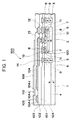
- Fig. 1 is a schematic cross-sectional view of a substrate for a recording head manufactured according to an example included for reference purposes and not an embodiment.
- a substrate 100 as a substrate for a recording head comprises a heat generating portion as an electro-thermal converting element 110 and a bipolar type n-p-n transistor 120 as a driving functional element formed on a p-type silicon supporting member.
- 1 is a p-type silicon supporting member
- 2 is a n-type collector buried region for constructing of a functional element
- 3 is a p-type isolation buried region for separating the functional element
- 4 is a n-type epitaxial region
- 5 is a p-type base region for forming the functional element
- 6 is a p-type isolation buried region for separating the element
- 7 is a n-type collector buried region for constructing an element
- 8 is a high concentration p-type base region for constructing an element
- 9 is a high concentration p-type isolation region
- 10 is a n-type emitter region for constructing an element
- 11 is a high concentration n-type collector region for constructing an element
- 12 is a common electrode for the collector and the base
- 13 is an emitter electrode
- 14 is an isolation electrode.
- n-p-n transistor 120 is formed and the collector portions of 2, 4, 7 and 11 are formed so as to surround entirely the emitter region 10 and the base regions of 5 and 8.
- Each cell is electrically separated by the surrounding p-type isolation buried region 3, p-type isolation region 6 and the high concentration p-type isolation region 9 as the portion for separating elements.
- the n-p-n transistor 120 comprising a n-type buried region 2 and two high concentration n-type collector regions formed on a p-type silicon supporting member a n-type collector buried region 2, the n-type collector buried region 2 and two high concentration p-type base regions 8 formed inside of the high concentration n-type collector region 11 through a p-type base buried region 5, and the n-type collector buried region 2 and the high concentration n-type emitter region 10 formed between a high concentration p-type base region 8 through the p-type base region 5. It acts as a diode by connecting the high concentration n-type collector region 11 and the high concentration p-type base region 8 with a collector base common electrode 12.
- a p-type isolation buried region 3 as an element separating region, a p-type isolation region 6 and a high concentration p-type isolation region are formed in the vicinity of the n-p-n transistor 120 successively.
- a heat generating resistance layer 103 is formed on the p-type silicon supporting member 1 through a n-type epitaxial region 4, a heat accumulating layer 101 and an interlayer film 102 formed integratedly with said heat accumulating layer 101.
- a heat generating portion 110 is constructed by forming two edge parts 104 1 as the connecting surfaces.
- the aforementioned substrate 100 for a recording head is covered entirely on the surface by a heat accumulating layer 101 made of heat oxidized film and etc. and each electrode 12, 13 and 14 from the each element is formed by Al and etc.
- the electrodes 12, 13 and 14 as shown in Fig. 2 and enlarged views (electrode 14, emitter and base are not shown) in Fig. 3 has side surface (wall) inclined angle of theta (at least 30 to up to 75 degree) to the normal line.
- the top surface of the supporting member 100 of this illustrative example comprising the heat accumulating layer 101 thereon formed a collector base common electrode 12, the emitter electrode 13 and the isolation electrode covering the p-type silicon supporting member 1 bearing the above mentioned driving portion (functional element) thereon is covered by an interlayer film 102 composed of silicon oxide film and etc. made by a normal pressure CVD method, PCVD method or sputtering method and etc. Since a step coverage capability is sufficient by the causing of that the portion made of the material such as Al constructing each electrode 12, 13 and 14 have inclined side wall, the interlayer film 102 can be formed thinner than that of a conventional method lest the accumulating effect should be lost.
- an electro-thermal converting element comprising a heat-generating resistance layer 103 of HfB 2 and etc. by sputtering method and a wiring electrode 104 made of Al and etc. by vapor deposition method or sputtering method is provided.
- the material comprising the heat-generating resistance layer include Ta, ZrB 2 , Ti-W, Ni-Cr, Ta-Al, Ta-Si, Ta-Mo, Ta-W, Ta-Cu, Ta-Ni, Ta-Ni-Al, Ta-Mo-Al, Ta-Mo-Ni, Ta-W-Ni, Ta-Si-Al, Ta-W-Al-Ni and etc.
- Fig. 4 is an enlarged schematic cross-sectional view of an electro-thermal converting element and Fig. 5 is an enlarged schematic plan view of an electro-thermal converting element.
- the wiring electrode 104 made of Al and etc. has an edge part 104 1 and side wall 104 2 as a connecting surface inclined at least 30 degree to the normal line.
- a protecting film 105 made of SiO, SiO 2 , SiN, SiON and etc. and a protecting film 106 made of Ta are formed integratedly with the interlayer film 102 by sputtering method or CVD method.
- the substrate 100 has the edge part 104-1 of the wiring electrode 104 being linear tapered and the both side walls 104 (Rf. Fig. 5) which are tapered linearly and the shapes of the collector base common electrode 12, the emitter electrode 13 and the isolation electrode 14 are linear tapered as shown in Fig. 2 and Fig. 3.
- thickness of the first protecting film 105 can be thinned (for example, from 1.0 ⁇ m to 0.6 ⁇ m) compared with the case of the perpendicular shape of the edge part 104-1. Consequently the heat energy generated at the heat generating portion 110 can be conducted effectively and speedily to an ink to be discharged and the through put of an apparatus for forming the protecting film 105 increased by about two times.
- the interlayer film 102 and the protecting film 105 and etc. made of SiO, SiON or SiN and etc. by PCVD method a method where at the initial stage of film formation after the lower layer of the film is formed at low temperature as 150 - 250°C and then the upper layer of the film is grown thereon at 250 - 450°C is conducted.
- the layer formed at lower temperature tends to suppress a grow of a hillock the above mentioned shorting of wiring by a hillock is reduced compared with the case of the film forming one time at 250 - 450°C and the yield of production is remarkably improved.
- edge part connecting surface
- Fig. 7 is a schematic view illustrating the driving manner of the substrate 100 in Fig. 1.
- the collector-base common electrode 12 as shown in Fig. 1 and Fig. 7 corresponds to the anode electrode of the diode and the emitter electrode 13 corresponds to the cathode electrode of the diode.
- V HI collector-base common electrode positive bias potential
- SH1, SH2 collector-base common electrode positive bias potential
- the collector-base common electrode positive bias potential NPN transistor in the cell (SH1, SH2) turns on and the bias current as a collector current and a base current flows from the emitter electrode 13.
- the temperature rising and falling characteristics of the electro-thermal converting element (RH1 and RH2) is improved and subsequently the occurrence of film boiling thereby controlling of the growth and contract of bubble is also improved and consequently the ink discharging is conducted stably.
- the group is selected and simultaneously the electric-thermal converting element RH1 is selected. Then the diode cell SH1 comprising transistor constitution is supplied electric current by a positive bias consequently the electric-thermal converting element RH1 generates heat. This thermal energy gives rise to the change of state of a liquid and makes bubble to discharge liquid through an orifice.
- the P type silicon supporting member 1 is earthed through the isolation region 3, 6 and 9.
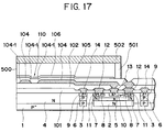
- the substrate 100 thus constructed is able to make a recording head 510 of ink discharging recording system by disposing a sidewall member of liquid path 501 comprising a photosensitive resin and etc. to form liquid path 505 communicated with plural orifices 500 and by disposing a plate member 502 providing an ink supply opening 503.
- ink supplied from the ink supply opening 503 is stored in inner common chamber 504 and then the ink is supplied to each liquid path 505 and at the state by driving the heat generating portion 110 of the substrate 100 the ink is discharged from the orifice 500.
- the results are shown in Table 1.
- the head made of the edge having angle of 30 - 75 degree to the normal line exhibits particularly excellent results on every test.
- the head made of the edge having angle of 5 and 28 degree to the normal line exhibited a good result in the durability test and the one having 80 degree of the angle showed moderately good results on dimensional accuracy of wiring and the variation of the wiring resistance.
- wiring electrode 104 having an edge part 104-1 inclined to a heat generating resistance layer and at the same time having side wall 104-2 inclined along to a longitudinal direction of the wiring electrode 104 can be formed (see Fig. 5).
- a wiring electrode having a connecting edge surface inclined at 30 - 75 degree to the normal line is particularly effective but inclined side wall along to the longitudinal direction is not always necessary.
- the structure having only a connecting edge surface of a wiring electrode inclined and the side wall along the longitudinal direction having near perpendicular inclination as 0 - 30 degree can be achieved.
- the heat generating resistance layer 103a and a material layer made of Al for forming a wiring electrode 104a were formed by repeatedly twice times of the conventional photolithography processing.
- Etching for a wiring electrode 104 can be conducted by the conventional wet etching method or dry etching method as RIE utilizing Cl based gas. By these methods the side wall 104b along the longitudinal direction of wiring electrode 104a being near perpendicular to the normal line can be obtained (Fig. 18).
- a wiring electrode 104a was etched by the same manner as that of forming the emitter electrode, that is, the resist 111 was formed on the wiring electrode 104a so that the resist 111 should not reach to both side surfaces of the wiring electrode 104a when the etching was finished even if the resist 111 was etched back at the etching of wiring electrode 104a.
- the etching of the wiring electrode 104a may be conducted by spraying reciprocally two kinds of alkaline liquid comprising TMAH as the main component and being at different temperature.
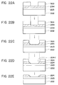
- FIG. 22A to 22E are schematic views of processes of etching a material layer 234 for wiring electrode.
- a material layer 234 made of aluminum was formed entirely on a heat generating resistance layer 223.
- a photoresist for masking (positive type) 300 was coated entirely on the material layer 234. After exposing the photoresist layer 300 with a mask by light and by developing the photoresist 300, the photoresist 300 corresponding to the portion of the material layer for wiring electrode to be etched was removed (Fig. 22A). Then for removing a solvent including in photoresist for masking 300 and for improving the adhesion between the material layer 234 and the photoresist 300, the baking is conducted at 110°C for 90 seconds and the etching of the material layer for wiring electrode 234 was started by multi-wafer system wet etching.
- the etching rate of the material for wiring electrode 234 by the above etchant was about 300 nm/min (3000 ⁇ /min). and the rate of etching (shift of pattern dimension) of the photoresist for masking 300 was about 150 nm/min (1500 ⁇ /min.), on the other hand the rate of the etching of the material layer 234 by the above alkaline solution was 60 nm/min (600 ⁇ /min).
- the taper angle (angle of the surface of the wiring electrode to the normal line) ⁇ of the edge part of the wiring electrode can be controlled desirably by changing the interval of sprayings. In the case of three cycles of alternatively spraying at the time interval as mentioned above, with the alkaline solution and the etchant for wiring electrode, the taper angle of the edge part 224-1 of the wiring electrode 224 was about 55 degree.
- the shape of both side walls (before and backside of the paper) of the electrode 224 was formed as a linear taper as shown in Fig. 5.
- a portion of the oxidized silicon film for forming N-type collector buried region 2 was formed for each cell (each bipolar transistor) was removed by photolithographic technique.
- N-type impurity for example, P, As, etc.
- N-type collector buried region 2 having impurity concentration of at least 1 x 10 18 cm -3 was formed by thermal diffusion method to make the low sheet resistance of 30 ohm/ ⁇ or less at a thickness of 2 to 6 ⁇ m.
- an oxidized silicon film with thickness of about 100 nm (1000 ⁇ ) was formed, and by ion-implanting of P-type impurity (for example B, etc.) a P-type isolation buried region 3 having impurity concentration of at least 1 x 10 15 to 1 x 10 17 cm -3 by thermal diffusion method was formed.
- P-type impurity for example B, etc.
- N-type epitaxial region 4 (impurity concentration of about 1 x 10 13 to about 1 x 10 15 cm -3 ) was grown epitaxially to the thickness of 5 to 20 ⁇ m.
- an oxidized silicon film with a thickness of about 100 nm (1000 ⁇ ) was formed on the surface of the N-type epitaxial region 4, a resist was coated thereon and patterning was conducted and P-type impurity was ion-implanted only at the portion for forming a low concentration P-type base region 5.
- the low concentration P-type base region 5 impurity concentration of at least about 1 x 10 14 to about 1 x 10 17 cm -3
- the oxidized silicon film was entirely removed and further an oxidized silicon film with a thickness of about 800 nm (8000 ⁇ ) was formed, the oxidized silicon film at the portion for forming a P-type isolation buried region 6 was removed, and then BSG film was deposited entirely on the surface by CVD method and then P-type isolation buried region 6 having impurity concentration of about 1 x 10 18 to about 1 x 10 20 cm -3 formed so as to reach to the P-type isolation buried region 3 to a thickness of about 10 ⁇ m by thermal diffusion method.
- P-type isolation buried region 6 can be formed employing BBr 3 as the diffusion source.
- an oxidized silicon film with a thickness of about 800 nm (8000 ⁇ ) was formed.
- a N-type collector region 7 impurity concentration of about 1 x 10 18 to about 1 x 10 20 cm -3 ) was formed to a film thickness about 10 ⁇ m by N-type solid phase diffusion and P ion implantation or by thermal diffusion so that the sheet resistance may have 10 ohm/ ⁇ or less and it may reach to the collector buried region 2.
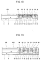
- an oxidized silicon film with a thickness of about 1250 nm (12500 ⁇ ) was formed and after forming a heat accumulating region 101 (see Fig. 13), the oxidized silicon film at the cell region was removed selectively and again an oxidized silicon film with a thickness of about 200 nm (2000 ⁇ ) was formed.
- ion implanting of P-type impurity was conducted into only a portion for forming a high concentration base region 8 and a high concentration isolation region 9.
- the oxidized silicon film at portion for forming N-type emitter region 10 and a high concentration N-type collector region 11 was removed and then thermal oxidized film was formed entirely, after implanting with N-type impurity, N-type emitter region 10 and a high concentration N-type collector region 11 were formed simultaneously by thermal diffusion method.
- the thicknesses of both the N-type emitter region 10 and the high concentration N-type collector region 11 were 1.0 ⁇ m or less and the impurity concentration were about 1 x 10 18 to about 1 x 10 20 cm -3 .
- SiO 2 film as an interlaminar film 102 and also acting as a heat accumulating layer was formed entirely on the surface by sputtering method to have a thickness of about 0.6 to 1.0 ⁇ m.
- the SiO 2 film may be formed by CVD method. There is not limited only SiO 2 but SiO or SiON are available.
- through hole (TH) was formed by opening a part of the interlaminar film 102 corresponding to upper parts of the emitter electrode 13 and the collector base common electrode 12 by photolithography method.
- HfB 2 as a heat generating resistance layer 103 was deposited to thickness of about 100 nm (1000 ⁇ ) on the collector-base electrodes 12 and the emitter electrode 13 and the interlaminar layer (SiO 2 film) through the through hole (TH).
- Al layer on the heat generating resistance layer 103 to a thickness about 500 nm (5000 ⁇ ) as a material of wiring electrode for forming a pair of wiring electrode 104 of the electric-thermal converting element (corresponding to a cathode wiring electrode of a diode) and an anode wiring electrode 109, Al was etched while etching back the photoresist for masking as shown in Fig. 22, so that the shape of the edge part 104-1 with the both side faces of the wiring electrode 104 may have angle of 30 - 70 degree to the normal line.
- a first protecting layer 105 SiO 2 film as a protecting layer for an electro-thermal converting element and an insulating layer for Al wirings was deposited by a spattering method or CVD method, to make a thickness of about 600 nm (6000 ⁇ ), and Ta as a second protecting layer 106 for anticavitation was deposited on upper part of a heat generating portion of an electro-thermal converting element 110 to make a thickness of about 200 nm (2000 ⁇ ).
- the first protecting layer 105 may be made of not SiO 2 but SiON or SiN.
- a step of a producing an ink discharging part having a plurality of openings for discharging an ink formed on the substrate for a recording head (as shown in Fig. 17, that is a step for providing a plurality nozzle walls 501 for forming a discharging opening 500 and a ceiling plate 502) and a step for providing a connector for an ink supply to a ceiling plate 502 (Fig. 18) were added.
- ink jet recording head was examined on block driving of the electro-thermal converting element, on the recording and operation.
- eight semiconductors were connected for one segment and although current of 300 mA was sent (totaly 2.4 A) for each semiconductor diode the other semiconductor operated without malfunction and the sufficient discharging was attained. Since the above recording head has good heat conductive efficiency, the driving power was 80 % of that of the conventional one and the excellent high frequency responsibility was obtained. And also the excellent results on the life time and uniformity were obtained.
- Table 2 one example of evaluation results on the durability of ink jet recording head with edge parts of wiring electrode with various angle ⁇ of the linear taper.
- the wiring electrode 224 was formed by etching the material layer 234.
- the wiring electrode 224 was formed by etching the material layer 234.
- etching rate of aluminum by alkaline solution comprising TMAH as a main component is proportional to the liquid temperature of the alkaline solution (for example, by increasing 10°C it becomes two times). While, the rate of etching back of the photoresist for masking to the alkaline liquid is in inverse proportion to the liquid temperature of the alkaline solution. Therefore, by spraying alternatively two kinds of alkaline solution at the different temperature, while etching back the photoresist for masking 300 for wiring electrode material 234, and by changing the combination of the temperature of the alkaline solution, the angle of the linear taper of the edge part 224-1 of the wiring electrode 224 to be formed can be controlled as desired easily. For example, by giving two cycles of the spraying two kind of the alkaline solution kept at 45°C and 35°C alternatively for 60 sec, the angle of the linear taper of the edge part 224-1 of the wiring electrode 224 was 60 degree.
- both side walls 224-2 of the electrode 224 (Figs. 5 and 22A to 22E) were tapered, but for only reducing the current density of the heat generating portion, the shape of both side walls 224-2 of the electrode 224 may be near perpendicular as shown in Figs. 20 and 21.
- the etching for the material layer for the wiring electrode and the etching for edge part of the wiring electrode to make linear taper were conducted separately. Namely, first by coating a resist entirely on the material layer for wiring electrode and by etching the material layer for wiring electrode utilizing the conventional wet etching method or a dry etching such as RIE employing a C1-based gas, the wiring electrode was formed. In this case the side surface of the wiring electrode was formed as nearly perpendicular shape as the conventional one. A shown in Fig. 19, after coating a photoresist for masking except the portion of the heat generating portion, by etching wiring electrode by manners as shown in Figs. 22A to 22E, the edge part of the wiring electrode having linear tapered shape was obtained as shown in Figs. 20 and 21.
- a material layer 234 composed of aluminum was formed entirely on a heat generating resistance layer 223, a photoresist for masking (positive type) 300 was coated entirely to a thickness of 1.2 ⁇ m on the material layer 234, after exposing the photoresist layer 300 with a mask by light and by developing the photoresist 300, the photoresist for masking corresponding to the portion of the material layer for wiring electrode to be etched was removed (Fig. 22A). Then for removing a solvent including in photoresist for masking 300 and for improving the adhesion between the material layer 234 for wiring electrode and the photoresist 300 for masking, the baking was conducted at 125°C for 225 seconds and the etching of the material layer for wiring electrode 234 was conducted.
- the mixture of phosphoric acid (H 3 PO 4 ), nitric acid (HNO 3 ) and acetic acid (CH 3 COOH) heated as etchant for wiring electrode made of aluminum was known well, but the photoresist for masking can not be etched by this mixture.
- aluminum of the material layer for wiring electrode 234 is amphoteric metal and soluble in an alkaline solution, and a positive type photoresist for masking comprising typically alkaline soluble phenolic resin and naphtoquinone-azide is also soluble in strong alkaline solution.
- an alkaline solution comprising mainly TMAH was used to etch the material layer for wiring electrode.
- the etching-back rate (shift of pattern) of the photoresist for masking 300 was about 1.3 ⁇ m and the taper angle of the edge part of the electrode was 65 degree.
- the both side surfaces (this side and backside of the paper) of the electrode 224 formed will be linear tapered as shown in Fig. 5.
- N-type collector buried region 2 As shown in Fig. 9, after forming an oxidized silicon film of thickness of about 800 nm (8000 ⁇ ) on the surface of a P-type silicon supporting member 1 (impurity concentration of about 1 x 10 12 to 1 x 10 16 cm -3 ), portion of the oxidized silicon film for forming thereon N-type collector buried region 2 for each cell (each bipolar transistor 30) was removed by photolithographic technique. After forming oxidized silicon, by implanting N-type impurity (for example, P, As, etc.), N-type collector buried region 2 having impurity concentration of at least 1 x 10 18 cm -3 was formed by thermal diffusion method to make the low sheet resistance of 30 ohm/ or less to form a thickness of 2 to 6 ⁇ m.
- N-type impurity for example, P, As, etc.
- the portion of the oxidized silicon film for forming P-type isolation buried region 3 was removed and after an oxidized silicon film with a thickness of about 100 nm (1000 ⁇ ) P-type impurity (for example, B, etc.) was ion-implanted to form a P-type isolation buried region 3 having impurity concentration of up to 1 x 10 15 to 1 x 10 17 cm -3 by thermal diffusion method.
- P-type impurity for example, B, etc.
- N-type epitaxial region 4 (impurity concentration of about 1 x 10 13 to 1 x 10 15 cm -3 ) was grown epitaxially to a thickness of 50 to 20 ⁇ m.
- an oxidized silicon film with a thickness of about 100 nm (1000 ⁇ ) was formed on the surface of N-type epitaxial region 4 to coat with a resist and conduct pattern and P-type impurity was ion-implanted only at the portion for forming a low concentration P-type base region 5.
- the low concentration P-type base region 5 impurity concentration of about 5 x 10 14 to 5 x 10 17 cm -3
- thermal diffusion method to a thickness about 5 - 10 ⁇ m.
- the oxidized silicon film was entirely removed and after an oxidized silicon film with a thickness of about 800 nm (8000 ⁇ ) was formed the oxidized silicon film at the portion for forming a P-type isolation buried region 6 was removed, and then BSG film was deposited entirely on the surface by CVD method and then P-type isolation buried region 6 having impurity concentration of about 1 x 10 18 to 1 x 10 20 cm -3 was formed to a thickness of about 10 ⁇ m so that it reached to the P-type isolation buried region 3 by thermal diffusion method.
- P-type isolation buried region 6 can be formed employing BBr 3 as the diffusion source.
- an oxidized silicon film with a thickness of about 800 nm (8000 ⁇ ) was formed, and the oxidized silicon film only at the portion for forming a N-type collector region 7 was removed and a N-type collector region 7 (impurity concentration of about 1 x 10 18 to 1 x 10 20 cm -3 ) was formed to the thickness of about 10 ⁇ m by N-type solid phase diffusion and P ion-implantation or by thermal diffusion so that the sheet resistance has 10 ohm/ or less and it reaches to the collector buried region 2.
- an oxidized silicon film with a thickness of about 1250 nm (12500 ⁇ ) was formed and after forming a heat accumulating layer 101 (see Fig. 13), the oxidized silicon film at the cell region was removed selectively and again an oxidized silicon film with a thickness of about 200 nm (2000 ⁇ ) was formed.
- resist patterning ion-implantation of P-type impurity was conducted into only portion for forming a high concentration base region 8 and a high concentration isolation region 9.
- the oxidized silicon film at the portion for forming N-type emitter region 10 and a high concentration N-type collector region 11 was removed and then thermal oxidized film was formed entirely, after N-type impurity implanting, N-type emitter region 10 and a high concentration N-type collector region 11 were simultaneously by thermal diffusion method.
- the thickness of both the N-type emitter region 10 and the high concentration N-type collector region 11 were 1.0 ⁇ m or less and the impurity concentrations were about 1 x 10 18 to 1 x 10 26 cm -3 .
- SiO 2 film as an interlaminar film 102 and also acting as a heat accumulating layer was formed entirely on the surface by sputtering method to a thickness of about 0.6 to 1.0 ⁇ m.
- the SiO 2 film can be formed by CVD method. There is not limited only SiO 2 but SiO or SiON is available.
- through hole (TH) was formed by opening a part of the interlaminar film 102 corresponding to upper parts of the emitter electrode 13 and the collector base common electrode 12 by photolithography method.
- HfB 2 as a heat generating resistance layer 103 was deposited on the electrodes 12 and 13 through the through hole (TH) corresponding the upper portion of the emitter electrode and the base-collector electrode to a thickness of about 100 nm (1000 ⁇ ).
- An Al layer was deposited to a thickness about 500 nm (5000 ⁇ ) on the heat generating resistance layer 103 as a pair of wiring electrodes 104 of the electric-thermal converting element (corresponding to a cathode wiring electrode for a diode) and an anode wiring electrode 109 of a diode.
- Al was etched while etching back the photoresist for masking as shown in Fig. 22, so that the shape of the edge part 104-1 and the both side faces of the wiring electrode of 104 may have angle of 30 - 70 degree to the normal line.
- a first protecting layer 105 SiO 2 film as a protecting layer for an electro-thermal converting element and an insulating layer for Al wirings was deposited by a sputtering method or CVD method, to a thickness of about 600 nm (6000 ⁇ ) and Ta as a second protecting layer 106 for anti-cavitation was deposited on the upper part of a heat generating portion of an electro-thermal converting element 110 to a thickness of about 200 nm (2000 ⁇ ).
- the first protecting layer 105 may be made of not SiO 2 but SiON or SiN.
- a step of manufacturing an ink discharging part having a plurality of openings for discharging an ink formed on the above substrate for a recording head (as shown in Fig. 17, a step for forming a plurality of nozzle walls 501 for forming a discharging opening 500 a step for disposing a ceiling plate) and a step for disposing a connector for supplying a ink to a ceiling plate 502 (Fig. 18) were added.
- both side walls of the wiring electrode 224 were tapered but for only reducing the current density of the heat generating portion 220, the shape of both side walls of the wiring electrode 224 may be near perpendicular as shown in Figs. 20 and 21.
- the etching for the material layer for wiring electrode and the etching for edge part of wiring electrode to make linear taper were conducted separately. Namely, first by coating with a resist entirely on the material layer for wiring electrode and by etching utilizing the conventional wet etching method or a dry etching by RIE employing a Cl based gas, the wiring electrode was formed. In this case, the side wall of the electrode was formed as nearly perpendicular shape as conventional one. As shown in Fig. 19, after coating with a photoresist for masking except the portion of the heat generating portion, by etching wiring electrode by manners as shown in Figs. 22A to 22E, the edge part of the wiring electrode having linear tapered shape was obtained as shown in Figs. 20 and 21.
- FIGS. 22A to 22E are schematic views showing steps for etching the material layer 234 of wiring electrode.
- a material layer 234 made of aluminum was formed entirely on a heat generating resistance layer 223, a photoresist for masking (positive type) 300 was coated entirely to a thickness of 1.2 ⁇ m on the whole material layer 234. After exposing the photoresist layer 300 with a mask by light, by developing the photoresist 300, the photoresist 300 corresponding to the portion of the material layer for wiring electrode to be etched was removed (Fig. 22A). Then for removing a solvent included in the photoresist for masking 300 and for improving the adhesion between the material layer 234 and the photoresist 300, the baking is conducted at 125°C for 225 seconds and the etching of the material layer for wiring electrode 234 was conducted.
- the mixture of phosphoric acid (H 3 PO 4 ), nitric acid (HNO 3 ) and acetic acid (CH 3 COOH) heated at 45°C as etchant for wiring electrode made of aluminum was well known, but the photoresist for masking can not be etched by this mixture.
- aluminum is amphoteric metal and soluble in an alkaline solution, and a positive type photoresist for masking comprising typically an alkaline soluble phenolic resin and naphtoquinone-azide is also soluble in strong alkaline solution, in this example, an alkaline solution comprising mainly TMAH and kept at a solution temperature of 35°C was used to etch the material layer 234 of wiring electrode.
- both side faces (this side and the backside of the paper) of the electrode 224 formed will be linear tapered as shown in Fig. 5.
- N-type impurity for example, P, As, etc.
- N-type collector buried region 2 having impurity concentration of at least 1 x 10 18 cm -3 was formed by thermal diffusion method to make the low sheet resistance of 30 ohm/ ⁇ or less and to form a thickness of 2 to 6 ⁇ m.
- the portion of the oxidized silicon film for forming P-type isolation buried region 3 was removed and after as oxidized silicon film with thickness of about 100 nm (1000 ⁇ ) was formed and by ion implanting of P-type impurity (for example B, etc.) a P-type isolation buried region 3 having impurity concentration of up to 1 x 10 15 to 1 x 10 17 cm -3 by thermal diffusion method was formed.
- P-type impurity for example B, etc.
- N-type epitaxial region 4 (impurity concentration of about 1 x 10 13 to 1 x 10 15 cm -3 ) was grown epitaxially to a thickness of 5 to 20 ⁇ m.
- an oxidized silicon film with a thickness of about 100 nm (1000 ⁇ ) was formed on the surface of the N-type epitaxial region 4, thereon a resist was coated and pattern forming was conducted, and P-type impurity was ion implanted only at the portion for forming a low concentration P-type base region 5.
- the low concentration P-type base region 5 impurity concentration of about 5 x 10 14 to 1 x 10 17 cm -3
- the oxidized silicon film entirely was removed again and further an oxidized silicon film with a thickness of about 800 nm (8000 ⁇ ) was formed.
- P-type isolation buried region 6 The oxidized silicon film at the portion for forming a P-type isolation buried region 6 was removed, and then BSG film was coated entirely on the surface by CVD method and then P-type isolation buried region 6 having a impurity concentration of about 1 x 10 18 to 1 x 10 20 cm -3 was formed to a thickness of about 10 ⁇ m by thermal diffusion method.
- P-type isolation buried region 6 can be formed employing BBr 3 as the diffusion source.
- an oxidized silicon film with a thickness of about 800 nm (8000 ⁇ ) was formed, and the oxidized silicon film at only the portion for forming a N-type collector region 7 was removed and a N-type collector region 7 (impurity concentration of about 1 x 10 18 to 1 x 10 20 cm -3 ) was formed to a thickness of the film about 10 ⁇ m, by N-type solid phase diffusion and P ion-implantation or by thermal diffusion, so that the sheet resistance has 10 ohm/ ⁇ or less and it reaches to the collector buried region 5.
- an oxidized silicon film with a thickness of about 1250 nm (12500 ⁇ ) was formed, and after forming a heat accumulating portion 101 (see Fig. 13), the oxidized silicon film at the cell region was removed selectively and again an oxidized silicon film with a thickness of about 200 nm (2000 ⁇ ) was formed.
- ion-implantation of P-type impurity was conducted into only portion for forming a high concentration base region 8 and a high concentration isolation region 9.
- the oxidized silicon film portion for forming N-type emitter region 10 and a high concentration N-type collector region 11 was removed, and then thermal oxidized film was formed entirely, after N-type impurity implanting, N-type emitter region 10 and a high concentration N-type collector region 11 were formed simultaneously by thermal diffusion method.
- the thicknesses of both the N-type emitter region 10 and the high concentration N-type collector region 11 were 1.0 ⁇ m or less and the impurity concentrations were about 1 x 10 18 to 1 x 10 20 cm -3 .
- SiO 2 film as an interlaminar film 102 and also acting as a heat accumulating layer was formed entirely on the surface by sputtering method to a thickness of about 0.6 to 1.0 ⁇ m.
- the SiO 2 film can be formed by CVD method. There is not limited only SiO 2 but SiO or SiON is available.
- through hole (TH) was formed by opening a part of the interlaminar film 102 corresponding to upper parts of the emitter electrode 13 and the collector-base common electrode 12 by photolithography method.
- HfB 2 as a heat generating resistance layer 103 was deposited to a thickness of about 100 nm (1000 ⁇ ) on the electrodes 12 and 13 and the interlaminar layer 102 (SiO 2 film) through the through hole (TH).
- a Al layer was deposited to a thickness about 500 nm (5000 ⁇ ) on the heat generating resistance layer 103 as a pair of wiring electrodes 104 of the electric-thermal converting element (corresponding to a cathode wiring electrode for a diode) and an anode wiring electrode 109 for a diode. Then Al was etched while etching back the photoresist for masking as shown in Fig. 22, so that the shape of the edge part 104-1 and the both side faces of the wiring electrode of 104 may have angle of 30 - 70 degree to the normal line.
- a first protecting layer 105 SiO 2 film as a protecting layer for an electro-thermal converting element and an insulating layer for Al wiring was deposited by a sputtering method or CVD method, to make a thickness of about 600 nm (6000 ⁇ ) and Ta as a second protecting layer 106 for anti-cavitation was deposited on the upper part of a heat generating portion of an electro-thermal converting element 110 to make a thickness of about 200 nm (2000 ⁇ ).
- This produced electro-thermal converting element, Ta and SiO 2 film were removed partly to make a part P for bonding.
- the first protecting layer 105 may be made of not SiO 2 but SiON or SiN.
- a step of forming an ink discharging part having a plurality of openings for discharging an ink formed on the substrate for an ink jet recording head (as shown in Fig. 17, steps for forming plural nozzle walls 501 for forming a discharging opening 500 and for disposing a ceiling plate 502) and a step for disposing a connector for supplying an ink in a ceiling plate 502 (Fig. 8) were added.
- ink jet recording head was examined on block driving the electro-thermal converting element, on the recording and operation.
- eight semiconductor diodes were disposed for one segment and current of 300 mA (totaly 2.4 A) was flown in each diode.
- Other semiconductor diodes did not act malfunctionally and the sufficient discharging was obtained.
- the driving power was 80% of that by conventional one and the high frequency responsibility was satisfied. The sufficient characteristics on the life time and uniformity of products were attained.
- the alkaline solution comprising mainly TMAH can be useful for developer for a positive type resist
- an alkaline solution comprising mainly TMAH kept at 30 to 55°C is used for a developer. Therefore, in the example, since the developing step of a photoresist for masking and the etching step of wiring electrode can be conducted successively, the process of manufacturing the substrate is shortened and the improvement of through put can be expected.
- the material layer for wiring electrode 234 was etched while etching back the photoresist for masking 300, and the angle ⁇ of the linear taper of the edge part of the electrode was made to about 70 degree.
- both side walls of the electrode 224 (see Figs. 5 and 22A - 22E) were tapered but for only reducing the current density of the heat generating portion 220, the shape of both side walls of the electrode 224 may be nearly perpendicular as shown in Figs. 20 and 21.
- the etching for the material layer for the wiring electrode and the etching for edge part of the electrode to make linear taper were conducted separately. Namely, first by coating a resist entirely on the material layer for electrode and by etching utilizing the conventional wet etching method or a dry etching such as RIE employing a Cl based gas, the wiring electrode was formed. In this case the side wall of the electrode was formed as nearly perpendicular shape as conventional one. Then as shown in Fig. 19, after coating a photoresist for masking except the portion of the heat generating portion, by etching electrode portion by manners as shown in Figs. 22A to 22E, the edge part of the wiring electrode having linear tapered shape was obtained as shown in Figs. 20 and 21.
- a P-type isolation buried region 3 was formed and then a N-type region 4 was formed by epitaxial growing and thus a low concentration base region 5 and a P-type isolation region 6 were formed.
- a P-type semiconductor layer containing impurity of 5 x 10 14 to 5 x 10 17 cm -3 is formed to a thickness of 5 to 20 ⁇ m, and is used replacing of a region 4, since it can be commonly usable for the low concentration base region 5 and the P-type isolation region 6 and the P-type isolation buried region 3, the steps of formation of these regions (photolithography and heat treatment at high temperature) in the manufacturing can be deleted.
- the head made of the edge having angle of 30 - 75 degree to the normal line exhibits particularly sufficient results on every test term and also on the final judgement.
- the head made of the edge having angle of 5 and 28 degree to the normal line exhibits relatively good results in the durability and the one having 80 degree of the angle showed a moderately good results on the dimensional accuracy of wiring and the scattering of the wiring resistance.
- wiring electrode 104 having an edge part 104-1 inclined to a heat generating resistance layer and at same time having side face inclined along to longitudinal direction of the wiring electrode 104 can be obtainable.
- a wiring electrode having a connecting surface inclined at 30 - 75 degree to the normal line is particularly effective but inclined side wall along to the longitudinal direction is not always necessary.
- the structure having only a connecting surface of a wiring electrode inclined and the side wall along the longitudinal direction having near perpendicular inclination as 0 - 30 degree can be achieved.
- the heat generating resistance layer 103 and a wiring electrode 104 were formed by repeatedly twice times of a conventional photolithography processing.
- Etching for a wiring electrode 104 can be conducted by a conventional wet etching method or dry etching method as RIE utilizing gas such as Cl type (Fig. 18). By these method the side wall 104b along the longitudinal direction of wiring electrode 104a being near perpendicular to the normal line can be obtained.
- resist 111 (a photoresist for masking) was coated except a heat generating resistance layer 103a by a known manner. And the resist 111 was formed on a wiring electrode 104a by a similar manner as forming an emitter electrode and etc. that is, when the etching for the electrode 104a even if the resist 111 was removed backward so that the resist 111 does not reach to the both faces of the electrode 104a and the electrode 104a was etched.
- etching for the wiring electrode 104 may be conducted by spraying alternatively two kinds of alkaline solution containing mainly TMAH at different temperature and thus the structure having inclined edge part 104b at only connecting portion of the heat generating resistance layer 103 can be achieved.
- Fig. 28 is a schematic cross-sectional view of a substrate for ink jet recording head 600a in still another illustrative example provided for reference purposes and not an embodiment.
- the substrate 600a was constituted by covering a P-type silicon substrate 401 bearing a functional element comprising NPN transistor of P-type base regions 405, 408, N-type collector buried region 407, 411 and N-type emitter regions 410 thereon with a heat accumulating layer 601 comprising oxidized film formed a collector base common electrode 412, emitter electrode 413 and isolation electrode 414 thereon and further by forming interlayer film 602 comprising oxidized silicon film etc. by PCVD method or sputtering method on the upper layer.
- each electrode 412, 413 and 414 was made of aluminum and etc. as shown in Figs. 29A and B, the edge part and the side face, that is, all of side faces are formed stepwise (414 not shown in Fig. 29). Since the aluminum forming electrode 412, 413, 414 has steps on the side surface, step coverage of the interlayer film 602 is very much improved and the thickness of the interlayer film 602 can be formed to be thinner than that by a conventional method in the range that the heat accumulating effect should lose.
- Figs. 30A and 30B are enlarged view of the heat generating portion 610.
- edge part and side wall along the longitudinal direction in the wiring 604 composing heat generating portion 610 was formed to be step wise as similar as the above electrode.
- the material for forming heat generating resistance layer 603 includes Ta, ZrB 2 , Ti-W, Ni-Cr, Ta-Al, Ta-Si, Ta-Mo, Ta-W, Ta-Cu, Ta-Ni, Ta-Ni-Al, Ta-Mo-Al, Ta-Mo-Ni, Ta-W-Ni, Ta-Si-Al, Ta-W-Al-Ni and etc.
- a protecting layer 605 made of SiO 2 , SiN or SiON and a protecting layer 606 made of Ta by sputtering method or CVD method as shown in Fig. 28 were provided.
- the edge surface and side wall of the wiring 604 were formed to be stepwise, coverage characteristic of the protecting film 605 is excellent, and the thickness of 1000 nm (10000 ⁇ ) of conventional one can be reduced to 600 nm (6000 ⁇ ), and heat generated at the heat generating portion 610 can be conducted effectively and at high speed.
- the through put of deposition apparatus for a protecting layer was achieved to about two times.
- the concentration of driving current 401A and 401B in the edge part of the heat generating resistance layer 603 as shown in Fig. 31 could be reduced from 8.2 x 10 7 A/cm 2 for a conventional head to 3.2 x 10 7 A/cm 2 and subsequently the durability of the head was improved.
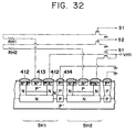
- Fig. 32 is a schematic view illustrating driving method of the heat generating portion 610 of the substrate 600a shown in Fig. 28.
- the collector-base common electrode 412 corresponds to the anode electrode of the diode and the emitter electrode 413 corresponds to the cathode electrode of the diode. Namely, by applying the collector-base common electrode 412 with positive bias potential (V H1 ) NPN transistor in the cell (SH1, SH2) turns on and the bias current as a collector current and a base current flow from the emitter electrode 413.
- V H1 positive bias potential
- SH1, SH2 positive bias potential
- the heat rising and falling characteristics of the electro-thermal converting element (RH1 and RH2) are improved and subsequently the occurrence of film boiling thereby controlling of the growth and contract of bubble is also improved and consequently the ink discharging is conducted stably.
- This fact suggests that the relevancy between the characteristics of transistor and the characteristics of film boiling is strong in a ink jet recording head utilizing thermal energy and since accumulation of minor carrier in a transistor is less, the switching characteristics becomes to faster and the rising characteristics are improved more than those expected. Also since a parastic effect is relatively low and scattering among elements is small, driving current is obtained stably.
- the construction is provided so that by earthing the isolation electrode, 414 flowing of a charge into other neighbor cell and malfunction of the other element should be prevented.
- the driving method of the heat generating portion 610 will be described more in detail below.
- the group is selected and simultaneously the electric-thermal converting element RH1 is selected.
- the functional element cell SH1 comprising transistor constitution is supplied electric current by a positive bias consequently the electric-thermal converting element RH1 generates heat. This thermal energy gives rise the change of state of a liquid and makes bubble to discharge liquid through an orifice.
- the P-type silicon substrate 401 is provided through the isolation regions 403, 406 and 409.
- the isolation regions 403, 406 and 409 of each semiconductor By disposing the isolation regions 403, 406 and 409 of each semiconductor in this manner the wrong action by electric interference between each semiconductor is prevented.
- the substrate 600a constructed in this manner is able to make a recording head comprising liquid path wall member 501 comprising a photosensitive resin and etc. to form liquid path 505 communicated to plural orifices 500 and a lid 502 having an ink supply opening 503.
- ink supplied from the ink supply opening 503 is storaged in an inner common liquid chamber 504 and than the ink is supplied to each liquid path 505 and at the state by driving the heat generating portion 110 the ink is discharged from the orifice 500.
- the step coverage of the interlayer film 602 may be much better with a smaller difference in film thickness between the 1st etching and 2nd etching.
- the etching of Al in the steps of (5) and (8) by conducting the etching of at least two cycles of Al etching - resist removing - Al etching - resist removing - Al etching, the number of the steps formed on the Al edge surface and side wall can be increased as shown in Fig. 43, in which the cross-sectional view of Al wiring edge face as etched four times is shown. By the method the step coverage of the interlayer film 602 can be achieved much better.
- a resist 611 and 611a was coated except a portion corresponding to the heat-generating portion 610 (Fig. 44B), it was immersed in a TMAH aqueous solution by the same manner as described in the manufacturing step (5) of the head 600, by repeating etching and resist removing the region corresponding to the heat-generating portion 610 of the wiring 604 was removed to form the heat-generating portion 610 (Fig. 44C).
- the two connecting faces of the heat-generating portion 610 of the wiring 604 were formed stepwise (Fig. 44D) while the side face is formed to be nearly perpendicular to the surface of the lower heat-generating resistance layer 603.
- This method may be applicable to any electrode of the above functional elements and only connecting face of the electrode can be formed stepwise.
- An ink jet recording apparatus capable of high speed recording with high image quality can be obtained by mounting the thus constituted recording head 510 on the main body of the recording apparatus and by applying a signal from the main body to the recording head 510.
- Fig. 45 is a schematic perspective view illustrating an ink jet recording apparatus 700 to which the present invention is applied.
- the recording head 510 is mounted on a carriage 720 engaged to a screw groove 721 of a lead screw 704 driven through a driving power transferring gear 702 and 703 linked with reciprocally rotation of a driving motor 701 and the head together with the carriage 720 is driven reciprocally along a guide 719 to the direction of arrow "a" and "b” by the driving force of the motor 701.
- 710 is a supporting member for supporting a capping member 711 for covering all over the above recording head 510
- 712 is a suction member for suction of the capping member 711 and plays recovering by suction of the recording head 510 through an opening in the cap 713
- 714 is a cleaning blade
- 715 is a member capable of transferring the blade 714 back and forth carried on a main body supporting board 716.
- the cleaning blade 714 is not necessary to have the shape as shown, but a conventional blade naturally is applicable.
- 717 is a lever for starting the suction for recovery by suction and is transferred depending on the transfer of a cam 718 engaged to carriage 720 and its transfer is controlled by a known manner for transferring such as cratch changing of the driving force from the driving motor 701.
- the print controlling member for applying a signal to the heat-generating portion 110 or controlling the above mechanism mounted on the recording head 510 is built in the main body of the apparatus but not shown in Figure.
- the recording head 510 is driven reciprocally over the entire width of the recording paper P sent to the platen 706 from the recording medium supplying apparatus, and since the recording head 510 is prepared made by the above mentioned method, a high speed recording with high accuracy can be achieved.
- the present invention is particularly effective for a recording head and also a recording apparatus with ink discharging system utilizing thermal energy among ink jet recording systems.
- U.S.Pat. No. 4,723,129 and U.S.Pat. No. 4,740,796 are used preferably.
- This method is applicable to either so-called ondemand type or continuous type, and among them especially the ondemand type is effective, because by exposing an electrothermal converting element which is disposed corresponding to a sheet and liquid path retaining liquid (ink) by at least one drive signal corresponding to a recording information which gives rapid temperature rising over a nuclear boiling, thermal energy is generated in the electrothermal converting element and then film boiling takes place at a heat action surface of the recording head, consequently bubble formation corresponding one to one to the drive signal is occurred in the liquid (ink).
- the liquid (ink) is discharged depending on growing and contraction of the bubble from a discharging opening to form at least one droplet. If the signal is sent as a pulse shape, the growing and contraction is occurred instantaneously and appropriately, consequently a discharging of the liquid (ink) with high responsibility is preferably attained.
- a pulse shaped drive signal which is disclosed in U.S.Pat. No. 4,463,359 and U.S.Pat. No. 4,345,262 is preferably used. And also if taking a condition for a rate of temperature rising up on a heat action surface disclosed in U.S.Pat. No. 4,313,124 the more excellent recording is attained.
- a combination of a discharging opening, a pathway and an electrothermal converting element(a linear liquid pathway or rectangular pathway) disclosed in the above mentioned patent descriptions and a construction of a heat action portion disposed at a flexible domain in disclosed in U.S.Pat. No. 4,558,333 and U.S.Pat. No. 4,459,600 are included in the present invention.
- a construction having a common slit to plural electrothermal converting element as a discharging opening of the electrothermal converting element disclosed in Japanese Laid-Open Patent Application No. 59-123670 and a construction having an opening which is capable of absorbing a pressure wave occurred by thermal energy corresponding to a discharging opening disclosed in Japanese Laid-Open Patent Application No. 59-138462 may include effectively in the present invention.
- the present invention is effective in an interchangeable chip type recording head capable of receiving ink supply from the main body and electrically connecting therewith when it is mounted on the main body and also in the case of cartridge type recording head formed integrally with the recording head itself.
- the recording apparatus is preferably provided with the emission recovery means and other auxiliary means for recording head, since the effects of the recording head of the present invention can be stabilized further.
- Example of such means include capping means, cleaning means, pressurizing or suction means, auxiliary heating means such as an electrothermal converting element, another heating device or a combination thereof and an idle discharging separately from the recording operation are effective for achieving stable recording operation according to the present invention.
- the present invention is not limited to a recording head for recording mode for recording a single main color such as black, but is extremely effective also to the recording head for recording plural different colors or full color by color mixing, wherein the recording head is either integrally constructed or is composed of plural units.
- the recording head of the present invention is applicable, not only to liquid ink, but also to ink which is solid below room temperature but softens or liquifies at room temperature or which softens or lquifies within a temperature control range from 30 to 70°C, which is ordinarily adopted in the ink jet recording.
- ink only needs to be liquidous when the recording signal is given.
- the recording head of the present invention can employ ink liquefied by thermal energy provided corresponding to the recording signal, such as the ink in which the temperature increase by thermal energy is intentionally absorbed by the state change from solid to liquid or the ink which remain solid in the unused state for the purpose of prevention of ink evaporation, or the ink which starts to solidify upon reaching the recording sheet.
- the ink may be supported as solid or liquid in recesses or holes of a porous sheet, as described in the Japanese Patent Laid-Open Application Nos. 54-56847 and 60-71260, and placed in an opposed state to the electrothermal converting element.
- the present invention is most effective when the above mentioned film boiling is induced in the ink as the above mentioned.
Landscapes
- Engineering & Computer Science (AREA)
- Manufacturing & Machinery (AREA)
- Microelectronics & Electronic Packaging (AREA)
- Physics & Mathematics (AREA)
- Condensed Matter Physics & Semiconductors (AREA)
- General Physics & Mathematics (AREA)
- Computer Hardware Design (AREA)
- Power Engineering (AREA)
- Chemical Kinetics & Catalysis (AREA)
- General Chemical & Material Sciences (AREA)
- Chemical & Material Sciences (AREA)
- Particle Formation And Scattering Control In Inkjet Printers (AREA)
- Electronic Switches (AREA)
Claims (13)
- Herstellungsverfahren für eine Trägerschicht bzw. ein Substrat für einen Aufzeichnungskopf mit einer Vielzahl von Elektrizität-Wärme-Umwandlungselementen und Ahsteuerfunktionselementen zum Ansteuern jedes der Elektrizität-Wärne-Umwandlungselemente, wobei das Verfahren das Erzeugen einer p-leitenden Halbleiterschicht durch epitaxiales Aufwachsen auf einem p-leitenden Halbleiter-Tragelement und das Erzeugen der Ansteuerfunktionselemente unter Verwendung der p-leitenden Epitaxialschicht aufweist.
- Herstellungsverfahren für ein Substrat für einen Aufzeichnungskopf, das aufweist:Erzeugen einer p-leitenden Halbleiterschicht durch epitaxiales Aufwachsen auf einem p-leitenden Halbleiter-Tragelement, undVerwenden der p-leitenden Epitaxialschicht beim photolithographischen Ausbilden einer Vielzahl von Elektrizität-Wärme-Umwandlungselementen, einer Vielzahl von Ansteuerfunktionselementen, jeweils zum Ansteuern der Elektrizität-Wärme-Umwandlungselemente, und einer Vielzahl von Verdrahtungselektroden, jeweils zum Verbinden jedes der Ansteuerfunktionselemente, auf der Schicht, wobei die Verdrahtungselektroden durch Ätzen einer Materialschicht für die Verdrahtungselektroden ausgebildet werden, während ein Photoresist zum Maskieren der Materialschicht für die Verdrahtungselektroden bei dem Ätzen entfernt wird.
- Verfahren gemäß Anspruch 2, wobei die Materialschicht für die Verdrahtungselektroden eine Aluminiumschicht ist.
- Verfahren gemäß einem der vorhergehenden Ansprüche, wobei eine elektrische Isolierschicht, die auf den Verdrahtungselementen erzeugt ist, durch ein photolithographisches Verfahren ausgebildet wird, welches das Abscheiden von Material für die elektrische Isolierschicht auf den Verdrahtungselektroden aufweist, während die Temperatur des Tragelements von einer niedrigen Temperatur auf eine hohe Temperatur geändert wird.
- Verfahren gemäß Anspruch 4, wobei das Material für die elektrische Isolierschicht auf den Verdrahtungselektroden abgeschieden wird, während die Temperatur des Tragelements schrittweise von einer niedrigen Temperatur auf eine hohe Temperatur geändert wird.
- Verfahren gemäß Anspruch 4, wobei das Material für die elektrische Isolierschicht auf den Verdrahtungselektroden bei einer Tragelementtemperatur von 150 - 250 °C abgeschieden wird und dann weiterhin bei einer Tragelementtemperatur von 250 - 450 °C der Tragtemperatur darauf abgeschieden wird.
- Verfahren gemäß Anspruch 4, wobei das Material für die elektrische Isolierschicht auf den Verdrahtungselektroden abgeschieden wird, während die Temperatur des Tragelements kontinuierlich von einer niedrigen Temperatur auf eine hohe Temperatur geändert wird.
- Verfahren gemäß Anspruch 4, wobei das Abscheiden der elektrischen Isolierschicht durch ein CVD-Verfahren erfolgt.
- Verfahren gemäß Anspruch 8, wobei das CVD-Verfahren ein Plasma-CVD-Verfahren ist.
- Verfahren gemäß einem der Ansprüche 4 - 9, wobei die elektrische Isolierschicht aus SiO2 besteht.
- Verfahren gemäß einem der Ansprüche 4 - 9, wobei die elektrische Isolierschicht aus SiN besteht.
- Substrat für einen Aufzeichnungskopf, das gemäß dem Verfahren nach einem der vorhergehenden Ansprüche hergestellt ist, wobei die Kantenflächen der Verdrahtungselektroden einen Winkel von 30 Grad bis 75 Grad zu der Normalen der Oberfläche des Elektrizität-Wärme-Umwandlungselements aufweisen.
- Aufzeichnungsvorrichtung mit einem Aufzeichnungskopf, der ein Substrat gemäß Anspruch 12 und eine Einrichtung zum Transportieren eines Aufzeichnungsmediums, auf dem durch die von dem Aufzeichnungskopf ausgestoßene Tinte aufgezeichnet wird, während es in Gegenüberlage zu dem Aufzeichnungskopf angeordnet ist, aufweist.
Priority Applications (1)
| Application Number | Priority Date | Filing Date | Title |
|---|---|---|---|
| EP99200646A EP0925933B1 (de) | 1991-04-20 | 1992-04-16 | Trägerschicht für Aufzeichnungskopf, Aufzeichnungskopf und Herstellungsverfahren dafür |
Applications Claiming Priority (21)
| Application Number | Priority Date | Filing Date | Title |
|---|---|---|---|
| JP11523991A JP3241060B2 (ja) | 1991-04-20 | 1991-04-20 | インクジェット記録ヘッド用基体、インクジェット記録ヘッドおよびインクジェット記録装置 |
| JP11522291 | 1991-04-20 | ||
| JP115239/91 | 1991-04-20 | ||
| JP11524191 | 1991-04-20 | ||
| JP115228/91 | 1991-04-20 | ||
| JP115241/91 | 1991-04-20 | ||
| JP11523991 | 1991-04-20 | ||
| JP11524091 | 1991-04-20 | ||
| JP115238/91 | 1991-04-20 | ||
| JP11522891 | 1991-04-20 | ||
| JP11523891A JP2846501B2 (ja) | 1991-04-20 | 1991-04-20 | 記録ヘッド用基体および記録ヘッドの製造方法 |
| JP11522891A JP2839964B2 (ja) | 1991-04-20 | 1991-04-20 | 記録ヘッド用基体および記録ヘッドの製造方法 |
| JP11524091A JP3046640B2 (ja) | 1991-04-20 | 1991-04-20 | 記録ヘッド用基体の製造方法および記録ヘッドの製造方法 |
| JP11524191A JP3046641B2 (ja) | 1991-04-20 | 1991-04-20 | インクジェット記録ヘッド用基体の製造方法およびインクジェット記録ヘッドの製造方法 |
| JP11522391A JP3173811B2 (ja) | 1991-04-20 | 1991-04-20 | インクジェット記録ヘッド用基体およびインクジェット記録ヘッドの製造方法 |
| JP11523891 | 1991-04-20 | ||
| JP11522391 | 1991-04-20 | ||
| JP11522291A JPH0596731A (ja) | 1991-04-20 | 1991-04-20 | 記録ヘツド用基体および記録ヘツドの製造方法 |
| JP115222/91 | 1991-04-20 | ||
| JP115223/91 | 1991-04-20 | ||
| JP115240/91 | 1991-04-20 |
Related Child Applications (1)
| Application Number | Title | Priority Date | Filing Date |
|---|---|---|---|
| EP99200646A Division EP0925933B1 (de) | 1991-04-20 | 1992-04-16 | Trägerschicht für Aufzeichnungskopf, Aufzeichnungskopf und Herstellungsverfahren dafür |
Publications (3)
| Publication Number | Publication Date |
|---|---|
| EP0518467A2 EP0518467A2 (de) | 1992-12-16 |
| EP0518467A3 EP0518467A3 (en) | 1993-05-12 |
| EP0518467B1 true EP0518467B1 (de) | 1999-10-27 |
Family
ID=27565823
Family Applications (2)
| Application Number | Title | Priority Date | Filing Date |
|---|---|---|---|
| EP92303449A Expired - Lifetime EP0518467B1 (de) | 1991-04-20 | 1992-04-16 | Trägerschicht für Aufzeichnungskopf, Aufzeichnungskopf und Herstellungsverfahren dafür |
| EP99200646A Expired - Lifetime EP0925933B1 (de) | 1991-04-20 | 1992-04-16 | Trägerschicht für Aufzeichnungskopf, Aufzeichnungskopf und Herstellungsverfahren dafür |
Family Applications After (1)
| Application Number | Title | Priority Date | Filing Date |
|---|---|---|---|
| EP99200646A Expired - Lifetime EP0925933B1 (de) | 1991-04-20 | 1992-04-16 | Trägerschicht für Aufzeichnungskopf, Aufzeichnungskopf und Herstellungsverfahren dafür |
Country Status (3)
| Country | Link |
|---|---|
| US (1) | US5376231A (de) |
| EP (2) | EP0518467B1 (de) |
| DE (2) | DE69232872T2 (de) |
Families Citing this family (33)
| Publication number | Priority date | Publication date | Assignee | Title |
|---|---|---|---|---|
| US6168263B1 (en) | 1990-09-21 | 2001-01-02 | Seiko Epson Corporation | Ink jet recording apparatus |
| US6164759A (en) * | 1990-09-21 | 2000-12-26 | Seiko Epson Corporation | Method for producing an electrostatic actuator and an inkjet head using it |
| US6113218A (en) * | 1990-09-21 | 2000-09-05 | Seiko Epson Corporation | Ink-jet recording apparatus and method for producing the head thereof |
| JPH06188108A (ja) * | 1992-12-21 | 1994-07-08 | Canon Inc | 薄膜抵抗器の製造方法、成膜装置用防着板及び成膜装置 |
| JPH07178911A (ja) * | 1993-12-22 | 1995-07-18 | Canon Inc | 記録ヘッド用基体及び記録ヘッド |
| JPH07201864A (ja) * | 1993-12-28 | 1995-08-04 | Fujitsu Ltd | 突起電極形成方法 |
| JP3376128B2 (ja) * | 1994-10-31 | 2003-02-10 | 能美防災株式会社 | 火災感知器用作動試験装置 |
| JP2844051B2 (ja) | 1994-10-31 | 1999-01-06 | セイコーインスツルメンツ株式会社 | サーマルヘッド |
| EP0750990A3 (de) * | 1995-06-28 | 1998-04-01 | Canon Kabushiki Kaisha | Flüssigkeit ausstossender Druckkopf, sein Herstellungsverfahren und Herstellungsverfahren eines Grundkörpers für einen solchen Druckkopf |
| JP3361916B2 (ja) * | 1995-06-28 | 2003-01-07 | シャープ株式会社 | 微小構造の形成方法 |
| US5774148A (en) * | 1995-10-19 | 1998-06-30 | Lexmark International, Inc. | Printhead with field oxide as thermal barrier in chip |
| US6406641B1 (en) | 1997-06-17 | 2002-06-18 | Luxtron Corporation | Liquid etch endpoint detection and process metrology |
| US6267251B1 (en) * | 1997-12-18 | 2001-07-31 | Lexmark International, Inc. | Filter assembly for a print cartridge container for removing contaminants from a fluid |
| US6264309B1 (en) * | 1997-12-18 | 2001-07-24 | Lexmark International, Inc. | Filter formed as part of a heater chip for removing contaminants from a fluid and a method for forming same |
| CN1107592C (zh) * | 2000-01-12 | 2003-05-07 | 威硕科技股份有限公司 | 喷墨头的芯片制造方法 |
| JP2002062665A (ja) * | 2000-08-16 | 2002-02-28 | Koninkl Philips Electronics Nv | 金属膜の製造方法、該金属膜を有する薄膜デバイス、及び該薄膜デバイスを備えた液晶表示装置 |
| US20020158945A1 (en) * | 2001-04-30 | 2002-10-31 | Miller Richard Todd | Heating element of a printhead having resistive layer over conductive layer |
| JP3697196B2 (ja) | 2001-10-22 | 2005-09-21 | キヤノン株式会社 | 記録ヘッド用基体、記録ヘッド及び記録装置 |
| US6933588B1 (en) * | 2002-04-29 | 2005-08-23 | National Semiconductor Corporation | High performance SCR-like BJT ESD protection structure |
| JP4125069B2 (ja) * | 2002-08-13 | 2008-07-23 | キヤノン株式会社 | インクジェット記録ヘッド用基板、インクジェット記録ヘッドおよび該インクジェット記録ヘッドを用いたインクジェット記録装置 |
| US7086718B2 (en) * | 2002-11-23 | 2006-08-08 | Silverbrook Research Pty Ltd | Thermal ink jet printhead with high nozzle areal density |
| US7152958B2 (en) * | 2002-11-23 | 2006-12-26 | Silverbrook Research Pty Ltd | Thermal ink jet with chemical vapor deposited nozzle plate |
| US6719406B1 (en) * | 2002-11-23 | 2004-04-13 | Silverbrook Research Pty Ltd | Ink jet printhead with conformally coated heater |
| US6838351B2 (en) * | 2003-03-31 | 2005-01-04 | Canon Kabushiki Kaisha | Manufacturing method of circuit board, circuit board, and liquid discharging apparatus |
| US7244370B2 (en) * | 2003-08-05 | 2007-07-17 | Canon Kabushiki Kaisha | Method for producing circuit substrate |
| US7837886B2 (en) | 2007-07-26 | 2010-11-23 | Hewlett-Packard Development Company, L.P. | Heating element |
| US7862156B2 (en) * | 2007-07-26 | 2011-01-04 | Hewlett-Packard Development Company, L.P. | Heating element |
| US9237992B2 (en) | 2009-10-27 | 2016-01-19 | The Procter & Gamble Company | Two-step mascara product |
| US9216145B2 (en) | 2009-10-27 | 2015-12-22 | The Procter & Gamble Company | Semi-permanent cosmetic concealer |
| US10034829B2 (en) | 2010-10-27 | 2018-07-31 | Noxell Corporation | Semi-permanent mascara compositions |
| US9004791B2 (en) | 2010-04-30 | 2015-04-14 | The Procter & Gamble Company | Package for multiple personal care compositions |
| US9173824B2 (en) | 2011-05-17 | 2015-11-03 | The Procter & Gamble Company | Mascara and applicator |
| JP2015519954A (ja) | 2012-05-15 | 2015-07-16 | ザ プロクター アンド ギャンブルカンパニー | 睫毛の凝集を定量的に判定する方法 |
Family Cites Families (19)
| Publication number | Priority date | Publication date | Assignee | Title |
|---|---|---|---|---|
| CA1127227A (en) * | 1977-10-03 | 1982-07-06 | Ichiro Endo | Liquid jet recording process and apparatus therefor |
| JPS5936879B2 (ja) * | 1977-10-14 | 1984-09-06 | キヤノン株式会社 | 熱転写記録用媒体 |
| US4330787A (en) * | 1978-10-31 | 1982-05-18 | Canon Kabushiki Kaisha | Liquid jet recording device |
| US4345262A (en) * | 1979-02-19 | 1982-08-17 | Canon Kabushiki Kaisha | Ink jet recording method |
| US4463359A (en) * | 1979-04-02 | 1984-07-31 | Canon Kabushiki Kaisha | Droplet generating method and apparatus thereof |
| US4313124A (en) * | 1979-05-18 | 1982-01-26 | Canon Kabushiki Kaisha | Liquid jet recording process and liquid jet recording head |
| US4429321A (en) | 1980-10-23 | 1984-01-31 | Canon Kabushiki Kaisha | Liquid jet recording device |
| JPS5772867A (en) | 1980-10-23 | 1982-05-07 | Canon Inc | Liquid injecting recording apparatus |
| US4558333A (en) * | 1981-07-09 | 1985-12-10 | Canon Kabushiki Kaisha | Liquid jet recording head |
| JPS59123670A (ja) * | 1982-12-28 | 1984-07-17 | Canon Inc | インクジエツトヘツド |
| JPS59138461A (ja) * | 1983-01-28 | 1984-08-08 | Canon Inc | 液体噴射記録装置 |
| US4425183A (en) * | 1983-08-08 | 1984-01-10 | Ncr Corporation | Metal bevel process for multi-level metal semiconductor applications |
| JPS6071260A (ja) * | 1983-09-28 | 1985-04-23 | Erumu:Kk | 記録装置 |
| US4522681A (en) * | 1984-04-23 | 1985-06-11 | General Electric Company | Method for tapered dry etching |
| JPH0729431B2 (ja) * | 1986-03-04 | 1995-04-05 | キヤノン株式会社 | 液体噴射記録ヘツドの作成方法 |
| US4698128A (en) * | 1986-11-17 | 1987-10-06 | Motorola, Inc. | Sloped contact etch process |
| US5007984A (en) * | 1987-09-28 | 1991-04-16 | Mitsubishi Denki Kabushiki Kaisha | Method for etching chromium film formed on substrate |
| ATE116599T1 (de) * | 1989-01-13 | 1995-01-15 | Canon Kk | Aufzeichnungskopf. |
| US4957592A (en) * | 1989-12-27 | 1990-09-18 | Xerox Corporation | Method of using erodable masks to produce partially etched structures in ODE wafer structures |
-
1992
- 1992-04-16 EP EP92303449A patent/EP0518467B1/de not_active Expired - Lifetime
- 1992-04-16 DE DE69232872T patent/DE69232872T2/de not_active Expired - Fee Related
- 1992-04-16 DE DE69230196T patent/DE69230196T2/de not_active Expired - Fee Related
- 1992-04-16 EP EP99200646A patent/EP0925933B1/de not_active Expired - Lifetime
- 1992-04-20 US US07/871,188 patent/US5376231A/en not_active Expired - Lifetime
Non-Patent Citations (1)
| Title |
|---|
| JOURNAL OF THE ELECTROCHEMICAL SOCIETY vol. 127, no. 12, December 1980, MANCHESTER, NEW HAMPSHIRE, US pages 2687 - 2693 L.K. WHITE 'Bilayer taper etching of field oxides and passivation layers' * |
Also Published As
| Publication number | Publication date |
|---|---|
| DE69232872T2 (de) | 2003-09-18 |
| US5376231A (en) | 1994-12-27 |
| EP0925933A2 (de) | 1999-06-30 |
| DE69232872D1 (de) | 2003-01-23 |
| EP0925933A3 (de) | 1999-09-01 |
| DE69230196T2 (de) | 2000-04-20 |
| EP0518467A3 (en) | 1993-05-12 |
| EP0925933B1 (de) | 2002-12-11 |
| DE69230196D1 (de) | 1999-12-02 |
| EP0518467A2 (de) | 1992-12-16 |
Similar Documents
| Publication | Publication Date | Title |
|---|---|---|
| EP0518467B1 (de) | Trägerschicht für Aufzeichnungskopf, Aufzeichnungskopf und Herstellungsverfahren dafür | |
| US5479197A (en) | Head for recording apparatus | |
| JP3388240B2 (ja) | インクジェットプリントヘッド及びその製造方法 | |
| US7487590B2 (en) | Method for manufacturing monolithic ink-jet printhead having heater disposed between dual ink chambers | |
| US20060290743A1 (en) | Method for manufacturing monolithic ink-jet printhead | |
| US6627467B2 (en) | Fluid ejection device fabrication | |
| US6382775B1 (en) | Liquid ejecting printing head, production method thereof and production method for base body employed for liquid ejecting printing head | |
| US7569404B2 (en) | Ink-jet printhead fabrication | |
| JPH062414B2 (ja) | インクジェットヘッド | |
| US7465404B2 (en) | Ink-jet printhead and method for manufacturing the same | |
| EP0659564B1 (de) | Farbstrahlkopfkassette und Farbstrahlvorrichtung | |
| JP3046640B2 (ja) | 記録ヘッド用基体の製造方法および記録ヘッドの製造方法 | |
| JP3046641B2 (ja) | インクジェット記録ヘッド用基体の製造方法およびインクジェット記録ヘッドの製造方法 | |
| JP2846501B2 (ja) | 記録ヘッド用基体および記録ヘッドの製造方法 | |
| JP3173811B2 (ja) | インクジェット記録ヘッド用基体およびインクジェット記録ヘッドの製造方法 | |
| JPH04320849A (ja) | 記録ヘッド用基体および記録ヘッドの製造方法 | |
| JPH08276597A (ja) | 記録ヘッド用板状基体およびその製造方法ならびに前記記録ヘッド用板状基体を用いた記録ヘッドとこれを搭載する液体噴射記録装置 | |
| JP2003127397A (ja) | 回路基板の製造方法 | |
| JP3241060B2 (ja) | インクジェット記録ヘッド用基体、インクジェット記録ヘッドおよびインクジェット記録装置 | |
| JPH0596731A (ja) | 記録ヘツド用基体および記録ヘツドの製造方法 | |
| KR20040000743A (ko) | 잉크 젯 프린트 헤드 및 이의 제조 방법 |
Legal Events
| Date | Code | Title | Description |
|---|---|---|---|
| PUAI | Public reference made under article 153(3) epc to a published international application that has entered the european phase |
Free format text: ORIGINAL CODE: 0009012 |
|
| AK | Designated contracting states |
Kind code of ref document: A2 Designated state(s): DE FR GB IT NL |
|
| PUAL | Search report despatched |
Free format text: ORIGINAL CODE: 0009013 |
|
| AK | Designated contracting states |
Kind code of ref document: A3 Designated state(s): DE FR GB IT NL |
|
| 17P | Request for examination filed |
Effective date: 19930924 |
|
| 17Q | First examination report despatched |
Effective date: 19950428 |
|
| GRAG | Despatch of communication of intention to grant |
Free format text: ORIGINAL CODE: EPIDOS AGRA |
|
| GRAG | Despatch of communication of intention to grant |
Free format text: ORIGINAL CODE: EPIDOS AGRA |
|
| GRAG | Despatch of communication of intention to grant |
Free format text: ORIGINAL CODE: EPIDOS AGRA |
|
| GRAH | Despatch of communication of intention to grant a patent |
Free format text: ORIGINAL CODE: EPIDOS IGRA |
|
| GRAH | Despatch of communication of intention to grant a patent |
Free format text: ORIGINAL CODE: EPIDOS IGRA |
|
| GRAA | (expected) grant |
Free format text: ORIGINAL CODE: 0009210 |
|
| AK | Designated contracting states |
Kind code of ref document: B1 Designated state(s): DE FR GB IT NL |
|
| REF | Corresponds to: |
Ref document number: 69230196 Country of ref document: DE Date of ref document: 19991202 |
|
| ITF | It: translation for a ep patent filed | ||
| ET | Fr: translation filed | ||
| PLBE | No opposition filed within time limit |
Free format text: ORIGINAL CODE: 0009261 |
|
| STAA | Information on the status of an ep patent application or granted ep patent |
Free format text: STATUS: NO OPPOSITION FILED WITHIN TIME LIMIT |
|
| 26N | No opposition filed | ||
| REG | Reference to a national code |
Ref country code: GB Ref legal event code: IF02 |
|
| AK | Designated contracting states |
Kind code of ref document: A1 Designated state(s): AT BE BG CH CY CZ DE DK EE ES FI FR GB GR HU IE IT LI LU MC NL PT RO SE SI SK TR |
|
| AX | Request for extension of the european patent |
Extension state: AL LT LV MK |
|
| 18W | Application withdrawn |
Effective date: 20050308 |
|
| D17D | Deferred search report published (deleted) | ||
| DA1 | Application published (deleted) | ||
| PGFP | Annual fee paid to national office [announced via postgrant information from national office to epo] |
Ref country code: NL Payment date: 20090427 Year of fee payment: 18 Ref country code: DE Payment date: 20090430 Year of fee payment: 18 Ref country code: IT Payment date: 20090417 Year of fee payment: 18 |
|
| PGFP | Annual fee paid to national office [announced via postgrant information from national office to epo] |
Ref country code: GB Payment date: 20100319 Year of fee payment: 19 |
|
| PGFP | Annual fee paid to national office [announced via postgrant information from national office to epo] |
Ref country code: FR Payment date: 20100430 Year of fee payment: 19 |
|
| REG | Reference to a national code |
Ref country code: NL Ref legal event code: V1 Effective date: 20101101 |
|
| PG25 | Lapsed in a contracting state [announced via postgrant information from national office to epo] |
Ref country code: NL Free format text: LAPSE BECAUSE OF NON-PAYMENT OF DUE FEES Effective date: 20101101 |
|
| PG25 | Lapsed in a contracting state [announced via postgrant information from national office to epo] |
Ref country code: DE Free format text: LAPSE BECAUSE OF NON-PAYMENT OF DUE FEES Effective date: 20101103 |
|
| PG25 | Lapsed in a contracting state [announced via postgrant information from national office to epo] |
Ref country code: IT Free format text: LAPSE BECAUSE OF NON-PAYMENT OF DUE FEES Effective date: 20100416 |
|
| GBPC | Gb: european patent ceased through non-payment of renewal fee |
Effective date: 20110416 |
|
| REG | Reference to a national code |
Ref country code: FR Ref legal event code: ST Effective date: 20111230 |
|
| PG25 | Lapsed in a contracting state [announced via postgrant information from national office to epo] |
Ref country code: FR Free format text: LAPSE BECAUSE OF NON-PAYMENT OF DUE FEES Effective date: 20110502 |
|
| PG25 | Lapsed in a contracting state [announced via postgrant information from national office to epo] |
Ref country code: GB Free format text: LAPSE BECAUSE OF NON-PAYMENT OF DUE FEES Effective date: 20110416 |