EP0513557A2 - Dispositif supraconducteur à effet tunnel - Google Patents
Dispositif supraconducteur à effet tunnel Download PDFInfo
- Publication number
- EP0513557A2 EP0513557A2 EP92106750A EP92106750A EP0513557A2 EP 0513557 A2 EP0513557 A2 EP 0513557A2 EP 92106750 A EP92106750 A EP 92106750A EP 92106750 A EP92106750 A EP 92106750A EP 0513557 A2 EP0513557 A2 EP 0513557A2
- Authority
- EP
- European Patent Office
- Prior art keywords
- superconducting
- layers
- tunnel
- superconductors
- layer
- Prior art date
- Legal status (The legal status is an assumption and is not a legal conclusion. Google has not performed a legal analysis and makes no representation as to the accuracy of the status listed.)
- Granted
Links
Images


Classifications
-
- H—ELECTRICITY
- H10—SEMICONDUCTOR DEVICES; ELECTRIC SOLID-STATE DEVICES NOT OTHERWISE PROVIDED FOR
- H10N—ELECTRIC SOLID-STATE DEVICES NOT OTHERWISE PROVIDED FOR
- H10N60/00—Superconducting devices
- H10N60/10—Junction-based devices
- H10N60/128—Junction-based devices having three or more electrodes, e.g. transistor-like structures
-
- Y—GENERAL TAGGING OF NEW TECHNOLOGICAL DEVELOPMENTS; GENERAL TAGGING OF CROSS-SECTIONAL TECHNOLOGIES SPANNING OVER SEVERAL SECTIONS OF THE IPC; TECHNICAL SUBJECTS COVERED BY FORMER USPC CROSS-REFERENCE ART COLLECTIONS [XRACs] AND DIGESTS
- Y10—TECHNICAL SUBJECTS COVERED BY FORMER USPC
- Y10S—TECHNICAL SUBJECTS COVERED BY FORMER USPC CROSS-REFERENCE ART COLLECTIONS [XRACs] AND DIGESTS
- Y10S505/00—Superconductor technology: apparatus, material, process
- Y10S505/70—High TC, above 30 k, superconducting device, article, or structured stock
- Y10S505/701—Coated or thin film device, i.e. active or passive
- Y10S505/702—Josephson junction present
-
- Y—GENERAL TAGGING OF NEW TECHNOLOGICAL DEVELOPMENTS; GENERAL TAGGING OF CROSS-SECTIONAL TECHNOLOGIES SPANNING OVER SEVERAL SECTIONS OF THE IPC; TECHNICAL SUBJECTS COVERED BY FORMER USPC CROSS-REFERENCE ART COLLECTIONS [XRACs] AND DIGESTS
- Y10—TECHNICAL SUBJECTS COVERED BY FORMER USPC
- Y10S—TECHNICAL SUBJECTS COVERED BY FORMER USPC CROSS-REFERENCE ART COLLECTIONS [XRACs] AND DIGESTS
- Y10S505/00—Superconductor technology: apparatus, material, process
- Y10S505/825—Apparatus per se, device per se, or process of making or operating same
- Y10S505/831—Static information storage system or device
- Y10S505/832—Josephson junction type
-
- Y—GENERAL TAGGING OF NEW TECHNOLOGICAL DEVELOPMENTS; GENERAL TAGGING OF CROSS-SECTIONAL TECHNOLOGIES SPANNING OVER SEVERAL SECTIONS OF THE IPC; TECHNICAL SUBJECTS COVERED BY FORMER USPC CROSS-REFERENCE ART COLLECTIONS [XRACs] AND DIGESTS
- Y10—TECHNICAL SUBJECTS COVERED BY FORMER USPC
- Y10S—TECHNICAL SUBJECTS COVERED BY FORMER USPC CROSS-REFERENCE ART COLLECTIONS [XRACs] AND DIGESTS
- Y10S505/00—Superconductor technology: apparatus, material, process
- Y10S505/825—Apparatus per se, device per se, or process of making or operating same
- Y10S505/848—Radiant energy application
- Y10S505/849—Infrared responsive electric signaling
-
- Y—GENERAL TAGGING OF NEW TECHNOLOGICAL DEVELOPMENTS; GENERAL TAGGING OF CROSS-SECTIONAL TECHNOLOGIES SPANNING OVER SEVERAL SECTIONS OF THE IPC; TECHNICAL SUBJECTS COVERED BY FORMER USPC CROSS-REFERENCE ART COLLECTIONS [XRACs] AND DIGESTS
- Y10—TECHNICAL SUBJECTS COVERED BY FORMER USPC
- Y10S—TECHNICAL SUBJECTS COVERED BY FORMER USPC CROSS-REFERENCE ART COLLECTIONS [XRACs] AND DIGESTS
- Y10S505/00—Superconductor technology: apparatus, material, process
- Y10S505/825—Apparatus per se, device per se, or process of making or operating same
- Y10S505/873—Active solid-state device
- Y10S505/874—Active solid-state device with josephson junction, e.g. squid
-
- Y—GENERAL TAGGING OF NEW TECHNOLOGICAL DEVELOPMENTS; GENERAL TAGGING OF CROSS-SECTIONAL TECHNOLOGIES SPANNING OVER SEVERAL SECTIONS OF THE IPC; TECHNICAL SUBJECTS COVERED BY FORMER USPC CROSS-REFERENCE ART COLLECTIONS [XRACs] AND DIGESTS
- Y10—TECHNICAL SUBJECTS COVERED BY FORMER USPC
- Y10S—TECHNICAL SUBJECTS COVERED BY FORMER USPC CROSS-REFERENCE ART COLLECTIONS [XRACs] AND DIGESTS
- Y10S505/00—Superconductor technology: apparatus, material, process
- Y10S505/825—Apparatus per se, device per se, or process of making or operating same
- Y10S505/917—Mechanically manufacturing superconductor
- Y10S505/922—Making josephson junction device
Definitions
- the invention relates to a superconducting tunnel element.
- SQUID systems are used in medicine and research for the precision measurement of electromagnetic fields.
- Superconducting tunnel elements detect electromagnetic radiation in two different ways: as a broadband detector or as a frequency-selective detector.
- tunnel elements there is a working limit in the direction of small wavelengths, which is predetermined by the energy gap in the excitation spectrum of the superconductor.
- the value of the energy gap can be controlled, for example, with a current loop between the values of the material-specific and temperature-dependent maximum up to zero. Therefore, any spectrum can be set from the short-wave limit ( DE-OS 18 03 953 ).
- the thickness of the barrier determines the type of effect.
- the basic structure of a tunnel element is two or more superconductors separated by a barrier. With barrier thicknesses of more than 1.5 nm to about 3 nm, only single electrons can tunnel.
- EP 329 507 A1 discloses a superconducting element in which a multiplicity of superconducting layers and insulating layers are stacked on one another.
- the layers are only a few atomic layers thick (column 3, line 58) and can be applied using molecular beam epitaxy (column 4, line 20). Electrical connections (eg for control voltages) within the individual layers of the stack are not disclosed.
- JP 2-5580 (A) and JP 2-114576 superconducting optical detectors are known in which several superconducting layers and insulating layers are stacked on top of one another.
- analog / digital converters consist of stacks of superconducting layers of different sizes, that of insulating ones Layers are separated.
- a superconducting element is known, with which a sensor and a transmitter can be realized, in which the frequency range can be set.
- This tunnel element also only detects electromagnetic radiation from a short-wave boundary in the direction of the long-wave spectral region.
- This short-wave limit corresponds energetically to the respective value of the energy gap.
- the value of the energy gap in the tunnel elements can be controlled between the values of the material-specific and temperature-dependent maximum up to zero.
- the object of the invention is to improve such an element that the controllability is improved so that, inter alia, the detection power in the detection mode and the radiation intensity in the transmission mode are multiplied.
- the previous element is improved according to the invention in that the Superconductor integrated, isolated control layers included.
- the number of barriers and superconductors is increased so that there are "stacks".
- the number of superconductors can be set differently from application to application.
- the number of barriers can be set as desired between 3, 4, 5, in particular over 10, and so on up to over 1000.
- a layer sequence of superconducting layers (superconductors) and insulating insulators (barriers) is arranged on a substrate base plate that is compatible with the materials to be used with respect to the lattice constants.
- a superconducting control layer is built into each superconductor, again in isolation.
- a superconductor according to the invention (or tunnel cell, designated SL1 in FIG. 3) thus has the structure: superconducting layer S1 - insulator I - superconducting layer S2 for control purposes - insulator I - superconductor S3.
- Barrier B and the next superconductor SL2 then follow. This is followed by the barrier B2 and then again a superconductor (such a tunnel cell), etc.
- the number of superconductors (tunnel cells) in the tunnel system depends on the manufacturing options and the application goal. It can be big. Each superconductor is separated from the next by a defined barrier. That is why there are many tunnel barriers in this tunnel contact
- the superconducting layers should be as thin as the superconductivity allows. (Eg with high-temperature superconductors in the order of nm).
- the insulators on the flanks of the control superconductors must prevent tunneling and are therefore preferably around 5 nm thick.
- the highest demands are placed on the barriers. They must all be closed (tight) and should have a thickness of 1 to 1.5 nm.
- the layer sequence facing the radiation should meet the condition of the optically thin layer. This means that the superconducting layers must be much smaller than the wavelength of the radiation with which you want to work. The superconducting layers must at least reach the thickness of the material-specific coherence length. This means that the entire stack has a thickness on the order of micrometers. Because of the very thin layers, even the whole stack is just a thin film.
- all superconductors have one connection for the voltage supply and one for the signal current, so that all combinations with the component are possible.
- a current loop In order to control the energy gap for each layer, a current loop must be placed in each superconducting layer. This current loop consists of a superconducting foil that is insulated from the environment. Two opposite flanks of the tunnel stack should preferably remain free of all contacts.
- the voltage is added up with each additional superconductor, with the original energy gap voltage of 2 DELTA being present between each pair of superconductors. If, according to the resulting contact voltage, the tunnel circuit is pretensioned until shortly before the characteristic curve rises, detection is carried out in all barriers, with a slightly larger pretension, in the transmission mode, transmission is carried out in all barriers.
- the tunnel module with several superconductors fulfills the specifications known from DE 40 10 489 A1 .
- the multiple tunnel module according to the invention offers the following significant advantages in a stack:
- the superconducting multiple tunnel element consisting of the new layer sequence of the tunnel cells in the stack, is new in this form.
- the implications of each arrangement are primarily homogeneous fields in each superconducting layer. This enables an individual, uniform control of the energy gap in each superconducting layer and finally any combination of all possible circuits.
- the stacked multiple tunnel element thus becomes a superior instrument.
- Manufacturing and contacting can preferably be carried out using molecular beam epitaxy ( DE 40 10 489 A1 ). This creates the entire sensor cell, including the contact paths to the contacting connections in the molecular beam epitaxy system.
- the contacting is solved by the method of recursive overlap during the layer synthesis.
- the required number of contacts is kept ready on the substrate plate.
- the geometry of the layers can be gradually adapted to the number of contacts required, for example by means of micro-templates.
- the coherence length for high-temperature superconductors is much smaller than for classic superconductors. This fact meets the goal of making the superconducting layers only as thick as necessary. (The minimum extension of a superconductor must be equal to the coherence length, because otherwise superconductivity is not possible).
- FIG. 1 schematically shows a superconducting tunnel element according to the invention, in which twelve superconducting layers SL1 to SL12, which are separated by eleven barriers B1, B2 etc., are applied to a substrate base plate GP . Electrical connections are not yet shown in this figure.
- the counting of the superconducting layers SL1, SL2 etc. starts on the side which is away from the substrate base plate GP .
- the radiation also occurs during sensor operation or the radiation emerges when operated as a radiation source.
- the thicknesses of the barriers BN are 1 to 1.5 nm here, those of the superconducting layers SLN must at least correspond to the coherence length of the superconductor (depending on the material).
- the coherence length is the smallest length over which the Cooper pair density can vary.
- Fig. 2 shows the structure of the two superconductors SL1 and SL2 of Fig. 1 separated from the barrier B in detail.
- the superconductors SL1 and SL2 each contain two superconducting layers S1, S3 and S4, S6 and each have a superconducting control film S2, S5 in their center.
- This control film S2 is isolated from the rest of its superconducting environment (insulating layers I ).
- the control current is present at the control layers S2, S5 , and connections for the working voltage and for the signal current are present on the superconducting layers (here S3 and S4 ).
- the control layer is provided for controlling a homogeneous field in each superconductor SL .
- control layers (control films) S2 , S5 can either be sieve-like or the adjacent superconducting layers S1 , S3 must be short-circuited on the flanks (in our example S1 with S3 and S4 with S6) .
- the individual layers S1 and S3 are spatially separated, but are connected to one another in an electrically conductive manner.
- the insulators I have a thickness> 5 nm.
- 3 and 4 show two possible realizations of the spatial separation, but of the electrical connection of the superconducting individual layers S1 and S3 .
- 3 shows superconducting short-circuit tracks on the flanks of the element, here the two superconductors SL1 and SL2 separated from barrier B are shown.
- the separate superconducting layers S1 and S3 or S4 and S6 are here electrically short-circuited on the flanks by means of superconducting short-circuit bridges.
- the short-circuit bridges are electrically isolated from the control layers S2 and S5 (insulating layers on the flanks).
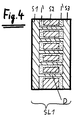
- FIG. 4 shows another embodiment of the superconductor SL1 , in which the electrical connection of the superconducting individual layers S1 and S3 takes place via the penetrations D.
- the control layer S2 is perforated or sieve-like.
- the penetrations D are likewise superconducting, preferably made of the same material as the layers S1 and S3, and are electrically insulated from the control layer S2 (insulations I ' ).
- FIG. 5 shows a circuit diagram of a superconducting multiple tunnel element according to the invention, here for example with twelve superconductors SL1 to SL12 , which are separated from eleven barriers B1 to B11 , on a base plate GP .
- the individual superconducting layers SLN have lateral connections, as shown in FIG. 2, with which they can be activated or deactivated, so that the resulting tunnel voltages can be set as desired (tunnel voltage control TSS ).
- TSS tunnel voltage control
- ELS current loop which enables additional electromagnetic control of the individual energy gaps.
- the working voltage control ASS is also shown.
- the direction of incidence the radiation during sensor operation is indicated by the arrows on the left. When operating as a radiation source, the radiation emerges on the left.
- each SLN superconductor has four connections: two for the working voltage and the signal current I sig and two for the current loop ELS for energy gap control.
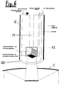
- FIG. 6 shows the diagram of a multispectral transmission and reception system in a Cassegrain mirror C.
- the sensor with control and evaluation electronics designed as an individual sensor or composed of sensor elements is located here in the cryostat K at the focal point of the Cassegrain mirror C.
- the sensor field consists of many individual tunnel elements arranged next to one another, the layers receiving the light (in FIG. 1 SL1 ) each being directed downwards, so that the light to be detected enters the adjacent layers SL1 of the individual tunnel elements via mirror C.
- the cryostat K shows the superinsulation, the vacuum connection, the inflow and the outflow for the liquid nitrogen, the safety valve, the mounting bracket M with control and signal lines, the shielding AS based on superconductivity and the quartz dome QD .
- This miniaturized cryostat K ensures that all superconducting parts remain in the liquid nitrogen at every position in the room. Important parts are safety valves, super insulation and unhindered inflow and outflow.
- the microwave radiation falls through the dome QD onto the sensor.
- the miniaturized cryostat K can thus be made pivotable, as a result of which the sensor can be directed in any direction.
- Macromolecules can be destroyed more easily if they are irradiated specifically with several only those, for example IR frequencies, for which partial molecules have resonances.
- the multispectral sensor and transmission technology is ideal for electronic warfare.
- the signal becomes stronger by many orders of magnitude, namely by the number of superconducting layers N. This applies if all layers of SLN work on exactly the same energy gap.
Applications Claiming Priority (2)
| Application Number | Priority Date | Filing Date | Title |
|---|---|---|---|
| DE4116120 | 1991-05-17 | ||
| DE4116120 | 1991-05-17 |
Publications (3)
| Publication Number | Publication Date |
|---|---|
| EP0513557A2 true EP0513557A2 (fr) | 1992-11-19 |
| EP0513557A3 EP0513557A3 (en) | 1993-02-03 |
| EP0513557B1 EP0513557B1 (fr) | 1998-08-05 |
Family
ID=6431844
Family Applications (1)
| Application Number | Title | Priority Date | Filing Date |
|---|---|---|---|
| EP92106750A Expired - Lifetime EP0513557B1 (fr) | 1991-05-17 | 1992-04-21 | Dispositif supraconducteur à effet tunnel |
Country Status (3)
| Country | Link |
|---|---|
| US (1) | US5347143A (fr) |
| EP (1) | EP0513557B1 (fr) |
| DE (1) | DE59209442D1 (fr) |
Cited By (3)
| Publication number | Priority date | Publication date | Assignee | Title |
|---|---|---|---|---|
| WO1996027214A1 (fr) * | 1995-03-01 | 1996-09-06 | Dornier Gmbh | Elements tunnel supraconducteurs, piles d'elements tunnel et leur utilisation |
| DE19629583C2 (de) * | 1996-07-23 | 2001-04-19 | Oxxel Oxide Electronics Techno | Emitter- und/oder Detektorbauelement für Submillimeterwellen-Strahlung mit einer Vielzahl von Josephson-Kontakten, Verfahren zu seiner Herstellung und Verwendungen des Bauelements |
| US6348699B1 (en) | 1996-07-23 | 2002-02-19 | Oxxel Oxide Electronics Technology Gmbh | Josephson junction array device, and manufacture thereof |
Families Citing this family (7)
| Publication number | Priority date | Publication date | Assignee | Title |
|---|---|---|---|---|
| KR0175359B1 (ko) * | 1995-12-15 | 1999-02-01 | 양승택 | 초전도체-절연체-초전도체 조셉슨 터널 접합구조의 제조방법 |
| US5831278A (en) * | 1996-03-15 | 1998-11-03 | Conductus, Inc. | Three-terminal devices with wide Josephson junctions and asymmetric control lines |
| JP2955931B1 (ja) * | 1998-07-17 | 1999-10-04 | セイコーインスツルメンツ株式会社 | 放射線検出素子 |
| US6384451B1 (en) * | 1999-03-24 | 2002-05-07 | John Caywood | Method and apparatus for injecting charge onto the floating gate of a nonvolatile memory cell |
| JP4747332B2 (ja) * | 2001-06-27 | 2011-08-17 | 独立行政法人 日本原子力研究開発機構 | 超伝導トンネル接合素子を用いた光子及び放射線及び中性子の検出器、及びイメージ検出器 |
| US8519594B2 (en) * | 2010-12-30 | 2013-08-27 | David Mitchell Boie | Hall effect power generator |
| WO2018169579A1 (fr) | 2017-03-13 | 2018-09-20 | Google Llc | Intégration d'éléments de circuit dans un dispositif informatique quantique empilé |
Citations (2)
| Publication number | Priority date | Publication date | Assignee | Title |
|---|---|---|---|---|
| US4334158A (en) * | 1980-06-06 | 1982-06-08 | International Business Machines Corporation | Superconducting switch and amplifier device |
| EP0449559A2 (fr) * | 1990-03-26 | 1991-10-02 | Nippon Steel Corporation | Détection de radiation et détecteur de radiation |
Family Cites Families (10)
| Publication number | Priority date | Publication date | Assignee | Title |
|---|---|---|---|---|
| US3522492A (en) * | 1967-10-23 | 1970-08-04 | Texas Instruments Inc | Superconductive barrier devices |
| US3643237A (en) * | 1969-12-30 | 1972-02-15 | Ibm | Multiple-junction tunnel devices |
| US4837604A (en) * | 1986-04-18 | 1989-06-06 | Hypres, Inc. | Femtosecond three-terminal switch and vertical tunnel junction |
| JPS63248187A (ja) * | 1987-04-03 | 1988-10-14 | Hitachi Ltd | 超伝導デバイス |
| JPH0624260B2 (ja) * | 1987-08-25 | 1994-03-30 | 住友電気工業株式会社 | アナログ/ディジタル変換器 |
| JPH0624259B2 (ja) * | 1987-08-25 | 1994-03-30 | 住友電気工業株式会社 | アナログ/ディジタル変換器 |
| FR2626715B1 (fr) * | 1988-02-02 | 1990-05-18 | Thomson Csf | Dispositif en couches minces de materiau supraconducteur et procede de realisation |
| JPH025580A (ja) * | 1988-06-24 | 1990-01-10 | Canon Inc | 超伝導ビデオ検波素子 |
| JPH02114576A (ja) * | 1988-10-24 | 1990-04-26 | Sharp Corp | 超電導電磁波検出素子 |
| DE4010489A1 (de) * | 1990-03-31 | 1991-10-02 | Dornier Luftfahrt | Supraleitendes element |
-
1992
- 1992-04-21 EP EP92106750A patent/EP0513557B1/fr not_active Expired - Lifetime
- 1992-04-21 DE DE59209442T patent/DE59209442D1/de not_active Expired - Lifetime
-
1993
- 1993-08-09 US US08/103,307 patent/US5347143A/en not_active Expired - Lifetime
Patent Citations (2)
| Publication number | Priority date | Publication date | Assignee | Title |
|---|---|---|---|---|
| US4334158A (en) * | 1980-06-06 | 1982-06-08 | International Business Machines Corporation | Superconducting switch and amplifier device |
| EP0449559A2 (fr) * | 1990-03-26 | 1991-10-02 | Nippon Steel Corporation | Détection de radiation et détecteur de radiation |
Non-Patent Citations (1)
| Title |
|---|
| REVIEW OF SCIENTIFIC INSTRUMENTS Bd. 62, Nr. 1, Januar 1991, NEW YORK, US Seiten 156 - 162 Kurakado M. et al 'Superconductive radiation detector with large sensitive area (series-connected STJ detector)' * |
Cited By (5)
| Publication number | Priority date | Publication date | Assignee | Title |
|---|---|---|---|---|
| WO1996027214A1 (fr) * | 1995-03-01 | 1996-09-06 | Dornier Gmbh | Elements tunnel supraconducteurs, piles d'elements tunnel et leur utilisation |
| DE19607082A1 (de) * | 1995-03-01 | 1996-09-12 | Dornier Gmbh | Supraleitende Tunnelelemente, daraus hergestellte Tunnelstapel sowie deren Verwendung |
| US5955743A (en) * | 1995-03-01 | 1999-09-21 | Schroeder; Hehrwart | Superconductive tunnel elements, tunnel stacks produced therefrom and use thereof |
| DE19629583C2 (de) * | 1996-07-23 | 2001-04-19 | Oxxel Oxide Electronics Techno | Emitter- und/oder Detektorbauelement für Submillimeterwellen-Strahlung mit einer Vielzahl von Josephson-Kontakten, Verfahren zu seiner Herstellung und Verwendungen des Bauelements |
| US6348699B1 (en) | 1996-07-23 | 2002-02-19 | Oxxel Oxide Electronics Technology Gmbh | Josephson junction array device, and manufacture thereof |
Also Published As
| Publication number | Publication date |
|---|---|
| US5347143A (en) | 1994-09-13 |
| DE59209442D1 (de) | 1998-09-10 |
| EP0513557B1 (fr) | 1998-08-05 |
| EP0513557A3 (en) | 1993-02-03 |
Similar Documents
| Publication | Publication Date | Title |
|---|---|---|
| EP1634351B1 (fr) | Antenne quantique supraconductrice | |
| EP1468309B1 (fr) | Detecteur concu pour detecter des faisceaux de particules et procede de fabrication dudit detecteur | |
| EP2443469B1 (fr) | Éléments de résistance électrique et système de mesure pour mesurer des champs magnétiques ou des gradients de champ magnétique variant dans le temps | |
| DE19739477A1 (de) | Pyroelektrische Infrarotsensorvorrichtung | |
| EP0966660A1 (fr) | Capteur a thermopile et thermometre a rayonnement avec capteur a thermopile | |
| EP0513557B1 (fr) | Dispositif supraconducteur à effet tunnel | |
| DE2017067C3 (de) | Pyroelektrischer Detektor | |
| DE3202819C2 (de) | Infrarotdetektor und Verfahren zum Herstellen | |
| DE2816580C2 (de) | Schaltungsanordnung mit einem kapazitiven Strahlungsdetektorelement | |
| DE3425377C2 (de) | Pyroelektrischer Detektor | |
| DE4124048C2 (de) | Supraleitfähiges Bauelement mit einem Josephsonkontakt in einem monokristallinen Hochtemperatursupraleiter und Verfahren zu dessen Herstellung | |
| DE19619585A1 (de) | Schaltbarer planarer Hochfrequenzresonator und Filter | |
| EP0149819B1 (fr) | Senseur de rayonnement et système de mesure comportant un tel senseur exposé au rayonnement ainsi qu'un senseur de référence abrité | |
| DE1803953A1 (de) | Supraleitfaehiges Sperrelement | |
| EP0584866A2 (fr) | Enveloppe de blindage pour magnétomètre à Squid contre des champs électromagnétiques parasites | |
| DE102005011723B3 (de) | Schaltbares Infrarotfilter | |
| DE1489751B2 (de) | Festkoerper infrat festkoerper infrarotbildverstaerker | |
| DE19629583C2 (de) | Emitter- und/oder Detektorbauelement für Submillimeterwellen-Strahlung mit einer Vielzahl von Josephson-Kontakten, Verfahren zu seiner Herstellung und Verwendungen des Bauelements | |
| EP0812479B1 (fr) | Elements tunnel supraconducteurs, piles d'elements tunnel et leur utilisation | |
| DE10041797C2 (de) | Magnetfeldsensitive Dünnfilmsensoreinrichtung mit linearem Sensorelement und Flussantenne | |
| WO1996012305A1 (fr) | Anneau de commutation(squid) a boucle et resonateur supraconducteurs | |
| DE4010489A1 (de) | Supraleitendes element | |
| DE3633286A1 (de) | Matrixsensor zur detektion von infrarotstrahlung | |
| DE2756714A1 (de) | Schaltungsanordnung zur verstaerkung hochfrequenter, elektromagnetischer wellen | |
| DE4219378A1 (de) | Vorrichtung zur räumlich hochauflösenden Erfassung einer flächenhaften Potentialverteilung mittels einer Folienelektrode |
Legal Events
| Date | Code | Title | Description |
|---|---|---|---|
| PUAI | Public reference made under article 153(3) epc to a published international application that has entered the european phase |
Free format text: ORIGINAL CODE: 0009012 |
|
| AK | Designated contracting states |
Kind code of ref document: A2 Designated state(s): DE FR GB IT |
|
| PUAL | Search report despatched |
Free format text: ORIGINAL CODE: 0009013 |
|
| AK | Designated contracting states |
Kind code of ref document: A3 Designated state(s): DE FR GB IT |
|
| 17P | Request for examination filed |
Effective date: 19930730 |
|
| RAP1 | Party data changed (applicant data changed or rights of an application transferred) |
Owner name: DORNIER GMBH |
|
| 17Q | First examination report despatched |
Effective date: 19951215 |
|
| GRAG | Despatch of communication of intention to grant |
Free format text: ORIGINAL CODE: EPIDOS AGRA |
|
| RAP1 | Party data changed (applicant data changed or rights of an application transferred) |
Owner name: SCHROEDER, HEHRWART |
|
| RIN1 | Information on inventor provided before grant (corrected) |
Inventor name: SCHROEDER, HEHRWART |
|
| GRAG | Despatch of communication of intention to grant |
Free format text: ORIGINAL CODE: EPIDOS AGRA |
|
| GRAH | Despatch of communication of intention to grant a patent |
Free format text: ORIGINAL CODE: EPIDOS IGRA |
|
| GRAH | Despatch of communication of intention to grant a patent |
Free format text: ORIGINAL CODE: EPIDOS IGRA |
|
| GRAA | (expected) grant |
Free format text: ORIGINAL CODE: 0009210 |
|
| AK | Designated contracting states |
Kind code of ref document: B1 Designated state(s): DE FR GB IT |
|
| REF | Corresponds to: |
Ref document number: 59209442 Country of ref document: DE Date of ref document: 19980910 |
|
| GBT | Gb: translation of ep patent filed (gb section 77(6)(a)/1977) |
Effective date: 19981106 |
|
| ET | Fr: translation filed | ||
| PLBE | No opposition filed within time limit |
Free format text: ORIGINAL CODE: 0009261 |
|
| STAA | Information on the status of an ep patent application or granted ep patent |
Free format text: STATUS: NO OPPOSITION FILED WITHIN TIME LIMIT |
|
| 26N | No opposition filed | ||
| REG | Reference to a national code |
Ref country code: GB Ref legal event code: IF02 |
|
| PG25 | Lapsed in a contracting state [announced via postgrant information from national office to epo] |
Ref country code: IT Free format text: LAPSE BECAUSE OF NON-PAYMENT OF DUE FEES;WARNING: LAPSES OF ITALIAN PATENTS WITH EFFECTIVE DATE BEFORE 2007 MAY HAVE OCCURRED AT ANY TIME BEFORE 2007. THE CORRECT EFFECTIVE DATE MAY BE DIFFERENT FROM THE ONE RECORDED. Effective date: 20050421 |
|
| REG | Reference to a national code |
Ref country code: GB Ref legal event code: 732E |
|
| PGFP | Annual fee paid to national office [announced via postgrant information from national office to epo] |
Ref country code: DE Payment date: 20100514 Year of fee payment: 19 |
|
| PGFP | Annual fee paid to national office [announced via postgrant information from national office to epo] |
Ref country code: FR Payment date: 20110510 Year of fee payment: 20 |
|
| PGFP | Annual fee paid to national office [announced via postgrant information from national office to epo] |
Ref country code: GB Payment date: 20110421 Year of fee payment: 20 |
|
| PG25 | Lapsed in a contracting state [announced via postgrant information from national office to epo] |
Ref country code: DE Free format text: LAPSE BECAUSE OF NON-PAYMENT OF DUE FEES Effective date: 20111101 |
|
| REG | Reference to a national code |
Ref country code: DE Ref legal event code: R119 Ref document number: 59209442 Country of ref document: DE Effective date: 20111101 |
|
| REG | Reference to a national code |
Ref country code: GB Ref legal event code: PE20 Expiry date: 20120420 |
|
| PG25 | Lapsed in a contracting state [announced via postgrant information from national office to epo] |
Ref country code: GB Free format text: LAPSE BECAUSE OF EXPIRATION OF PROTECTION Effective date: 20120420 |