EP0513557A2 - Superconducting tunneling device - Google Patents
Superconducting tunneling device Download PDFInfo
- Publication number
- EP0513557A2 EP0513557A2 EP92106750A EP92106750A EP0513557A2 EP 0513557 A2 EP0513557 A2 EP 0513557A2 EP 92106750 A EP92106750 A EP 92106750A EP 92106750 A EP92106750 A EP 92106750A EP 0513557 A2 EP0513557 A2 EP 0513557A2
- Authority
- EP
- European Patent Office
- Prior art keywords
- superconducting
- layers
- tunnel
- superconductors
- layer
- Prior art date
- Legal status (The legal status is an assumption and is not a legal conclusion. Google has not performed a legal analysis and makes no representation as to the accuracy of the status listed.)
- Granted
Links
Images


Classifications
-
- H—ELECTRICITY
- H10—SEMICONDUCTOR DEVICES; ELECTRIC SOLID-STATE DEVICES NOT OTHERWISE PROVIDED FOR
- H10N—ELECTRIC SOLID-STATE DEVICES NOT OTHERWISE PROVIDED FOR
- H10N60/00—Superconducting devices
- H10N60/10—Junction-based devices
- H10N60/128—Junction-based devices having three or more electrodes, e.g. transistor-like structures
-
- Y—GENERAL TAGGING OF NEW TECHNOLOGICAL DEVELOPMENTS; GENERAL TAGGING OF CROSS-SECTIONAL TECHNOLOGIES SPANNING OVER SEVERAL SECTIONS OF THE IPC; TECHNICAL SUBJECTS COVERED BY FORMER USPC CROSS-REFERENCE ART COLLECTIONS [XRACs] AND DIGESTS
- Y10—TECHNICAL SUBJECTS COVERED BY FORMER USPC
- Y10S—TECHNICAL SUBJECTS COVERED BY FORMER USPC CROSS-REFERENCE ART COLLECTIONS [XRACs] AND DIGESTS
- Y10S505/00—Superconductor technology: apparatus, material, process
- Y10S505/70—High TC, above 30 k, superconducting device, article, or structured stock
- Y10S505/701—Coated or thin film device, i.e. active or passive
- Y10S505/702—Josephson junction present
-
- Y—GENERAL TAGGING OF NEW TECHNOLOGICAL DEVELOPMENTS; GENERAL TAGGING OF CROSS-SECTIONAL TECHNOLOGIES SPANNING OVER SEVERAL SECTIONS OF THE IPC; TECHNICAL SUBJECTS COVERED BY FORMER USPC CROSS-REFERENCE ART COLLECTIONS [XRACs] AND DIGESTS
- Y10—TECHNICAL SUBJECTS COVERED BY FORMER USPC
- Y10S—TECHNICAL SUBJECTS COVERED BY FORMER USPC CROSS-REFERENCE ART COLLECTIONS [XRACs] AND DIGESTS
- Y10S505/00—Superconductor technology: apparatus, material, process
- Y10S505/825—Apparatus per se, device per se, or process of making or operating same
- Y10S505/831—Static information storage system or device
- Y10S505/832—Josephson junction type
-
- Y—GENERAL TAGGING OF NEW TECHNOLOGICAL DEVELOPMENTS; GENERAL TAGGING OF CROSS-SECTIONAL TECHNOLOGIES SPANNING OVER SEVERAL SECTIONS OF THE IPC; TECHNICAL SUBJECTS COVERED BY FORMER USPC CROSS-REFERENCE ART COLLECTIONS [XRACs] AND DIGESTS
- Y10—TECHNICAL SUBJECTS COVERED BY FORMER USPC
- Y10S—TECHNICAL SUBJECTS COVERED BY FORMER USPC CROSS-REFERENCE ART COLLECTIONS [XRACs] AND DIGESTS
- Y10S505/00—Superconductor technology: apparatus, material, process
- Y10S505/825—Apparatus per se, device per se, or process of making or operating same
- Y10S505/848—Radiant energy application
- Y10S505/849—Infrared responsive electric signaling
-
- Y—GENERAL TAGGING OF NEW TECHNOLOGICAL DEVELOPMENTS; GENERAL TAGGING OF CROSS-SECTIONAL TECHNOLOGIES SPANNING OVER SEVERAL SECTIONS OF THE IPC; TECHNICAL SUBJECTS COVERED BY FORMER USPC CROSS-REFERENCE ART COLLECTIONS [XRACs] AND DIGESTS
- Y10—TECHNICAL SUBJECTS COVERED BY FORMER USPC
- Y10S—TECHNICAL SUBJECTS COVERED BY FORMER USPC CROSS-REFERENCE ART COLLECTIONS [XRACs] AND DIGESTS
- Y10S505/00—Superconductor technology: apparatus, material, process
- Y10S505/825—Apparatus per se, device per se, or process of making or operating same
- Y10S505/873—Active solid-state device
- Y10S505/874—Active solid-state device with josephson junction, e.g. squid
-
- Y—GENERAL TAGGING OF NEW TECHNOLOGICAL DEVELOPMENTS; GENERAL TAGGING OF CROSS-SECTIONAL TECHNOLOGIES SPANNING OVER SEVERAL SECTIONS OF THE IPC; TECHNICAL SUBJECTS COVERED BY FORMER USPC CROSS-REFERENCE ART COLLECTIONS [XRACs] AND DIGESTS
- Y10—TECHNICAL SUBJECTS COVERED BY FORMER USPC
- Y10S—TECHNICAL SUBJECTS COVERED BY FORMER USPC CROSS-REFERENCE ART COLLECTIONS [XRACs] AND DIGESTS
- Y10S505/00—Superconductor technology: apparatus, material, process
- Y10S505/825—Apparatus per se, device per se, or process of making or operating same
- Y10S505/917—Mechanically manufacturing superconductor
- Y10S505/922—Making josephson junction device
Abstract
Description
Die Erfindung betrifft ein supraleitendes Tunnelelement.The invention relates to a superconducting tunnel element.
Supraleitende Tunnelelemente detektieren elektromagnetische Strahlung im Gegensatz zu konventionellen Detektoren um mehrere Größenordnungen empfindlicher.In contrast to conventional detectors, superconducting tunnel elements detect electromagnetic radiation several orders of magnitude more sensitive.
Als weiterer großer Vorteil ist die extrem kurze Ansprechzeit von supraleitenden Tunnelelementen zu nennen. Sie liegt heute in der Größenordnung von Pico-Sekunden (tmin ≧ e. Φ0/DELTA; wobei e = Elektronenladung, Φ0 = Flußquant und DELTA = Energielücke ist).Another great advantage is the extremely short response time of superconducting tunnel elements. Today it is on the order of pico-seconds (tmin ≧ e. Φ0 / DELTA; where e = electron charge, Φ0 = flux quantum and DELTA = energy gap).
Supraleitende Tunnelelemente für Detektionszwecke gibt es schon seit etwa 25 Jahren. Cooper-Paar-Tunneln und Einzel-Elektron-Tunneln, (auch Quasiteilchen-Tunneln genannt) werden z.B. in der Radio-Astronomie zur Detektion elektromagnetischer Wellen verwendet.Superconducting tunnel elements for detection purposes have been around for about 25 years. Cooper pair tunnels and single electron tunnels (also called quasiparticle tunnels) are e.g. used in radio astronomy for the detection of electromagnetic waves.
SQUID-Systeme werden in der Medizin und Forschung zur Präzisions-Messung elektromagnetischer Felder eingesetzt.SQUID systems are used in medicine and research for the precision measurement of electromagnetic fields.
Supraleitende Tunnelelemente detektieren elektromagnetische Strahlung auf zwei verschiedene Arten: als Breitband-Detektor oder als frequenzselektiver Detektor.Superconducting tunnel elements detect electromagnetic radiation in two different ways: as a broadband detector or as a frequency-selective detector.
Allgemein gilt für Tunnelelemente, daß eine Arbeits-Grenze in Richtung kleiner Wellenlängen existiert, die durch die Energielücke im Anregungsspektrum des Supraleiters vorgegeben ist.
Die Energielücke ist temperaturabhängig. Sie erreicht bei T = 0 theoretisch ihren größten Wert. Dies bedeutet, daß mit niedrigeren Temperaturen auch die kurzwellige Arbeitsgrenze immer weiter in Richtung kleinerer Wellenlängen verschoben wird.The general rule for tunnel elements is that there is a working limit in the direction of small wavelengths, which is predetermined by the energy gap in the excitation spectrum of the superconductor.
The energy gap is temperature dependent. Theoretically it reaches its greatest value at T = 0. This means that with lower temperatures, the short-wave working limit is shifted further and further towards smaller wavelengths.
Wegen der Abhängigkeit der Ansprechzeit und Schaltzeit von der Energielücke wird auch diese mit abnehmender Temperatur immer geringer. Mit abnehmender Temperatur nimmt darüberhinaus die Rauschtemperatur ab und die Empfindlichkeit zu.Due to the dependence of the response time and switching time on the energy gap, this also decreases with decreasing temperature. As the temperature decreases, the noise temperature also decreases and the sensitivity increases.
Der Wert der Energielücke kann zum Beispiel mit einer Stromschleife zwischen den Werten des materialspezifischen und temperaturabhängigen Maximums bis zu Null gesteuert werden. Deshalb kann ab der kurzwelligen Grenze jedes Spektrum eingestellt werden (DE-OS 18 03 953).The value of the energy gap can be controlled, for example, with a current loop between the values of the material-specific and temperature-dependent maximum up to zero. Therefore, any spectrum can be set from the short-wave limit ( DE-OS 18 03 953 ).
Zwei verschiedene Tunneleffekte können für die Detektion elektromagnetischer Strahlung ausgenutzt werden. Die Dicke der Barriere bestimmt die Art des Effektes. Der prinzipielle Aufbau eines Tunnelelementes sind zwei oder mehrere durch eine Barriere getrennte Supraleiter. Bei Barrierendicken mit mehr als 1,5 nm bis etwa 3 nm können nur noch Einzelelektronen tunneln.Two different tunnel effects can be used for the detection of electromagnetic radiation. The thickness of the barrier determines the type of effect. The basic structure of a tunnel element is two or more superconductors separated by a barrier. With barrier thicknesses of more than 1.5 nm to about 3 nm, only single electrons can tunnel.
Bei Dicken um 1 bis 1,5 nm tunneln Cooper-Paare.Cooper pairs tunnel at thicknesses of 1 to 1.5 nm.
Reihenschaltungen mit mehr als 1000 Josephson-Tunnelelementen wurden gefertigt und untersucht. (J. Niemeyer und J.H. Hinken, Mikrowellen Magazin, Vol. 13 No. 2, 1987, Seite 118).Series connections with more than 1000 Josephson tunnel elements were manufactured and examined. (J. Niemeyer and J.H. Hinken, Microwave Magazine, Vol. 13 No. 2, 1987, page 118).
Aus der EP 329 507 A1 ist ein supraleitendes Element bekannt, bei dem eine Vielzahl von supraleitenden Schichten und isolierenden Schichten aufeinander gestapelt sind. Die Schichten sind nur einige Atomlagen dick (Spalte 3, Zeile 58) und können mit Molekularstrahlepitaxie (Spalte 4, Zeile 20) aufgebracht sein. Elektrische Anschlüsse (z.B. für Steuerspannungen) innerhalb der Einzelschichten des Stapels sind nicht offenbart. EP 329 507 A1 discloses a superconducting element in which a multiplicity of superconducting layers and insulating layers are stacked on one another. The layers are only a few atomic layers thick (column 3, line 58) and can be applied using molecular beam epitaxy (column 4, line 20). Electrical connections (eg for control voltages) within the individual layers of the stack are not disclosed.
Aus der US-Zeitschrift J.App. Phys. 59(11), 1986, Seite 3807 ist ein optischer Detektor mit einer supraleitenden Oxidschicht bekannt.From the US magazine J.App. Phys. 59 (11), 1986, page 3807 an optical detector with a superconducting oxide layer is known.
Aus den Patent Abstract of Japan der JP 63-248187 (A) ist ein Stapel supraleitender und normal leitender dünner Filme bekannt. A stack of superconducting and normally conducting thin films is known from the Patent Abstract of Japan of JP 63-248187 (A) .
Aus den Patent Abstracts of Japan der JP 2-5580 (A) und der JP 2-114576 sind supraleitende optische Detektoren bekannt, bei denen mehrere supraleitende Schichten und isolierenden Schichten aufeinander gestapelt sind.From the Patent Abstracts of Japan of JP 2-5580 (A) and JP 2-114576 superconducting optical detectors are known in which several superconducting layers and insulating layers are stacked on top of one another.
Aus den Patent Abstracts of Japan der JP 62-210708 (A) und der JP 62-210709 (A) sind Analog/Digital-Wandler bekannt, die aus Stapeln von supraleitenden Schichten unterschiedlicher Größe bestehen, die von isolierenden Schichten getrennt sind.From the Patent Abstracts of Japan of JP 62-210708 (A) and JP 62-210709 (A) , analog / digital converters are known which consist of stacks of superconducting layers of different sizes, that of insulating ones Layers are separated.
Aus der US 4,837,604 ist ein supraleitender Schalter mit einem Stapel supraleitender Schichten bekannt, bei denen der Steuerstrom an eine in dem Stapel befindliche Schicht angelegt wird.From US 4,837,604 a superconducting switch with a stack of superconducting layers is known, in which the control current is applied to a layer located in the stack.
Aus der DE 40 10 489 A1 ein supraleitendes Element bekannt, mit dem ein Sensor und ein Sender realisierbar sind, bei denen der Frequenzbereich einstellbar ist. Auch dieses Tunnelelement detektiert elektromagnetische Strahlung erst ab einer kurzwelligen Grenze in Richtung langwelliges Spektralgebiet.From DE 40 10 489 A1 a superconducting element is known, with which a sensor and a transmitter can be realized, in which the frequency range can be set. This tunnel element also only detects electromagnetic radiation from a short-wave boundary in the direction of the long-wave spectral region.
Diese kurzwellige Grenze entspricht dabei energetisch dem jeweiligen Wert der Energielücke. Der Wert der Energielücke kann bei den Tunnelelementen zwischen den Werten des materialspezifischen und temperaturabhängigen Maximums bis zu Null gesteuert werden.This short-wave limit corresponds energetically to the respective value of the energy gap. The value of the energy gap in the tunnel elements can be controlled between the values of the material-specific and temperature-dependent maximum up to zero.
Aufgabe der Erfindung ist es, ein solches Element dahingehend zu verbessern, daß die Steuerbarkeit verbessert wird, so daß unter anderem im Detektionsmodus die Detektionsleistung und im Sendemodus die Strahlungsintensität vervielfacht werden.The object of the invention is to improve such an element that the controllability is improved so that, inter alia, the detection power in the detection mode and the radiation intensity in the transmission mode are multiplied.
Dies wird erfindungsgemäß erreicht von einem Element mit den Merkmalen des Anspruchs 1. Ausführungen der Erfindung sind Gegenstände von Unteransprüchen.This is achieved according to the invention by an element having the features of
Das bisherige Element ist erfindungsgemäß dadurch verbessert, daß die Supraleiter integrierte, isolierte Steuerschichten enthalten. In einer Ausführung der Erfindung ist die Zahl der Barrieren und der Supraleiter erhöht, so daß "Stapel" vorliegen.The previous element is improved according to the invention in that the Superconductor integrated, isolated control layers included. In one embodiment of the invention, the number of barriers and superconductors is increased so that there are "stacks".
Die Anzahl der Supraleiter kann von Anwendung zu Anwendung unterschiedlich eingestellt sein. So ist die Anzahl der Barrieren zwischen 3, 4, 5, insbesondere über 10, und so weiter bis über 1000 beliebig einstellbar.The number of superconductors can be set differently from application to application. The number of barriers can be set as desired between 3, 4, 5, in particular over 10, and so on up to over 1000.
Auf einer Substratgrundplatte, die sich mit den zu verwendenden Materialien bezüglich der Gitterkonstanten verträgt, wird eine Schichtfolge aus supraleitenden Schichten (Supraleiter) und isolierenden Isolatoren (Barrieren) angeordnet. Innerhalb jedes Supraleiters ist - wiederum isoliert - eine supraleitende Steuerschicht eingebaut. Ein erfindungsgemäßer Supraleiter (oder Tunnelzelle, in Fig. 3 als SL1 bezeichnet) hat also den Aufbau: Supraleitende Schicht S1 - Isolator I - supraleitende Schicht S2 zur Steuerung - Isolator I - Supraleiter S3. Es folgt dann die Barriere B und der nächste Supraleiter SL2.
An diesen schließt sich die Barriere B2 an und dann wieder ein Supraleiter (eine solche Tunnelzelle) u.s.w..
Die Anzahl der Supraleiter (Tunnelzellen) im Tunnelsystem ist abhängig von den Fertigungsmöglichkeiten und vom Anwendungs-Ziel. Sie kann groß sein.
Jeder Supraleiter ist von der nächsten durch eine definierte Barriere getrennt.
Deshalb gibt es in diesem Tunnelkontakt viele Tunnel-Barrieren.A layer sequence of superconducting layers (superconductors) and insulating insulators (barriers) is arranged on a substrate base plate that is compatible with the materials to be used with respect to the lattice constants. A superconducting control layer is built into each superconductor, again in isolation. A superconductor according to the invention (or tunnel cell, designated SL1 in FIG. 3) thus has the structure: superconducting layer S1 - insulator I - superconducting layer S2 for control purposes - insulator I - superconductor S3. Barrier B and the next superconductor SL2 then follow.
This is followed by the barrier B2 and then again a superconductor (such a tunnel cell), etc.
The number of superconductors (tunnel cells) in the tunnel system depends on the manufacturing options and the application goal. It can be big.
Each superconductor is separated from the next by a defined barrier.
That is why there are many tunnel barriers in this tunnel contact.
Die supraleitenden Schichten sollen so dünn sein wie es die Funktionsfähigkeit der Supraleitung zuläßt. (Z.B. bei Hochtemperatursupraleitern in der Grössenordnung nm).
Die Isolatoren an den Flanken der Steuer-Supraleiter müssen das Tunneln unterbinden und sind deshalb bevorzugt um 5 nm dick.
An die Barrieren werden die höchsten Anforderungen gestellt. Sie müssen alle geschlossen (dicht) sein und sollen eine Dicke um 1 bis 1,5 nm haben.The superconducting layers should be as thin as the superconductivity allows. (Eg with high-temperature superconductors in the order of nm).
The insulators on the flanks of the control superconductors must prevent tunneling and are therefore preferably around 5 nm thick.
The highest demands are placed on the barriers. They must all be closed (tight) and should have a thickness of 1 to 1.5 nm.
Die der Strahlung zugewandte Schichtenfolge soll die Bedingung der optisch dünnen Schicht erfüllen. Das heißt, die supraleitenden Schichten müssen viel kleiner als die Wellenlänge der Strahlung sein, mit der man arbeiten will. Die supraleitenden Schichten müssen mindestens die Dicke der materialspezifischen Kohärenzlänge erreichen. Das bedeutet, daß der ganze Stapel eine Dicke in der Größenordnung Mikrometer hat. Wegen der sehrdünnen Schichten ist selbst der ganze Stapel nureine dünne Folie.The layer sequence facing the radiation should meet the condition of the optically thin layer. This means that the superconducting layers must be much smaller than the wavelength of the radiation with which you want to work. The superconducting layers must at least reach the thickness of the material-specific coherence length. This means that the entire stack has a thickness on the order of micrometers. Because of the very thin layers, even the whole stack is just a thin film.
Wie bei einem Einzeltunnelelement haben alle Supraleiter je einen Anschluß für die Spannungsversorgung und je einen für den Signalstrom, damit alle Kombinationen mit dem Bauelement möglich werden. Um für jede Schicht die Energielücke steuern zu können, muß in jede supraleitende Schicht eine Stromschleife gelegt werden. Diese Stromschleife besteht aus einer gegenüber der Umgebung isolierten supraleitenden Folie.
Zwei sich gegenüberliegende Flanken des Tunnelstapels sollen bevorzugt von allen Kontaktierungen frei bleiben.As with a single tunnel element, all superconductors have one connection for the voltage supply and one for the signal current, so that all combinations with the component are possible. In order to control the energy gap for each layer, a current loop must be placed in each superconducting layer. This current loop consists of a superconducting foil that is insulated from the environment.
Two opposite flanks of the tunnel stack should preferably remain free of all contacts.
Wie bei einer Reihenschaltung wird die Spannung mit jedem weiteren Supraleiter aufsummiert, wobei zwischen jedem Supraleiterpaar die ursprüngliche Energielückenspannung von 2 DELTA anliegt. Wenn entsprechend der resultierenden Kontaktspannung die Tunnelschaltung bis kurz vor dem Kennlinien-Anstieg vorgespannt wird, wird in allen Barrieren detektiert, bei etwas größerer Vorspannung, im Sendemodus, wird in allen Barrieren gesendet.As with a series connection, the voltage is added up with each additional superconductor, with the original energy gap voltage of 2 DELTA being present between each pair of superconductors. If, according to the resulting contact voltage, the tunnel circuit is pretensioned until shortly before the characteristic curve rises, detection is carried out in all barriers, with a slightly larger pretension, in the transmission mode, transmission is carried out in all barriers.
Der Tunnelbaustein mit mehreren Supraleitern leistet die aus der DE 40 10 489 A1 bekannten Spezifikationen. Gegenüber dem einfachen Tunnelelement bietet der erfindungsgemäße Mehrfachtunnel-Baustein im Stapel unter anderem folgende deutliche Vorteile:
Das supraleitende Mehrfachtunnelelement, bestehend aus der neuen Schichtfolge der Tunnelzellen im Stapel, ist in dieser Form neu. Die sich aus jeder Anordnung ergebenden Folgerungen sind vor allem homogene Felder in jeder supraleitenden Schicht. Dies ermöglicht eine individuelle gleichmässige Steuerung der Energielücke in jeder supraleitenden Schicht und schließlich beliebige Kombinationen aller möglichen Schaltungen. Das gestapelte Mehrfachtunnelelement wird da durch zu einem überlegenden Instrument.The tunnel module with several superconductors fulfills the specifications known from DE 40 10 489 A1 . Compared to the simple tunnel element, the multiple tunnel module according to the invention offers the following significant advantages in a stack:
The superconducting multiple tunnel element, consisting of the new layer sequence of the tunnel cells in the stack, is new in this form. The implications of each arrangement are primarily homogeneous fields in each superconducting layer. This enables an individual, uniform control of the energy gap in each superconducting layer and finally any combination of all possible circuits. The stacked multiple tunnel element thus becomes a superior instrument.
Die wichtigsten Vorteile des neuen Bauelementes gegenüber den bisherigen Tunnelelementen sind im Folgenden:
- Homogene Felder in jeder supraleitenden Schicht
Bisherige Tunnelelemente arbeiten mit einer Steuerschicht an einem Ende des Tunnelelementes. Damit ist eine gleichmäßige Steuerung schon beim einfachen Tunnelelement nicht möglich.
Die neue Schichtfolge arbeitet mit supraleitenden Steuerschichten in jeder supraleitenden Schicht. Die strominduzierten Felder durchfluten jede supraleitende Schicht gleichmäßig von der Mitte her. Diese gleichmäßige, homogene Durchflutung ist Voraussetzung für die volle Steuerfähigkeit des Stapels. - Summierung der Detektorleistung
Wenn die Arbeitsspannung die Bedingung für den Detektionsmodus erfüllt (Arbeitsspannung kleine 2 DELTA), und alle Supraleiter mit gleichen Energielücken gesteuert werden, dann wird sich mit jedem Supraleiter die Detektionsleistung abzüglich der Rauschleistung, (die mit etwa Quadratwurzel zwei pro Schicht wächst) summieren. - Gleichzeitiges Detektieren verschiedener Frequenzen
Wenn N = Anzahl der supraleitenden Schichtpaare ist, dann werden im Detektionsmodus N verschiedene Frequenzen gleichzeitig detektiert, wenn jedes Schichtpaar verschiedene Energielücken hat. Die N verschiedene Frequenzen können individuell eingestellt werden. - Summierung der Strahlungsintensität
Wenn die Arbeitsspannung die Bedingung für den Sendemodus erfüllt (Arbeitsspannung größer 2 DELTA), und alle Schichten mit gleichen Energielücken gesteuert werden, dann wird sich mit jeder Schicht die Strahlungsintensität summieren. - Gleichzeitiges Senden auf verschiedenen Frequenzen
Wenn N = Anzahl der Supraleiterpaare ist, dann werden im Sendemodus n verschiedene Frequenzen gleichzeitig gesendet, wenn jedes Schichtpaar verschiedene Energielücken hat. Die N verschiedene Frequenzen können individuell eingestellt werden. - Kombination beliebiger Frequenzen
Da jede Schicht und jedes Schichtpaar einzeln gesteuert werden kann, gibt es zwischen den Optionen - "alle Schichten gleiche oder alle Schichten verschieden Energielücken" - die Option der beliebigen Kombinationen. Damit können beispielsweise mehrere Schichtpaare für gewünschte ausgesuchte Frequenzen gebündelt werden. - Bau von hochempfindlichen SQUID-Systemen
Für den Einsatz in SQUID-Systemen müssen die einzeln steuerbaren Schichtpaare so geschaltet werden, daß alle Schichten im Stapel bei gleicher Energielücke arbeiten. Dann wird das Ausgangssignal des SQUID-Systems um Größenordnungen stärker. Die Empfindlichkeit wird durch die Stapelanordnung deutlich besser.
- Homogeneous fields in each superconducting layer
Previous tunnel elements work with a control layer at one end of the tunnel element. This is an even control not possible with the simple tunnel element.
The new layer sequence works with superconducting control layers in each superconducting layer. The current-induced fields flow through each superconducting layer evenly from the center. This even, homogeneous flow is a prerequisite for the full controllability of the stack. - Sum of detector power
If the working voltage fulfills the condition for the detection mode (working voltage small 2 DELTA), and all superconductors are controlled with the same energy gaps, then the detection power minus the noise power (which grows with approximately square root two per layer) will add up with each superconductor. - Simultaneous detection of different frequencies
If N = number of superconducting layer pairs, then in the detection mode N different frequencies are detected simultaneously if each layer pair has different energy gaps. The N different frequencies can be set individually. - Summation of the radiation intensity
If the working voltage fulfills the condition for the transmission mode (working voltage greater than 2 DELTA) and all layers are controlled with the same energy gaps, then the radiation intensity will add up with each layer. - Simultaneous transmission on different frequencies
If N = number of superconductor pairs, then n different frequencies are transmitted simultaneously in the transmission mode if each layer pair has different energy gaps. The N different frequencies can be set individually. - Combination of any frequencies
Since each layer and each pair of layers can be controlled individually, there is the option of any combination between the options - "all layers have the same or all layers have different energy gaps". For example, several pairs of layers can be bundled for the desired frequencies selected. - Construction of highly sensitive SQUID systems
For use in SQUID systems, the individually controllable layer pairs must be switched so that all layers in the stack work with the same energy gap. Then the output signal of the SQUID system becomes stronger by orders of magnitude. The sensitivity is significantly improved by the stack arrangement.
Fertigung und Kontaktierung können bevorzugt mit Hilfe der Molekularstrahlepitaxie erfolgen (DE 40 10 489 A1). Dabei entsteht die ganze Sensorzelle einschließlich der Kontaktbahnen zu den Kontaktierungsanschlüssen in der Molekularstrahlepitaxieanlage. Die Kontaktierung wird durch das Verfahren der rekursiven Überlappung während der Schichtensynthese gelöst.Manufacturing and contacting can preferably be carried out using molecular beam epitaxy ( DE 40 10 489 A1 ). This creates the entire sensor cell, including the contact paths to the contacting connections in the molecular beam epitaxy system. The contacting is solved by the method of recursive overlap during the layer synthesis.
Hierzu wird auf der Substratplatte die erforderliche Anzahl von Kontakten bereitgehalten.For this purpose, the required number of contacts is kept ready on the substrate plate.
Da die Bauelementfläche Ausdehnungen in der Größenordnung Millimeter hat, die Kontaktbahnen aber kleiner als Mikrometer werden, kann zum Beispiel durch Mikroschablonen die Geometrie der Schichten stufenweise der Anzahl der erforderlichen Kontakte angepaßt werden.Since the component surface has dimensions of the order of millimeters, but the contact paths become smaller than micrometers, the geometry of the layers can be gradually adapted to the number of contacts required, for example by means of micro-templates.
Bei den Hochtemperatursupraleitern ist die Kohärenzlänge viel kleiner als bei den klassischen Supraleitern. Diese Tatsache kommt dem Ziel entgegen, die supraleitenden Schichten nur so dick wie nötig zu fertigen. (Die Mindestausdehnung eines Supraleiters muß gleich der Kohärenzlänge sein, weil sonst keine Supraleitung möglich ist).The coherence length for high-temperature superconductors is much smaller than for classic superconductors. This fact meets the goal of making the superconducting layers only as thick as necessary. (The minimum extension of a superconductor must be equal to the coherence length, because otherwise superconductivity is not possible).
Die Erfindung wird anhand von sechs Figuren näher erläutert.The invention is explained in more detail with reference to six figures.
Es zeigen:
- Fig. 1
- schematisch ein erfindungsgemäße Tunnelelemente,
- Fig. 2
- ein Detail aus Fig. 1,
- Fig. 3 und 4
- zwei Supraleiter, wie sie in einem erfindungsgemäßen Tunnelelement verwendbar sind,
- Fig. 5
- ein Schaltschema eines erfindungsgemäßen Tunnelelements und
- Fig. 6
- schematisch ein multispektrales Sende- und Empfangssystem in einem Cassegrainspiegel.
- Fig. 1
- schematically a tunnel element according to the invention,
- Fig. 2
- 1 a detail from FIG. 1,
- 3 and 4
- two superconductors as can be used in a tunnel element according to the invention,
- Fig. 5
- a circuit diagram of a tunnel element according to the invention and
- Fig. 6
- schematically a multispectral transmission and reception system in a Cassegrain mirror.
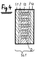
Fig. 1 zeigt schematisch ein erfindungsgemäßes supraleitendes Tunnelelement, bei dem auf einer Substratgrundplatte GP zwölf supraleitende Schichten SL1 bis SL12 aufgebracht sind, die von elf Barrieren B1, B2 usw. getrennt sind. Elektrische Anschlüsse sind in dieser Fig. noch nicht gezeigt.
Die Zählung der supraleitenden Schichten SL1, SL2 usw. beginnt an der Seite, die der Substratgrundplatte GP entfernt liegt. Auf dieser Seite (links) tritt auch bei Sensorbetrieb die Strahlung ein odertritt bei Betrieb als Strahlungsquelle die Strahlung aus. Die Dicken der Barrieren BN liegen hier bei 1 bis 1,5 nm, die der supraleitenden Schichten SLN müssen mindestens der Kohärenzlänge des Supraleiters (materialabhängig) entsprechen. Die Kohärenzlänge ist die kleinste Länge, über die die Cooper-Paardichte variieren kann.1 schematically shows a superconducting tunnel element according to the invention, in which twelve superconducting layers SL1 to SL12, which are separated by eleven barriers B1, B2 etc., are applied to a substrate base plate GP . Electrical connections are not yet shown in this figure.
The counting of the superconducting layers SL1, SL2 etc. starts on the side which is away from the substrate base plate GP . On this page (left), the radiation also occurs during sensor operation or the radiation emerges when operated as a radiation source. The thicknesses of the barriers BN are 1 to 1.5 nm here, those of the superconducting layers SLN must at least correspond to the coherence length of the superconductor (depending on the material). The coherence length is the smallest length over which the Cooper pair density can vary.
Fig. 2 zeigt den Aufbau derzwei von der Barriere B getrennten Supraleiter SL1 und SL2 der Fig. 1 im Detail. Die Supraleiter SL1 und SL2 enthalten je zwei supraleitende Schichten S1, S3 und S4, S6 und haben jeweils in ihrer Mitte je einen supraleitenden Steuerfilm S2, S5. Dieser Steuerfilm S2 ist gegen seine übrige supraleitende Umgebung isoliert (isolierende Schichten I). An den Steuerschichten S2, S5 liegt der Steuerstrom an, an den supraleitenden Schichten (hier S3 und S4) sind Anschlüsse für die Arbeitsspannung und für den Signalstrom vorhanden.
Die Steuerschicht ist zum Steuern eines homogenen Feldes in jedem Supraleiter SL vorhanden. Die Steuerschichten (Steuerfilme) S2, S5 können entweder siebartig sein oder die anliegenden supraleitenden Schichten S1, S3 müssen an den Flanken kurzgeschlossen sein (in unserem Beispiel S1 mit S3 und S4 mit S6). Auf diese beiden Weisen sind die Einzelschichten S1 und S3 räumlich getrennt, aber elektrisch leitfähig miteinander verbunden.
Die Isolatoren I haben eine Dicke > 5 nm.Fig. 2 shows the structure of the two superconductors SL1 and SL2 of Fig. 1 separated from the barrier B in detail. The superconductors SL1 and SL2 each contain two superconducting layers S1, S3 and S4, S6 and each have a superconducting control film S2, S5 in their center. This control film S2 is isolated from the rest of its superconducting environment (insulating layers I ). The control current is present at the control layers S2, S5 , and connections for the working voltage and for the signal current are present on the superconducting layers (here S3 and S4 ).
The control layer is provided for controlling a homogeneous field in each superconductor SL . The control layers (control films) S2 , S5 can either be sieve-like or the adjacent superconducting layers S1 , S3 must be short-circuited on the flanks (in our example S1 with S3 and S4 with S6) . In these two ways, the individual layers S1 and S3 are spatially separated, but are connected to one another in an electrically conductive manner.
The insulators I have a thickness> 5 nm.
Fig. 3 und 4 zeigen zwei mögliche Realisierungen der räumlichen Trennung, aber der elektrischen Verbindung der supraleitenden Einzelschichten S1 und S3.
Fig. 3 zeigt supraleitende Kurzschlußbahnen an den Flanken des Elements, hier gezeigt sind die zwei von der Barriere B getrennten Supraleiter SL1 und SL2. Die voneinander getrennten supraleitenden Schichten S1 und S3 bzw. S4 und S6 sind hier an den Flanken mittels supraleitender Kurzschlußbrücken elektrisch kurzgeschlossen. Die Kurzschlußbrücken sind dabei von den Steuerschichten S2 und S5 elektrisch isoliert (Isolierschichten an den Flanken).3 and 4 show two possible realizations of the spatial separation, but of the electrical connection of the superconducting individual layers S1 and S3 .
3 shows superconducting short-circuit tracks on the flanks of the element, here the two superconductors SL1 and SL2 separated from barrier B are shown. The separate superconducting layers S1 and S3 or S4 and S6 are here electrically short-circuited on the flanks by means of superconducting short-circuit bridges. The short-circuit bridges are electrically isolated from the control layers S2 and S5 (insulating layers on the flanks).
Fig. 4 zeigt eine andere Ausführung des Supraleiters SL1, bei der die elektrische Verbindung der supraleitenden Einzelschichten S1 und S3 über die Durchgriffe D erfolgt. Die Steuerschicht S2 ist dadurch gelocht oder siebartig.
Die Durchgriffe D sind ebenfalls supraleitend, bevorzugt aus dem gleichen Material wie die Schichten S1 und S3 und sind von der Steuerschicht S2 elektrisch isoliert (Isolierungen I').4 shows another embodiment of the superconductor SL1 , in which the electrical connection of the superconducting individual layers S1 and S3 takes place via the penetrations D. The control layer S2 is perforated or sieve-like.
The penetrations D are likewise superconducting, preferably made of the same material as the layers S1 and S3, and are electrically insulated from the control layer S2 (insulations I ' ).
Fig. 5 zeigt ein Schaltschema eines erfindungsgemäßen supraleitenden Mehrfach-Tunnelelements, hier z.B. mit zwölf Supraleitern SL1 bis SL12, die von elf Barrieren B1 bis B11 getrennt sind, auf einer Grundplatte GP. Die einzelnen supraleitenden Schichten SLN haben seitliche Anschlüsse, wie in Fig. 2 gezeigt, mitdenen sie aktiviert oder desaktiviert werden können, so daß die resultierenden Tunnelspannungen beliebig eingestellt werden können (Tunnelspannungssteuerung TSS). Gezeigt ist auch die Stromschleife ELS, mit der eine elektromagnetische Zusatzsteuerung der einzelnen Energielücken ermöglicht ist. Gezeigt ist auch die Arbeitsspannungssteuerung ASS. Die Einfallsrichtung der Strahlung beim Sensorbetrieb ist durch die Pfeile links angedeutet. Beim Betrieb als Strahlungsquelle tritt die Strahlung links aus.5 shows a circuit diagram of a superconducting multiple tunnel element according to the invention, here for example with twelve superconductors SL1 to SL12 , which are separated from eleven barriers B1 to B11 , on a base plate GP . The individual superconducting layers SLN have lateral connections, as shown in FIG. 2, with which they can be activated or deactivated, so that the resulting tunnel voltages can be set as desired (tunnel voltage control TSS ). Also shown is the ELS current loop, which enables additional electromagnetic control of the individual energy gaps. The working voltage control ASS is also shown. The direction of incidence the radiation during sensor operation is indicated by the arrows on the left. When operating as a radiation source, the radiation emerges on the left.
Jeder Supraleiter SLN hat in dieser Ausführung also vier Anschlüsse: Zwei für die Arbeitsspannung und den Signalstrom I sig und zwei für die Stromschleife ELS zur Energielückensteuerung.In this version, each SLN superconductor has four connections: two for the working voltage and the signal current I sig and two for the current loop ELS for energy gap control.
-
Einstellen des Betriebsmodus
Die Arbeitsspannung entscheidet über den Betriebsmodus Detektieren, parametrisch Verstärken und Senden. Dies wird mit einer Präzisions-Spannungsquelle eingestellt. Setting the operating mode
The working voltage decides on the operating mode detection, parametric amplification and transmission. This is set with a precision voltage source. -
Steuerung der Intensität in Stufen und stufenlos
Die Steuerung der Intensität erfolgt am nichtlinearen Teil der Strom-Spannungskennlinie durch Steuerung des Tunnelstromes stufenlos und durch Abschalten der einzelnen Supraleiter SLN in Stufen.
Die Intensität im Sendemodus bzw. die Detektionsleistung kann durch (supraleitende) Schalter (Josphson-Element mit Steuerschicht) zwischen den stillzulegenden supraleitenden Schichten SLN in Stufen gesteuert werden. Dies kann z.B. an den Aussenflächen durch Zu- oder Abschalten geschehen. Diese (supraleitenden) Schalter können über einen Rechner je nach Bedarf aktiviert oder desaktiviert werden.
Die Tunnelschaltung darf in ihrem Innern nicht durch stillgelegte Schichten SLN unterbrochen werden.
Die stufenlose Steuerung der Intensität kann durch Steuerung des Tunnelstromes erfolgen. Bis zum Einsatz supraleitender Bauelemente kann z.B. eine Transistor-Schaltung - in Reihe mit der Präzisions-Spannungsquelle geschaltet - diese Aufgabe erfüllen.
Im linearen der Strom-Spannungskennlinie sollte ein linearer Widerstand die Arbeitsspannung steuern. Im nichtlinearen Kennlinien-Bereich ändert sich die Arbeitsspannung ganz wenig aber der Tunnelstrom steigt hier steil an. Wegen der nichtlinearen Kennlinien-Felder des Transistors läßt sich deshalb damit ein geeignetes Steuerelement zum stufenlosen Steuern des Tunnelstromes realisieren. Control of the intensity in steps and continuously
The intensity is controlled on the non-linear part of the current-voltage characteristic by controlling the tunnel current continuously and by switching off the individual superconductors SLN in stages.
The intensity in the transmission mode or the detection power can be controlled in stages by (superconducting) switches (Josphson element with control layer) between the superconducting layers SLN to be shut down. This can be done, for example, by switching on or off on the outer surfaces. These (superconducting) switches can be activated or deactivated via a computer as required.
The tunnel circuit must not be shut down inside Layers of SLN are interrupted.
The intensity can be steplessly controlled by controlling the tunnel current. A transistor circuit - connected in series with the precision voltage source - can perform this task until superconducting components are used.
A linear resistance should control the working voltage in the linear of the current-voltage characteristic. In the non-linear characteristic range, the working voltage changes very little, but the tunnel current rises steeply here. Because of the non-linear characteristic fields of the transistor, it is therefore possible to implement a suitable control element for stepless control of the tunnel current. -
Elektromagnetische Steuerung der Energielücke
Die Energielücken in den einzelnen supraleitenden Schichten SLN können durch elektromagnetische Felder einheitlich oder individuell von Null bis Maximum gesteuert werden, die von einer supraleitenden Steuerschleife ELS erzeugt werden.
Will man alle Kombinationen des Bauelementes ermöglichen, ist es erforderlich, alle Supraleiter SLN einzeln mit einem speziellen Stromnetz zu versehen. Dieses Stromnetz muß inmitten jeder Schicht so beschaffen sein, daß ein annähernd homogenes Feld auf die supraleitenden Schichten einwirken kann. Zwei mögliche Lösungen sind in den Fig. 3 und 4 gezeigt (Kurzschlußbrücken oder siebartig isolierte supraleitende Schicht inmitten der supraleitenden Einzelschichten SN). Electromagnetic control of the energy gap
The energy gaps in the individual superconducting layers SLN can be controlled uniformly or individually from zero to maximum by electromagnetic fields, which are generated by a superconducting control loop ELS .
If you want to enable all combinations of the component, it is necessary to provide all superconductors SLN individually with a special power network. In the middle of each layer, this power network must be such that an approximately homogeneous field can act on the superconducting layers. 3 and 4 show two possible solutions (short-circuit bridges or sieve-like insulated superconducting layer in the middle of the superconducting individual layers SN ). -
Rechner-Steuerung
Die genannten Funktionen dieses Mehrfachtunnel-Elementes können von einem Rechner kontrolliert und gesteuert werden. Die Überwachung und Steuerung aller genannten Funktionen erfolgt mit Hilfe spezieller Programme. Computer control
The functions of this multiple tunnel element can be controlled and controlled by a computer. The monitoring and control of all the functions mentioned is carried out using special programs.
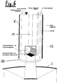
Fig. 6 zeigt das Schema eines multispektralen Sende- und Empfangssystems in einem Cassegrainspiegel C. Der als Einzelsensor ausgebildete oder aus Sensorelementen zusammengesetzte Sensor mit Steuer- und Auswerte-Elektronik befindet sich hier im Kryostaten K im Brennpunkt des Cassegrain-Spiegels C. Das Sensorfeld besteht aus vielen nebeneinander angeordneten Einzeltunnelelementen, wobei jeweils die das Licht aufnehmenden Schichten (in Fig. 1 SL1) nach unten gerichtet sind, so daß das zur detektierende Licht über den Spiegel C in die nebeneinander liegenden Schichten SL1 der einzelnen Tunnelelemente eintritt. Vom Kryostaten K sind die Superisolierung, der Vakuumanschluß, der Zufluß und der Rückfluß für den flüssigen Stickstoff, das Sicherheitsventil, der Montagehalter M mit Steuer- und Signalleitungen, die Abschirmung AS auf Supraleitungsbasis und der Quarzdom QD gezeigt. In diesem miniaturisierten Kryostat K ist sichergestellt, daß alle supraleitenden Teile bei jeder Lage im Raum im flüssigen Stickstoff bleiben.
Wichtige Teile sind Sicherheitsventile, Superisolation und ungehinderter Zuund Abfluß. Die Mikrowellenstrahlung fällt durch den Dom QD auf den Sensor. Der miniaturisierte Kryostat K kann damit schwenkbar ausgebildet werden, wodurch der Sensor in beliebige Richtungen gerichtet werden kann.6 shows the diagram of a multispectral transmission and reception system in a Cassegrain mirror C. The sensor with control and evaluation electronics designed as an individual sensor or composed of sensor elements is located here in the cryostat K at the focal point of the Cassegrain mirror C. The sensor field consists of many individual tunnel elements arranged next to one another, the layers receiving the light (in FIG. 1 SL1 ) each being directed downwards, so that the light to be detected enters the adjacent layers SL1 of the individual tunnel elements via mirror C. The cryostat K shows the superinsulation, the vacuum connection, the inflow and the outflow for the liquid nitrogen, the safety valve, the mounting bracket M with control and signal lines, the shielding AS based on superconductivity and the quartz dome QD . This miniaturized cryostat K ensures that all superconducting parts remain in the liquid nitrogen at every position in the room.
Important parts are safety valves, super insulation and unhindered inflow and outflow. The microwave radiation falls through the dome QD onto the sensor. The miniaturized cryostat K can thus be made pivotable, as a result of which the sensor can be directed in any direction.
Für viele Anwendungen wird diese "flüssige Stickstoffversion" genügen.
Für extreme Anforderungen kann eine Erweiterung mit einem nicht gezeigten Helium-Kryostaten erfolgen. Diese arbeitet dann mit einem zusätzlichen Strahlungsschild aus flüssigem Stickstoff.This "liquid nitrogen version" will suffice for many applications.
For extreme requirements, an extension with a not shown Helium cryostats are made. This then works with an additional radiation shield made of liquid nitrogen.
Diese stichwortartige Auflistung vermittelt einen Eindruck von den interessanten Möglichkeiten, die dieser Baustein mit seiner Flexibilität bietet:
- Analyse von Signalen:
Wegen der sehr hohen Zeitauflösung und hoher Empfindlichkeit ist eine Feinanalyse im ganzen elektromagnetischen Spektrum möglich. - Identifizierung von Signalquellen:
Signalquellen haben charakteristische Muster, die nach Vergleich mit einem Emitterkatalog im Rechner identifiziert werden kann. - Radar-Technik bei freier Wahl des Spektral-Bereiches ab einer kurzwelligen Grenze in Richtung langwelliges Gebiet.
- Passive Zielerkennung und Zielverfolgung ab einer kurzwelligen Grenze in Richtung langwelliges Gebiet.
- Radar für zerstörungsfreie Prüfung.
Wegen der Frequenzabhängigkeit der Absorption durchdringt Radiostrahlung z.B. einige Meter Erdreich, teilweise Staubwolken.
Das konsequente Anwenden des Prinzips der frequenzabhängigen Absorption, gekoppelt mit hoher Empfindlichkeit auf den nahezu wichtigsten Spektralbereich des elektromagnetischen Spektrums führt z.B. zu folgenden weiteren Anwendungen:- passive Ortung von Zielen:
- Auffinden von Verunglückten und Vermißten unter Trümmern, Wasser, Schnee, Fahrzeugen, Schiffen nach Unfällen usw.
- Unterstützung bildgebender Verfahren im Infrarot.
(Für Medizin und Werkstoff-Prüfung)
Kontrastreiche Bilder im IR-Bereich sind wegen des Durchfahrens eines jeweils optimalen Spektrums möglich. - Verschiedene Spektralbereiche machen verschiedene Schichten sichtbar.
- Diagnoseunterstützung in der Medizin mit nichtinvasiven Verfahren.
Die zu analysierenden Moleküle werden zur Rotationsbewegung mit z.B. Mikrowellen angeregt. In vielen Fällen reicht ein Rotations-Übergang aus, da es aufgrund der geringen Linienbreite (≈ 10 kHz) kaum Überlappungen verschiedener Substanzen gibt.
So ist es z.B. möglich, durch gezielte Impuls-Strahlung des supraleitenden Mehrfachtunnel-Bausteins von etwa 1 µs Dauer und einer Frequenz in der Nähe des zu beobachtenden Rotations-Überganges, alle möglichen Substanzen und Verbindungen anzuregen, damit sie dann ihr eigenes Rotations-Spektrum emittieren.
Die zeitlich abklingenden Emissions-Signale würden dann in Abständen von wenigen 10 ns abgetastet und per Rechner verarbeitet werden. (In der Literatur sind z.B. die Rotations-Spektren von mehr als 1500 Verbindungen dokumentiert). - passive Ortung von Zielen:
- Analysis of signals:
Because of the very high time resolution and high sensitivity, a fine analysis in the entire electromagnetic spectrum is possible. - Identification of signal sources:
Signal sources have characteristic patterns that can be identified in the computer after comparison with an emitter catalog. - Radar technology with free choice of the spectral range from a short-wave border in the direction of long-wave area.
- Passive target recognition and target tracking from a short-wave border towards a long-wave area.
- Radar for non-destructive testing.
Because of the frequency dependence of the absorption, radio radiation penetrates, for example, a few meters of soil, sometimes dust clouds.
The consistent application of the principle of frequency-dependent Absorption, coupled with high sensitivity to the almost most important spectral range of the electromagnetic spectrum, leads to the following further applications:- passive location of targets:
- Finding victims and missing under debris, water, snow, vehicles, ships after accidents, etc.
- Support for imaging processes in infrared.
(For medicine and materials testing)
High-contrast images in the IR range are possible due to the passage of an optimal spectrum. - Different spectral ranges make different layers visible.
- Diagnostic support in medicine with non-invasive procedures.
The molecules to be analyzed are excited to rotate using, for example, microwaves. In many cases, a rotation transition is sufficient, because due to the small line width (≈ 10 kHz) there is hardly any overlap between different substances.
For example, it is possible to excite all possible substances and compounds by means of targeted impulse radiation from the superconducting multiple-tunnel building block of about 1 µs duration and a frequency in the vicinity of the rotation transition to be observed then emit their own rotation spectrum.
The time-decaying emission signals would then be sampled at intervals of a few 10 ns and processed by a computer. (For example, the rotation spectra of more than 1500 compounds are documented in the literature). - passive location of targets:
Makromoleküle lassen sich leichter zerstören, wenn man sie gezielt mit mehreren nur solchen z.B. IR-Frequenzen gleichzeitig bestrahlt, für die Teilmoleküle Resonanzen haben.
Für die elektronische Kampfführung bietet sich die multispektrale Sensor-und Sende-Technik geradezu an.Macromolecules can be destroyed more easily if they are irradiated specifically with several only those, for example IR frequencies, for which partial molecules have resonances.
The multispectral sensor and transmission technology is ideal for electronic warfare.
Bei Verwendung der erfindungsgemäßen Tunnelelemente wird das Signal um viele Größenordnungen stärker, nämlich um die Anzahl der supraleitenden Schichten N. Dies gilt, wenn alle Schichten SLN auf exakt gleicher Energielücke arbeiten.When using the tunnel elements according to the invention, the signal becomes stronger by many orders of magnitude, namely by the number of superconducting layers N. This applies if all layers of SLN work on exactly the same energy gap.
Claims (8)
Applications Claiming Priority (2)
| Application Number | Priority Date | Filing Date | Title |
|---|---|---|---|
| DE4116120 | 1991-05-17 | ||
| DE4116120 | 1991-05-17 |
Publications (3)
| Publication Number | Publication Date |
|---|---|
| EP0513557A2 true EP0513557A2 (en) | 1992-11-19 |
| EP0513557A3 EP0513557A3 (en) | 1993-02-03 |
| EP0513557B1 EP0513557B1 (en) | 1998-08-05 |
Family
ID=6431844
Family Applications (1)
| Application Number | Title | Priority Date | Filing Date |
|---|---|---|---|
| EP92106750A Expired - Lifetime EP0513557B1 (en) | 1991-05-17 | 1992-04-21 | Superconducting tunneling device |
Country Status (3)
| Country | Link |
|---|---|
| US (1) | US5347143A (en) |
| EP (1) | EP0513557B1 (en) |
| DE (1) | DE59209442D1 (en) |
Cited By (3)
| Publication number | Priority date | Publication date | Assignee | Title |
|---|---|---|---|---|
| WO1996027214A1 (en) * | 1995-03-01 | 1996-09-06 | Dornier Gmbh | Superconductive tunnel elements, stack of tunnel elements and their use |
| DE19629583C2 (en) * | 1996-07-23 | 2001-04-19 | Oxxel Oxide Electronics Techno | Emitter and / or detector device for submillimeter-wave radiation with a multiplicity of Josephson contacts, method for its production and uses of the device |
| US6348699B1 (en) | 1996-07-23 | 2002-02-19 | Oxxel Oxide Electronics Technology Gmbh | Josephson junction array device, and manufacture thereof |
Families Citing this family (7)
| Publication number | Priority date | Publication date | Assignee | Title |
|---|---|---|---|---|
| KR0175359B1 (en) * | 1995-12-15 | 1999-02-01 | 양승택 | Method for fabricating superconductor-insulator-superconductor josephson tunnel junction structure |
| US5831278A (en) * | 1996-03-15 | 1998-11-03 | Conductus, Inc. | Three-terminal devices with wide Josephson junctions and asymmetric control lines |
| JP2955931B1 (en) * | 1998-07-17 | 1999-10-04 | セイコーインスツルメンツ株式会社 | Radiation detection element |
| US6384451B1 (en) * | 1999-03-24 | 2002-05-07 | John Caywood | Method and apparatus for injecting charge onto the floating gate of a nonvolatile memory cell |
| JP4747332B2 (en) * | 2001-06-27 | 2011-08-17 | 独立行政法人 日本原子力研究開発機構 | Photon, radiation and neutron detectors and image detectors using superconducting tunnel junction elements |
| US8519594B2 (en) * | 2010-12-30 | 2013-08-27 | David Mitchell Boie | Hall effect power generator |
| EP4092584A1 (en) | 2017-03-13 | 2022-11-23 | Google LLC | Integrating circuit elements in a stacked quantum computing device |
Citations (2)
| Publication number | Priority date | Publication date | Assignee | Title |
|---|---|---|---|---|
| US4334158A (en) * | 1980-06-06 | 1982-06-08 | International Business Machines Corporation | Superconducting switch and amplifier device |
| EP0449559A2 (en) * | 1990-03-26 | 1991-10-02 | Nippon Steel Corporation | Radiation detection device and radiation |
Family Cites Families (10)
| Publication number | Priority date | Publication date | Assignee | Title |
|---|---|---|---|---|
| US3522492A (en) * | 1967-10-23 | 1970-08-04 | Texas Instruments Inc | Superconductive barrier devices |
| US3643237A (en) * | 1969-12-30 | 1972-02-15 | Ibm | Multiple-junction tunnel devices |
| US4837604A (en) * | 1986-04-18 | 1989-06-06 | Hypres, Inc. | Femtosecond three-terminal switch and vertical tunnel junction |
| JPS63248187A (en) * | 1987-04-03 | 1988-10-14 | Hitachi Ltd | Superconducting device |
| JPH0624259B2 (en) * | 1987-08-25 | 1994-03-30 | 住友電気工業株式会社 | Analog / digital converter |
| JPH0624260B2 (en) * | 1987-08-25 | 1994-03-30 | 住友電気工業株式会社 | Analog / digital converter |
| FR2626715B1 (en) * | 1988-02-02 | 1990-05-18 | Thomson Csf | THIN FILM DEVICE OF SUPERCONDUCTING MATERIAL AND METHOD FOR PRODUCING THE SAME |
| JPH025580A (en) * | 1988-06-24 | 1990-01-10 | Canon Inc | Superconducting video detecting element |
| JPH02114576A (en) * | 1988-10-24 | 1990-04-26 | Sharp Corp | Superconducting electromgnetic-wave detection element |
| DE4010489A1 (en) * | 1990-03-31 | 1991-10-02 | Dornier Luftfahrt | SUPRALOCIAL ELEMENT |
-
1992
- 1992-04-21 DE DE59209442T patent/DE59209442D1/en not_active Expired - Lifetime
- 1992-04-21 EP EP92106750A patent/EP0513557B1/en not_active Expired - Lifetime
-
1993
- 1993-08-09 US US08/103,307 patent/US5347143A/en not_active Expired - Lifetime
Patent Citations (2)
| Publication number | Priority date | Publication date | Assignee | Title |
|---|---|---|---|---|
| US4334158A (en) * | 1980-06-06 | 1982-06-08 | International Business Machines Corporation | Superconducting switch and amplifier device |
| EP0449559A2 (en) * | 1990-03-26 | 1991-10-02 | Nippon Steel Corporation | Radiation detection device and radiation |
Non-Patent Citations (1)
| Title |
|---|
| REVIEW OF SCIENTIFIC INSTRUMENTS Bd. 62, Nr. 1, Januar 1991, NEW YORK, US Seiten 156 - 162 Kurakado M. et al 'Superconductive radiation detector with large sensitive area (series-connected STJ detector)' * |
Cited By (5)
| Publication number | Priority date | Publication date | Assignee | Title |
|---|---|---|---|---|
| WO1996027214A1 (en) * | 1995-03-01 | 1996-09-06 | Dornier Gmbh | Superconductive tunnel elements, stack of tunnel elements and their use |
| DE19607082A1 (en) * | 1995-03-01 | 1996-09-12 | Dornier Gmbh | Superconducting tunnel elements including superconductors and barriers and insulators |
| US5955743A (en) * | 1995-03-01 | 1999-09-21 | Schroeder; Hehrwart | Superconductive tunnel elements, tunnel stacks produced therefrom and use thereof |
| DE19629583C2 (en) * | 1996-07-23 | 2001-04-19 | Oxxel Oxide Electronics Techno | Emitter and / or detector device for submillimeter-wave radiation with a multiplicity of Josephson contacts, method for its production and uses of the device |
| US6348699B1 (en) | 1996-07-23 | 2002-02-19 | Oxxel Oxide Electronics Technology Gmbh | Josephson junction array device, and manufacture thereof |
Also Published As
| Publication number | Publication date |
|---|---|
| US5347143A (en) | 1994-09-13 |
| EP0513557B1 (en) | 1998-08-05 |
| EP0513557A3 (en) | 1993-02-03 |
| DE59209442D1 (en) | 1998-09-10 |
Similar Documents
| Publication | Publication Date | Title |
|---|---|---|
| EP1634351B1 (en) | Superconductive quantum antenna | |
| EP2443469B1 (en) | Electrical resistance elements and measuring system for measuring time-variable magnetic fields or field gradients | |
| WO2003062854A2 (en) | Detector for detecting particle beams and method for the production thereof | |
| DE19739477A1 (en) | Pyroelectric infrared sensor device for alarm system | |
| EP0966660A1 (en) | Thermopile sensor and radiation thermometer with a thermopile sensor | |
| EP0513557B1 (en) | Superconducting tunneling device | |
| DE2017067C3 (en) | Pyroelectric detector | |
| DE3202819C2 (en) | Infrared detector and method of manufacture | |
| DE2816580C2 (en) | Circuit arrangement with a capacitive radiation detector element | |
| DE3425377C2 (en) | Pyroelectric detector | |
| DE4124048C2 (en) | Superconducting component with a Josephson contact in a monocrystalline high-temperature superconductor and method for its production | |
| DE19619585A1 (en) | Planar HF resonator with superconductor micro structure | |
| EP0149819B1 (en) | Radiation gauge, and arrangement using such a gauge exposed to radiation, as well as a sheltered reference gauge | |
| DE1803953A1 (en) | Superconductive blocking element | |
| EP0584866A2 (en) | Shielding envelope for Squid-magnetometer against electromagnetic interference fields | |
| DE102005011723B3 (en) | Switchable infrared filter for e.g. protecting infrared detectors, has carrier material with diamond foil having thickness of about ten to forty micrometers and very small thermal capacity, where foil is coated with dielectric layer | |
| DE3817568C2 (en) | Optical modulator with a superconducting oxide | |
| DE4101389C2 (en) | Method for measuring electromagnetic radiation, semiconductor radiation detector for carrying out the method and method for producing a semiconductor radiation detector | |
| DE19629583C2 (en) | Emitter and / or detector device for submillimeter-wave radiation with a multiplicity of Josephson contacts, method for its production and uses of the device | |
| EP0812479B1 (en) | Superconductive tunnel elements, stack of tunnel elements and their use | |
| DE10041797C2 (en) | Magnetic field sensitive thin film sensor device with linear sensor element and flux antenna | |
| EP0787361A1 (en) | Squid with a superconductive loop and resonator | |
| DE4010489A1 (en) | SUPRALOCIAL ELEMENT | |
| DE3633286A1 (en) | Matrix sensor for detecting infrared radiation | |
| DE2756714A1 (en) | High impedance amplifier for HF electromagnetic waves - has two superconducting lines one consisting of segments separated by josephson elements and connected to alternating supply potentials |
Legal Events
| Date | Code | Title | Description |
|---|---|---|---|
| PUAI | Public reference made under article 153(3) epc to a published international application that has entered the european phase |
Free format text: ORIGINAL CODE: 0009012 |
|
| AK | Designated contracting states |
Kind code of ref document: A2 Designated state(s): DE FR GB IT |
|
| PUAL | Search report despatched |
Free format text: ORIGINAL CODE: 0009013 |
|
| AK | Designated contracting states |
Kind code of ref document: A3 Designated state(s): DE FR GB IT |
|
| 17P | Request for examination filed |
Effective date: 19930730 |
|
| RAP1 | Party data changed (applicant data changed or rights of an application transferred) |
Owner name: DORNIER GMBH |
|
| 17Q | First examination report despatched |
Effective date: 19951215 |
|
| GRAG | Despatch of communication of intention to grant |
Free format text: ORIGINAL CODE: EPIDOS AGRA |
|
| RAP1 | Party data changed (applicant data changed or rights of an application transferred) |
Owner name: SCHROEDER, HEHRWART |
|
| RIN1 | Information on inventor provided before grant (corrected) |
Inventor name: SCHROEDER, HEHRWART |
|
| GRAG | Despatch of communication of intention to grant |
Free format text: ORIGINAL CODE: EPIDOS AGRA |
|
| GRAH | Despatch of communication of intention to grant a patent |
Free format text: ORIGINAL CODE: EPIDOS IGRA |
|
| GRAH | Despatch of communication of intention to grant a patent |
Free format text: ORIGINAL CODE: EPIDOS IGRA |
|
| GRAA | (expected) grant |
Free format text: ORIGINAL CODE: 0009210 |
|
| AK | Designated contracting states |
Kind code of ref document: B1 Designated state(s): DE FR GB IT |
|
| REF | Corresponds to: |
Ref document number: 59209442 Country of ref document: DE Date of ref document: 19980910 |
|
| GBT | Gb: translation of ep patent filed (gb section 77(6)(a)/1977) |
Effective date: 19981106 |
|
| ET | Fr: translation filed | ||
| PLBE | No opposition filed within time limit |
Free format text: ORIGINAL CODE: 0009261 |
|
| STAA | Information on the status of an ep patent application or granted ep patent |
Free format text: STATUS: NO OPPOSITION FILED WITHIN TIME LIMIT |
|
| 26N | No opposition filed | ||
| REG | Reference to a national code |
Ref country code: GB Ref legal event code: IF02 |
|
| PG25 | Lapsed in a contracting state [announced via postgrant information from national office to epo] |
Ref country code: IT Free format text: LAPSE BECAUSE OF NON-PAYMENT OF DUE FEES;WARNING: LAPSES OF ITALIAN PATENTS WITH EFFECTIVE DATE BEFORE 2007 MAY HAVE OCCURRED AT ANY TIME BEFORE 2007. THE CORRECT EFFECTIVE DATE MAY BE DIFFERENT FROM THE ONE RECORDED. Effective date: 20050421 |
|
| REG | Reference to a national code |
Ref country code: GB Ref legal event code: 732E |
|
| PGFP | Annual fee paid to national office [announced via postgrant information from national office to epo] |
Ref country code: DE Payment date: 20100514 Year of fee payment: 19 |
|
| PGFP | Annual fee paid to national office [announced via postgrant information from national office to epo] |
Ref country code: FR Payment date: 20110510 Year of fee payment: 20 |
|
| PGFP | Annual fee paid to national office [announced via postgrant information from national office to epo] |
Ref country code: GB Payment date: 20110421 Year of fee payment: 20 |
|
| PG25 | Lapsed in a contracting state [announced via postgrant information from national office to epo] |
Ref country code: DE Free format text: LAPSE BECAUSE OF NON-PAYMENT OF DUE FEES Effective date: 20111101 |
|
| REG | Reference to a national code |
Ref country code: DE Ref legal event code: R119 Ref document number: 59209442 Country of ref document: DE Effective date: 20111101 |
|
| REG | Reference to a national code |
Ref country code: GB Ref legal event code: PE20 Expiry date: 20120420 |
|
| PG25 | Lapsed in a contracting state [announced via postgrant information from national office to epo] |
Ref country code: GB Free format text: LAPSE BECAUSE OF EXPIRATION OF PROTECTION Effective date: 20120420 |