EP0510968B1 - Dispositif de mémorisation d'image - Google Patents
Dispositif de mémorisation d'image Download PDFInfo
- Publication number
- EP0510968B1 EP0510968B1 EP92303654A EP92303654A EP0510968B1 EP 0510968 B1 EP0510968 B1 EP 0510968B1 EP 92303654 A EP92303654 A EP 92303654A EP 92303654 A EP92303654 A EP 92303654A EP 0510968 B1 EP0510968 B1 EP 0510968B1
- Authority
- EP
- European Patent Office
- Prior art keywords
- memory
- read
- writing
- information signal
- control means
- Prior art date
- Legal status (The legal status is an assumption and is not a legal conclusion. Google has not performed a legal analysis and makes no representation as to the accuracy of the status listed.)
- Expired - Lifetime
Links
Images


Classifications
-
- G—PHYSICS
- G11—INFORMATION STORAGE
- G11C—STATIC STORES
- G11C8/00—Arrangements for selecting an address in a digital store
-
- G—PHYSICS
- G11—INFORMATION STORAGE
- G11C—STATIC STORES
- G11C8/00—Arrangements for selecting an address in a digital store
- G11C8/20—Address safety or protection circuits, i.e. arrangements for preventing unauthorized or accidental access
-
- H—ELECTRICITY
- H04—ELECTRIC COMMUNICATION TECHNIQUE
- H04N—PICTORIAL COMMUNICATION, e.g. TELEVISION
- H04N5/00—Details of television systems
- H04N5/76—Television signal recording
- H04N5/907—Television signal recording using static stores, e.g. storage tubes or semiconductor memories
-
- H—ELECTRICITY
- H04—ELECTRIC COMMUNICATION TECHNIQUE
- H04N—PICTORIAL COMMUNICATION, e.g. TELEVISION
- H04N5/00—Details of television systems
- H04N5/76—Television signal recording
- H04N5/91—Television signal processing therefor
-
- H—ELECTRICITY
- H04—ELECTRIC COMMUNICATION TECHNIQUE
- H04N—PICTORIAL COMMUNICATION, e.g. TELEVISION
- H04N5/00—Details of television systems
- H04N5/76—Television signal recording
- H04N5/91—Television signal processing therefor
- H04N5/93—Regeneration of the television signal or of selected parts thereof
- H04N5/937—Regeneration of the television signal or of selected parts thereof by assembling picture element blocks in an intermediate store
Definitions
- the present invention relates to an image memorizing device, and more particularly, to an image memorizing device for processing a large amount of image data such as moving pictures by using large capacity memories.
- Such an image memory tends to have a larger capacity and now becomes sufficiently usable as a recording medium for moving pictures.
- a solid state memory such as a dynamic random access memory is used as a recording medium for moving pictures, there are advantages, e.g., a search can be performed at a high speed; data can be readily rearranged in the memory; and data can be recorded and reproduced at an arbitrary speed.
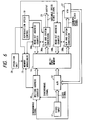
- an image signal processing circuit for processing moving pictures by using such a large capacity image memory
- a digital video signal digitally converted from an analog signal is written into an image memory by one frame portion or a plural-frame portion.
- Addressing of the image memory is controlled by a timing of a synchronous signal of an image signal to be written thereinto.
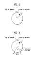
- a memory capacity assigned to one frame portion is, for example, a capacity for (2 n x 2 n ) pixels, as shown in Fig. 1, which has 2 n kinds of horizontal and vertical addresses, respectively.
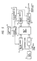
- Reference numeral 19 designates a reproduction speed control circuit for controlling a read-out speed (that is, an output speed of a read-out image) from a memory 14; 34a a read-out address counter for generating a read-out address of the memory 14 under the control of the reproduction speed control circuit 19; 36a a D/A and system converting circuit for converting video data read from the memory 14 by the read-out address counter 34A to to an analog signal and further converting the analog signal to a video signal according to a predetermined system; and 25 an output terminal.
- a writing vector W of the writing address counter 16 when reaching the point a , skips the area between the points a and b and indicates the address at the point b.
- video data memorized in the area between a and b is preserved.
- read-out is permitted or inhibited in the specified block unit.
Claims (15)
- Dispositif de stockage d'informations comprenant :des moyens (12) d'entrée pour fournir en entrée un signal d'information ;une mémoire (14) dans laquelle le signal d'information provenant desdits moyens d'entrée peut être écrit ;des moyens (24, 26) de commande d'adresses d'écriture pour spécifier de façon cyclique des adresses d'écriture de ladite mémoire, auxquelles le signal d'information est écrit ;caractérisé en outre par des moyens (26) d'inhibition pour inhiber des adresses sélectionnées de la mémoire spécifiée par lesdits moyens de commande d'adresses d'écriture, lesdits moyens de commande d'adresses d'écriture étant conçus pour sauter la zone de la mémoire qui est définie par les adresses inhibées et pour écrire en continu le signal d'information avant et après la zone sautée.
- Appareil selon la revendication 1, comportant en outre des moyens (18) de commande d'adresses de lecture pour spécifier des adresses de lecture de ladite mémoire, et des moyens (20) de sortie pour fournir en sortie le signal d'information tel qu'il est lu depuis ladite mémoire.
- Appareil selon la revendication 2, dans lequel le signal d'information est un signal vidéo.
- Appareil selon la revendication 3, dans lequel lesdits moyens de commande d'adresses de lecture peuvent commuter, par unités de trames du signal vidéo la période de mise à jour desdites adresses de lecture afin de faire varier la cadence de reproduction du signal lorsqu'il est lu depuis ladite mémoire.
- Appareil selon la revendication 4, dans lequel lesdits moyens de commande d'adresses de lecture sont capables de spécifier les adresses inhibées par lesdits moyens de commande d'adresses d'écriture afin que la partie du signal d'information qui est stockée dans la zone sautée par les moyens de commande d'adresses d'écriture puisse être lue pendant que le signal d'information est écrit dans les autres parties de la mémoire.
- Appareil selon la revendication 5, comportant en outre des moyens (27) d'enregistrement pour enregistrer des informations fournies en sortie par lesdits moyens de sortie.
- Appareil selon la revendication 6, comportant en outre des moyens (25, 26) pour lever l'inhibition d'écriture définie par lesdits moyens d'inhibition après que des informations ont été lues depuis la zone inhibée de ladite mémoire.
- Appareil selon la revendication 7, dans lequel lesdits moyens de sortie sont conçus pour commander lesdits moyens d'enregistrement pendant que la mémoire fait l'objet d'une lecture.
- Procédé de stockage d'informations consistant :à fournir en entrée (12) un signal d'information ;à écrire le signal d'information dans une mémoire (14) ;à utiliser des moyens (24, 26) de commande d'adresses d'écriture pour spécifier cycliquement des adresses d'écriture de ladite mémoire, auxquelles le signal d'information est écrit ;caractérisé en outre par le fait d'inhiber (26) des adresses sélectionnées de la mémoire, spécifiées par lesdits moyens de commande d'adresses d'écriture, lesdits moyens de commande d'adresses d'écriture étant conçus pour sauter la zone de la mémoire qui est définie par les adresses inhibées et pour écrire en continu le signal d'information avant et après la zone sautée.
- Procédé selon la revendication 9, consistant en outre à spécifier (18) des adresses de lecture de ladite mémoire, et à fournir en sortie (20) le signal d'information tel qu'il est lu depuis ladite mémoire.
- Procédé selon la revendication 9, dans lequel le signal d'information est un signal vidéo.
- Procédé selon la revendication 11, dans lequel lesdits moyens de commande d'adresses de lecture commutent, par unités de trames du signal vidéo, la période de mise à jour desdites adresses de lecture afin de faire varier la cadence de reproduction du signal lorsqu'il est lu depuis ladite mémoire.
- Procédé selon la revendication 12, consistant à spécifier les adresses inhibées par lesdits moyens de commande d'adresses d'écriture de façon que la partie du signal d'information qui est stockée dans la zone sautée par les moyens de commande d'adresses d'écriture puisse être lue pendant que le signal d'information est écrit dans les autres parties de la mémoire.
- Procédé selon la revendication 13, consistant en outre à enregistrer lesdites informations de sortie.
- Procédé selon la revendication 14, consistant en outre à lever l'inhibition d'écriture après que des informations ont été lues depuis la zone inhibée de ladite mémoire.
Applications Claiming Priority (6)
| Application Number | Priority Date | Filing Date | Title |
|---|---|---|---|
| JP94489/91 | 1991-04-24 | ||
| JP3094488A JPH04324775A (ja) | 1991-04-24 | 1991-04-24 | 画像メモリ装置 |
| JP03094489A JP3141421B2 (ja) | 1991-04-24 | 1991-04-24 | 画像記憶装置 |
| JP94487/91 | 1991-04-24 | ||
| JP09448791A JP3288056B2 (ja) | 1991-04-24 | 1991-04-24 | 画像記憶装置 |
| JP94488/91 | 1991-04-24 |
Publications (3)
| Publication Number | Publication Date |
|---|---|
| EP0510968A2 EP0510968A2 (fr) | 1992-10-28 |
| EP0510968A3 EP0510968A3 (en) | 1993-09-15 |
| EP0510968B1 true EP0510968B1 (fr) | 1997-12-17 |
Family
ID=27307563
Family Applications (1)
| Application Number | Title | Priority Date | Filing Date |
|---|---|---|---|
| EP92303654A Expired - Lifetime EP0510968B1 (fr) | 1991-04-24 | 1992-04-23 | Dispositif de mémorisation d'image |
Country Status (3)
| Country | Link |
|---|---|
| US (1) | US5523799A (fr) |
| EP (1) | EP0510968B1 (fr) |
| DE (1) | DE69223543T2 (fr) |
Families Citing this family (14)
| Publication number | Priority date | Publication date | Assignee | Title |
|---|---|---|---|---|
| JP3420257B2 (ja) * | 1992-03-12 | 2003-06-23 | キヤノン株式会社 | 再生装置 |
| JPH06149985A (ja) * | 1992-11-02 | 1994-05-31 | Fujitsu Ltd | 画像情報の処理方式 |
| JP3319209B2 (ja) * | 1995-02-17 | 2002-08-26 | ソニー株式会社 | データ復号化装置 |
| KR100269398B1 (ko) * | 1997-08-30 | 2000-10-16 | 구자홍 | 반복재생을지원하는엠펙비디오디코딩장치및그방법 |
| US6674468B1 (en) * | 1997-10-31 | 2004-01-06 | Canon Kabushiki Kaisha | Image recording apparatus and method for selective prohibition of erasure during recording |
| US6411770B1 (en) * | 1998-07-02 | 2002-06-25 | Sony Corporation | Data recording method and apparatus |
| DE10053683A1 (de) * | 2000-10-28 | 2002-05-08 | Alcatel Sa | Bild-Überwachung |
| JP2003256146A (ja) | 2002-02-26 | 2003-09-10 | Sanyo Electric Co Ltd | データ中継制御装置 |
| JP2007251519A (ja) * | 2006-03-15 | 2007-09-27 | Fujitsu Ltd | ビデオデータ保管装置及びビデオデータ保管方法 |
| US20070250283A1 (en) * | 2006-04-25 | 2007-10-25 | Barnum Melissa A | Maintenance and Calibration Operations for Memories |
| US8310540B2 (en) * | 2006-08-31 | 2012-11-13 | Stellar, Llc | Loop recording with book marking |
| US8928752B2 (en) | 2006-08-31 | 2015-01-06 | Stellar Llc | Recording device with pre-start signal storage capability |
| US7593034B2 (en) | 2006-08-31 | 2009-09-22 | Dekeyser Paul | Loop recording with book marking |
| US9805432B2 (en) | 2014-09-08 | 2017-10-31 | Nxp Usa, Inc. | Data logging system and method |
Family Cites Families (11)
| Publication number | Priority date | Publication date | Assignee | Title |
|---|---|---|---|---|
| US3585610A (en) * | 1968-07-10 | 1971-06-15 | Gulf & Western Industries | Solid state memory and coding system |
| ATE50107T1 (de) * | 1985-08-14 | 1990-02-15 | Siemens Ag | Schaltungsanordnung fuer fernmeldeanlagen, insbesondere fernsprechvermittlungsanlagen, mit abfragestellen zyklisch ansteuernden informationsabfrageeinrichtungen. |
| JP2639650B2 (ja) * | 1987-01-14 | 1997-08-13 | 日本テキサス・インスツルメンツ株式会社 | 半導体装置 |
| JPS63284987A (ja) * | 1987-05-18 | 1988-11-22 | Toshiba Corp | 電子スチルカメラ |
| JP2519302B2 (ja) * | 1988-08-19 | 1996-07-31 | オリンパス光学工業株式会社 | 画像フリ―ズ装置 |
| DE3831366A1 (de) * | 1988-09-15 | 1990-03-29 | Broadcast Television Syst | Speicheranordnung fuer ein digitales videobandgeraet |
| JP2757505B2 (ja) * | 1989-11-28 | 1998-05-25 | ソニー株式会社 | 時間軸補正装置 |
| JP2984311B2 (ja) * | 1990-04-04 | 1999-11-29 | キヤノン株式会社 | 静止画像再生装置 |
| JPH0470077A (ja) * | 1990-07-10 | 1992-03-05 | Konica Corp | 電子スチルカメラの画像記録装置 |
| KR940002573B1 (ko) * | 1991-05-11 | 1994-03-25 | 삼성전자 주식회사 | 광디스크기록재생장치에 있어서 연속재생장치 및 그 방법 |
| JP3257027B2 (ja) * | 1992-04-17 | 2002-02-18 | ソニー株式会社 | 自己診断情報の記録機構を有する情報記録再生装置 |
-
1992
- 1992-04-23 EP EP92303654A patent/EP0510968B1/fr not_active Expired - Lifetime
- 1992-04-23 DE DE69223543T patent/DE69223543T2/de not_active Expired - Lifetime
-
1994
- 1994-07-13 US US08/274,666 patent/US5523799A/en not_active Expired - Lifetime
Also Published As
| Publication number | Publication date |
|---|---|
| EP0510968A3 (en) | 1993-09-15 |
| DE69223543D1 (de) | 1998-01-29 |
| DE69223543T2 (de) | 1998-04-16 |
| US5523799A (en) | 1996-06-04 |
| EP0510968A2 (fr) | 1992-10-28 |
Similar Documents
| Publication | Publication Date | Title |
|---|---|---|
| EP0510968B1 (fr) | Dispositif de mémorisation d'image | |
| US5568165A (en) | Video processing technique using multi-buffer video memory | |
| US5644364A (en) | Media pipeline with multichannel video processing and playback | |
| US5153726A (en) | Recording and editing of moving television pictures | |
| US8314858B2 (en) | Imaging and recording apparatus controlling erasure of data in flash type memory | |
| US5751350A (en) | Dual mode electronic camera having a large recording capacity | |
| US5124692A (en) | Method and apparatus for providing rotation of digital image data | |
| US5452022A (en) | Image signal storage device for a still video apparatus | |
| US6490407B2 (en) | Recording and reproduction of mixed moving and still images | |
| US5438376A (en) | Image processing apparatus and image reception apparatus using the same | |
| US5369441A (en) | Reproducing apparatus with simultaneous parallel processing of different image signals | |
| US4951143A (en) | Memory configuration for unsynchronized input and output data streams | |
| US5319460A (en) | Image signal processing device including frame memory | |
| US6243108B1 (en) | Method and device for processing image data by transferring the data between memories | |
| JP2000083211A (ja) | ディジタル画像デ―タの記憶と取り出しの方法と装置 | |
| US4905099A (en) | Intermediate picture field storage system for variable speed magnetic tape video data read-out | |
| JPH0453148B2 (fr) | ||
| US6151036A (en) | Large capacity data storage device | |
| JPH11103415A (ja) | フレーム変換装置 | |
| JP3141421B2 (ja) | 画像記憶装置 | |
| US20020021885A1 (en) | Method for controlling frames of moving picture and apparatus therefor | |
| JP3038852B2 (ja) | 静止画像復号装置 | |
| JP2918049B2 (ja) | ピクチャ・イン・ピクチャのための記憶方法 | |
| JPH0278385A (ja) | 静止画処理回路 | |
| JP3119366B2 (ja) | 画像処理装置及び方法 |
Legal Events
| Date | Code | Title | Description |
|---|---|---|---|
| PUAI | Public reference made under article 153(3) epc to a published international application that has entered the european phase |
Free format text: ORIGINAL CODE: 0009012 |
|
| AK | Designated contracting states |
Kind code of ref document: A2 Designated state(s): DE ES FR GB IT NL |
|
| PUAL | Search report despatched |
Free format text: ORIGINAL CODE: 0009013 |
|
| AK | Designated contracting states |
Kind code of ref document: A3 Designated state(s): DE ES FR GB IT NL |
|
| 17P | Request for examination filed |
Effective date: 19940204 |
|
| 17Q | First examination report despatched |
Effective date: 19960215 |
|
| GRAG | Despatch of communication of intention to grant |
Free format text: ORIGINAL CODE: EPIDOS AGRA |
|
| GRAG | Despatch of communication of intention to grant |
Free format text: ORIGINAL CODE: EPIDOS AGRA |
|
| GRAH | Despatch of communication of intention to grant a patent |
Free format text: ORIGINAL CODE: EPIDOS IGRA |
|
| GRAH | Despatch of communication of intention to grant a patent |
Free format text: ORIGINAL CODE: EPIDOS IGRA |
|
| GRAA | (expected) grant |
Free format text: ORIGINAL CODE: 0009210 |
|
| AK | Designated contracting states |
Kind code of ref document: B1 Designated state(s): DE ES FR GB IT NL |
|
| PG25 | Lapsed in a contracting state [announced via postgrant information from national office to epo] |
Ref country code: IT Free format text: LAPSE BECAUSE OF FAILURE TO SUBMIT A TRANSLATION OF THE DESCRIPTION OR TO PAY THE FEE WITHIN THE PRE;WARNING: LAPSES OF ITALIAN PATENTS WITH EFFECTIVE DATE BEFORE 2007 MAY HAVE OCCURRED AT ANY TIME BEFORE 2007. THE CORRECT EFFECTIVE DATE MAY BE DIFFERENT FROM THE ONE RECORDED.SCRIBED TIME-LIMIT Effective date: 19971217 Ref country code: ES Free format text: THE PATENT HAS BEEN ANNULLED BY A DECISION OF A NATIONAL AUTHORITY Effective date: 19971217 |
|
| REF | Corresponds to: |
Ref document number: 69223543 Country of ref document: DE Date of ref document: 19980129 |
|
| ET | Fr: translation filed | ||
| PLBE | No opposition filed within time limit |
Free format text: ORIGINAL CODE: 0009261 |
|
| STAA | Information on the status of an ep patent application or granted ep patent |
Free format text: STATUS: NO OPPOSITION FILED WITHIN TIME LIMIT |
|
| 26N | No opposition filed | ||
| REG | Reference to a national code |
Ref country code: GB Ref legal event code: IF02 |
|
| PGFP | Annual fee paid to national office [announced via postgrant information from national office to epo] |
Ref country code: GB Payment date: 20100319 Year of fee payment: 19 |
|
| PGFP | Annual fee paid to national office [announced via postgrant information from national office to epo] |
Ref country code: FR Payment date: 20100430 Year of fee payment: 19 |
|
| PGFP | Annual fee paid to national office [announced via postgrant information from national office to epo] |
Ref country code: NL Payment date: 20100415 Year of fee payment: 19 Ref country code: DE Payment date: 20100430 Year of fee payment: 19 |
|
| REG | Reference to a national code |
Ref country code: NL Ref legal event code: V1 Effective date: 20111101 |
|
| GBPC | Gb: european patent ceased through non-payment of renewal fee |
Effective date: 20110423 |
|
| REG | Reference to a national code |
Ref country code: FR Ref legal event code: ST Effective date: 20111230 |
|
| PG25 | Lapsed in a contracting state [announced via postgrant information from national office to epo] |
Ref country code: DE Free format text: LAPSE BECAUSE OF NON-PAYMENT OF DUE FEES Effective date: 20111101 Ref country code: NL Free format text: LAPSE BECAUSE OF NON-PAYMENT OF DUE FEES Effective date: 20111101 Ref country code: FR Free format text: LAPSE BECAUSE OF NON-PAYMENT OF DUE FEES Effective date: 20110502 |
|
| REG | Reference to a national code |
Ref country code: DE Ref legal event code: R119 Ref document number: 69223543 Country of ref document: DE Effective date: 20111101 |
|
| PG25 | Lapsed in a contracting state [announced via postgrant information from national office to epo] |
Ref country code: GB Free format text: LAPSE BECAUSE OF NON-PAYMENT OF DUE FEES Effective date: 20110423 |