EP0510968B1 - An image memorizing device - Google Patents
An image memorizing device Download PDFInfo
- Publication number
- EP0510968B1 EP0510968B1 EP92303654A EP92303654A EP0510968B1 EP 0510968 B1 EP0510968 B1 EP 0510968B1 EP 92303654 A EP92303654 A EP 92303654A EP 92303654 A EP92303654 A EP 92303654A EP 0510968 B1 EP0510968 B1 EP 0510968B1
- Authority
- EP
- European Patent Office
- Prior art keywords
- memory
- read
- writing
- information signal
- control means
- Prior art date
- Legal status (The legal status is an assumption and is not a legal conclusion. Google has not performed a legal analysis and makes no representation as to the accuracy of the status listed.)
- Expired - Lifetime
Links
Images


Classifications
-
- G—PHYSICS
- G11—INFORMATION STORAGE
- G11C—STATIC STORES
- G11C8/00—Arrangements for selecting an address in a digital store
-
- G—PHYSICS
- G11—INFORMATION STORAGE
- G11C—STATIC STORES
- G11C8/00—Arrangements for selecting an address in a digital store
- G11C8/20—Address safety or protection circuits, i.e. arrangements for preventing unauthorized or accidental access
-
- H—ELECTRICITY
- H04—ELECTRIC COMMUNICATION TECHNIQUE
- H04N—PICTORIAL COMMUNICATION, e.g. TELEVISION
- H04N5/00—Details of television systems
- H04N5/76—Television signal recording
- H04N5/907—Television signal recording using static stores, e.g. storage tubes or semiconductor memories
-
- H—ELECTRICITY
- H04—ELECTRIC COMMUNICATION TECHNIQUE
- H04N—PICTORIAL COMMUNICATION, e.g. TELEVISION
- H04N5/00—Details of television systems
- H04N5/76—Television signal recording
- H04N5/91—Television signal processing therefor
-
- H—ELECTRICITY
- H04—ELECTRIC COMMUNICATION TECHNIQUE
- H04N—PICTORIAL COMMUNICATION, e.g. TELEVISION
- H04N5/00—Details of television systems
- H04N5/76—Television signal recording
- H04N5/91—Television signal processing therefor
- H04N5/93—Regeneration of the television signal or of selected parts thereof
- H04N5/937—Regeneration of the television signal or of selected parts thereof by assembling picture element blocks in an intermediate store
Definitions
- the present invention relates to an image memorizing device, and more particularly, to an image memorizing device for processing a large amount of image data such as moving pictures by using large capacity memories.
- Such an image memory tends to have a larger capacity and now becomes sufficiently usable as a recording medium for moving pictures.
- a solid state memory such as a dynamic random access memory is used as a recording medium for moving pictures, there are advantages, e.g., a search can be performed at a high speed; data can be readily rearranged in the memory; and data can be recorded and reproduced at an arbitrary speed.
- an image signal processing circuit for processing moving pictures by using such a large capacity image memory
- a digital video signal digitally converted from an analog signal is written into an image memory by one frame portion or a plural-frame portion.
- Addressing of the image memory is controlled by a timing of a synchronous signal of an image signal to be written thereinto.
- a memory capacity assigned to one frame portion is, for example, a capacity for (2 n x 2 n ) pixels, as shown in Fig. 1, which has 2 n kinds of horizontal and vertical addresses, respectively.
- Reference numeral 19 designates a reproduction speed control circuit for controlling a read-out speed (that is, an output speed of a read-out image) from a memory 14; 34a a read-out address counter for generating a read-out address of the memory 14 under the control of the reproduction speed control circuit 19; 36a a D/A and system converting circuit for converting video data read from the memory 14 by the read-out address counter 34A to to an analog signal and further converting the analog signal to a video signal according to a predetermined system; and 25 an output terminal.
- a writing vector W of the writing address counter 16 when reaching the point a , skips the area between the points a and b and indicates the address at the point b.
- video data memorized in the area between a and b is preserved.
- read-out is permitted or inhibited in the specified block unit.
Description
- The present invention relates to an image memorizing device, and more particularly, to an image memorizing device for processing a large amount of image data such as moving pictures by using large capacity memories.
- There have been known a kind of memory which is adapted to cyclically memorize data its storage area by linking the end address of the storage area to the start address of the same and an addressing control therefor as a so-called ring memory, and an image memorizing device for storing image signals in such a ring memory has been also known.
- In the ring memory, previously memorized information cannot be protected from being overwritten by next information due to the nature of its addressing control. For example, when moving pictures are to be memorized, a previously memorized image is lost by overwriting the next image, so that non-sequential images in terms of time cannot be obtained.
- Incidentally, such an image memory tends to have a larger capacity and now becomes sufficiently usable as a recording medium for moving pictures. If a solid state memory such as a dynamic random access memory is used as a recording medium for moving pictures, there are advantages, e.g., a search can be performed at a high speed; data can be readily rearranged in the memory; and data can be recorded and reproduced at an arbitrary speed.
- Generally, in an image signal processing circuit for processing moving pictures by using such a large capacity image memory, a digital video signal digitally converted from an analog signal, as it is, is written into an image memory by one frame portion or a plural-frame portion. Addressing of the image memory is controlled by a timing of a synchronous signal of an image signal to be written thereinto.
- Conventionally, since an addressing control of an image memory is defined by a synchronizing timing of a synchronous signal, quite a few unused portion, as indicated by hatching in Fig. 1, are produced and left useless. Each unused portion may occupy a noticeable amount depending upon the number of horizontal pixels and the number of horizontal lines.
- Specifically, a memory capacity assigned to one frame portion is, for example, a capacity for (2n x 2n) pixels, as shown in Fig. 1, which has 2n kinds of horizontal and vertical addresses, respectively. The number of scanning lines is 525 in the case of an NTSC signal and 625 in the case of a PAL signal, so that approximately 700 - 800 of horizontal pixels are required. Therefore, substituting 10 for n, approximately 1024 (= 210) addresses are required for the horizontal pixels.
- Further, in the case of a high definition signal, substituting 11 for n, 2048 addresses are required for each of the horizontal and vertical addresses.
- Thus, the unused portions as shown in Fig. 1 include an extremely large amount of address, thereby exhibiting low memory utilisation efficiency. However, unless the address is reset in the horizontal scanning line units or frame units, management of the address in a large capacity memory becomes extremely difficult.
- In view of the above-mentioned background, it is a concern of the present invention to provide an image memorizing apparatus which is capable of writing a new moving image into a single large capacity memory while preserving a desired portion of moving images which have previously been written in the same memory.
- It is another concern of the present invention to provide an image memorizing device which is capable of largely improving a using efficiency of a memory capacity in spite of relatively easy addressing management.
- An article by J.R. Crook et al, entitled "Solid State Video Recorder" and published in "International Broadcasting Convention, September 1988, London, UK" discloses a digital video recorded system having a memory a portion of which can act as a delay store and into which video data can be written cyclically and read out after a predetermined delay.
- In accordance with aspects of the present invention there is provided an information storage device as set out in
claim 1 and an information storage method as set out in claim 9. - Further features of the present invention will become apparent from the following detailed description of embodiments with reference to accompanying drawings.
-
- Fig. 1 is a diagram used for explaining an ordinary memory using situation;
- Fig. 2 is a block diagram showing the structure of an image memorizing apparatus as an embodiment of the present invention;
- Fig. 3 is a diagram used for explaining the operation of a memory shown in Fig. 2;
- Fig. 4 is a diagram used for explaining the operation of the memory in Fig. 2 when a writing inhibited area is set therein;
- Fig. 5 is a block diagram showing the structure of an image memorizing device as another embodiment of the present invention;
- Fig. 6 is a block diagram showing the structure of an image memorizing device as a further embodiment of the present invention;
- Fig. 7 is a block diagram showing the structure of an image memorizing device as a further embodiment of the present invention;
- Fig. 8 is a diagram used for explaining another using manner of the memory in each embodiment;
- Fig. 9 is a block diagram showing the structure of an image memorizing device as another embodiment of the present invention; and
- Fig. 10 is a diagram showing a using situation of a memory in the device of the embodiment shown in Fig. 9.
- Embodiments of the present invention will hereinafter be described with reference to the accompanying drawings.
- Fig. 2 is a block diagram showing the structure of an image memorizing device according to an embodiment of the present invention which is applied to output processing of a video camera.
Reference numeral 10 designates a video camera; 12 an analog-to-digital (A/D) convertor for digitizing a video signal outputted from thevideo camera 10; and 14 a multi-port random access memory for memorizing a digital video signal outputted from the A/D convertor 12. In the present embodiment, thememory 14 may have a capacity of memorizing a several-second to approximately 50-second portion of video signals. -
Reference numeral 16 designates a writing address counter for generating a writing address of thememory 14 in response to a synchronous signal multiplexed with the video signal outputted from thevideo camera 10; 18 a read-out counter for generating a read-out address of thememory 14; 20 a digital-to-analog (D/A) convertor for converting video data read from thememory 14 to an analog signal; and 22 an output terminal. - Also,
reference numeral 24 designates a memory managing circuit for controlling thewriting address counter 16 and the read-out address counter 18 in accordance with a writing inhibited area registered in thememory 14. The user can select through anoperation unit 26 and register in the memory managing circuit 24 a writing inhibited area in thememory 14, that is, an arbitrary number of images to be preserved. - Next, the operation of the above-mentioned image memorizing device will be described. A video signal outputted from the
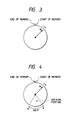
video camera 10 is digitized by the A/D convertor 12 and written into addresses indicated by thewriting address counter 16. The address of the writing address counter l6 is incremented by the synchronous signal multiplexed with the video signal. Thewriting address counter 16 returns to the start address of thememory 14 by an increment after the end address of thememory 14 has reached. Thus, thememory 14 operates as a ring memory. Fig. 3 schematically illustrates the writing addresses of thememory 14. A writing position is represented as a vector W which rotates at an angular velocity ω. - If there is a scene to be preserved during making a film, the
operation unit 26 is operated to specify a portion to be preserved immediately after the scene has been written into thememory 14. With this operation, thememory managing circuit 24 instructs a writing inhibition to addresses in thememory 14 corresponding to the portion to be preserved. In this event, an arbitrary address area of thememory 14 can be specified, and the size of the area can be arbitrarily set. - After completing the registration (setting), film-making is resumed. The
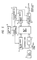
writing address counter 16 skips writing addresses for the address area registered in thememory managing circuit 24. For example, if it is assumed that an area between points a and b shown in Fig. 4 is registered as a writing inhibited area, the writing vector W, when reaching the point a, skips the area between the points a and b, and then writes data at the point b. Thus, video data memorized in the area between the points a and b is preserved. - Next, description will be made as to another embodiment where the present invention is applied to processing of an n-times speed video signal. Fig. 5 shows the structure of the embodiment in a block form. The constituents identical to those in Fig. 2 are designated the same reference numerals.
Reference numeral 30 designates a video camera which is capable of making a film at a field frequency n times that of a standard television signal, the output video signal of which is written into amemory 14 by an A/D convertor 12, awriting address counter 16 and amemory managing circuit 24, similarly to the device shown in Fig. 2. A slowreproduction control circuit 32 controls a read-out address counter 34 to read data from thememory 14 at an arbitrary speed and converts the read data to a standard television signal by a D/A converting andsystem converting circuit 36. More specifically, in the present embodiment one field portion of a video signal is read out in one field period of a standard television signal, however, in a l/n slow reproduction mode, a read-out field address is updated once per field period. - In a normal reproduction mode, a field address read out once per field period is advanced by n fields. Further, in a 1/2n slow reproduction mode, a signal in the one and same field is repeatedly read out twice over two field periods, and a read-out field address is updated once per two field periods. By thus constructing the device, a video signal can be outputted at an arbitrary speed.
- As described above, according to the device of the present invention disclosed in Figs. 2 to 5, by setting a particular address area of a memory as a writing inhibited area, it is possible to memorize two or more kinds of different moving images in a single memory and read them therefrom.
- Next, another embodiment of the present invention will be described.
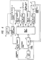
- Fig. 6 is a block diagram showing the structure of an image memorizing device as another embodiment of the present invention, wherein constituents similar to those in Fig. 5 are designated the same reference numeral, and explanation thereof will be omitted.
-
Reference numeral 19 designates a reproduction speed control circuit for controlling a read-out speed (that is, an output speed of a read-out image) from amemory 14; 34a a read-out address counter for generating a read-out address of thememory 14 under the control of the reproductionspeed control circuit 19; 36a a D/A and system converting circuit for converting video data read from thememory 14 by the read-out address counter 34A to to an analog signal and further converting the analog signal to a video signal according to a predetermined system; and 25 an output terminal. - Also,
reference numeral 27 designates a video tape recorder (VTR) for recording an image to be preserved; 25 a memory managing circuit for reading out an image to be preserved to have theVTR 27 record the same and for inhibiting writing into a recording area in which the image to be preserved is memorized for a necessary period; 34b a read-out address counter for generating a read-out address of thememory 14 under the control of the memory managing circuit 28; and 36b a D/A and system converting circuit for converting video data read from thememory 14 by the read-outaddress counter 34b to an analog signal and further converting the analog signal to a video signal according to a predetermined system. An output from the D/A andsystem converting circuit 36b is supplied to theVTR 27. - For re-loading a video signal recorded by the
VTR 27 to thememory 14, a video signal output reproduced by theVTR 27 is applied to the A/D convertor 12, while a synchronous signal multiplexed with the reproduced video signal is applied to thewriting address counter 16. - Next, the operation of the device shown in Fig. 6 will be described.
Reference numeral 11 designates a video input terminal to which a video signal is inputted from a video camera. The operation for writing a video signal from thevideo input terminal 11 into thememory 14 is entirely the same as the operation for memorizing a video signal from thevideo camera 10 into thememory 14 of Fig. 2. - The
memory 14, as described above, is handled as a ring memory. If a writing inhibited area is not set therein, the memory l4 stores a video signal of a past period T from the current time, wherein reference letter T represents a recordable period of thememory 14. - The whole recording area of the
memory 14 is divided into n blocks in arbitrary sizes, and thememory managing circuit 25 holds this division information. Thememory managing circuit 25 controls writing by the writingaddress counter 16, and read-out by the read-out address counters 20, 30 in this block unit. - For example, if the area between the points a and b shown in Fig. 4 is designated a
block # 1 and the remainingarea block # 2 by anoperation unit 26, and if theblock # 1 is specified as a writing inhibited area, a writing vector W of thewriting address counter 16, when reaching the point a, skips the area between the points a and b and indicates the address at the point b. Thus, video data memorized in the area between a and b is preserved. Also, with respect to read-out, read-out is permitted or inhibited in the specified block unit. - Next, a back-up operation will be described. Assume that video data is being written into a certain block, in the manner described above. Data is read from a writing inhibited block (a block in which an image to be preserved is recorded) other than the block into which video data is being written by the read-out
address counter 34b, and converted to an analog signal and further to a signal according to the standard system by the D/A andsystem converting circuit 36b. Then, in association with an output operation of the D/A andsystem converting circuit 36b, theVTR 27 is operated to record the video signal converted to the standard system. Specifically, the D/A andsystem converting circuit 36b controls theVTR 27 to start and stop the recording. By these operations, the video signal to be preserved can be backed up on a recording medium by theVTR 27. - After the video signal has been backed up the
VTR 27, when the read-outaddress counter 34b supplies thememory managing circuit 25 with a signal indicative of the termination of this back-up operation, thememory managing circuit 25 permits writing into the writing inhibited block from which the video signal has been read. - Since a video signal memorized in the
memory 14 need to be backed up, a video signal read from the D/A andsystem converting circuit 36b is preferably a video signal at a standard speed. In the device shown in Fig. 6, since a video signal written into thememory 14 is a standard video signal, a field address is updated by thecounter 34b once per field period of this standard video signal, whereby a normal reproduction can be performed. - On the other hand, a video signal may be outputted to an
output terminal 29 at one of various speeds as the user desires. Specifically, the reproductionspeed control circuit 19 can vary the updated period of the field address of thecounter 34a via theoperation unit 26. For example, when a slow motion reproduction is to be performed, the field address is updated once per several field periods, and video signals at the same field addresses are repeatedly read out during these several fields. Also, when a high speed search is to be performed, the field address may be advanced by several fields once per field period. - Fig. 7 is a block diagram showing the structure of a second embodiment of the present invention. Constituents having functions similar or analogous to those in Fig. 6 are designated the same reference numerals. As an image source, there is connected a
high speed camera 40 which outputs a video signal at a field frequency n times that of the standard television system, and a highspeed buffer memory 42 is connected between amulti-port memory 14 and a D/A andsystem converting circuit 36b. A transfer speed from thememory 14 to thebuffer memory 42 is the same as a speed at which data is written into thememory 14, that is, n times a transfer speed from the D/A andsystem converting circuit 36b to aVTR 26. The D/A andsystem converting circuit 36b sequentially converts video data from thebuffer memory 42 to a standard video signal which in turn is recorded on a video tape by theVTR 27. - Thus, even a high speed video signal can be backed up at a high speed, and accordingly the memory can be highly efficiently utilized.
- Although in the above-mentioned embodiment, the
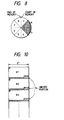
memory 14 is divided into two blocks respectively having a different size from each other and managed, it may be divided into m banks of a fixed length (for example eight banks 1 - 8 in Fig. 8), and the presence or absence of back-up may be managed in the bank units. For example, if an area between points a and b is to be preserved in Fig. 8, writing addresses ofbanks # 2, #3 including that area are skipped, and images recorded therein are backed up on a video tape. Such banks of a fixed length can alleviate the load of amemory managing circuit 25. - As will be readily understood from the above explanation, according to the device described in connection with Figs. 6 - 8, an important image memorized in a soild-state memory device can be preserved or backed up on a separate recording medium without being erased by a subsequent image. This back-up operation allows an efficient utilization of a memory capacity of the solid-state memory device. Further, since writing and read-out are simultaneously performed, data can be preserved on a separate recording medium at a high speed.
- Fig. 9 is a block diagram showing the structure of a further embodiment of the present invention.
Reference numeral 110 designates an input terminal to which an image signal (moving pictures or a still image) is fed from a video camera or a video reproducing apparatus; 112 an input circuit comprising an A/D convertor for digitizing an image from theinput terminal 110; 114 an FIFO (First-In First-Out) memory (buffer memory) for a synchronously supplying an output of theinput circuit 112 to abus 116; 118 an image memory; and 120 an address generating circuit for generating an address of theimage memory 118. Thebus 116 comprises a data bus, a plurality of control signal lines and a clock line. -
Reference numerals respective output circuits image memory 118 and inputted through thebus 116. Theoutput circuits Reference numerals -
Reference numerals output circuits FIFO memories FIFO memories image memory 118 via thebus 116; 140, 142, 144 trigger generating circuits for generating a request for transferring every predetermined amount of data between the input andoutput circuits FIFO memories -
Reference numeral 152 designates a memory control circuit for arbitrating a request for data transfer between the respective input andoutput circuits image memory 118 and theFIFO memories - Next, the operation of the present embodiment will be described in connection with a case where an image signal inputted to the
input terminal 110 is stored in theimage memory 118, by way of example. - The user indicates from the
operation unit 154 thememory control circuit 152 to store input image data to theimage memory 118. Thememory control circuit 152 instructs thepulse generating circuit 134 of writing an output of theinput circuit 112 into theFIFO memory 114. Thepulse generating circuit 134 generates a control signal for writing into theFIFO memory 114 in synchronism with a synchronous signal of an image signal inputted from theinput terminal 110. Thetrigger generating circuit 140 in turn transmits a trigger signal to the trigger counter l46 and thememory control circuit 152 every time a predetermined amount of image data less than one frame portion of image (hereinafter referred to the memory unit) is written into theFIFO memory 114. Thetrigger counter 146 counts this trigger signal and supplies the memory control circuit 52 with the number of counted trigger signals. - The
memory control circuit 152, in response to the trigger signal from thetrigger generating circuit 140, has thetrigger counter 146 output the number of counted trigger signals to theaddress generating circuit 120 and simultaneously transfer the number of counted trigger signals to theimage memory 118 via thebus 116. Theaddress generating circuit 120 generates an address for each of data in the memory unit, at which image data from theFIFO memory 114 is written into theimage memory 118. Assuming here that the foregoing predetermined amount is equal to 2n pixels, a memory using situation is as shown in Fig. 10. - By the above operations, image data is close-packed in the
image memory 118, whereby unused portions are left only in hatched areas shown in Fig. 10. Thus, the unused portion can be largely reduced. Incidentally, blocks #1, #2, #3 respectively indicate image data of one frame portion. - Read-out of image data from the
image memory 118 to theoutput circuits image memory 118 and theFIFO memories memory control circuit 152 arbitrates respective transfer requests so as to prevent the transfer requests from being simultaneously generated. - As will be readily understood from the above explanation, the embodiment of Fig. 9 provides an image memorizing device which can reduce unused portions, facilitate the address management of the
memory 118, and present a high utilizating efficiency.
Claims (15)
- An information storage device comprising:input means (12) for inputting an information signal;a memory (14) into which the information signal from said input means can be written;writing address control means (24, 26) for cyclically specifying writing addresses of said memory 1 to which the information signal is written;and characterised by inhibiting means (26) for inhibiting selected addresses of the memory specified by said writing address control means whereby said writing address control means is adapted to skip the area of the memory defined by the inhibited addresses and continuously to write the information signal before and after the skipped area.
- Apparatus according to claim 1, and including read-out address control means (18) for specifying read-out addresses of said memory, and output means (20) for outputting the information signal as read from said memory.
- Apparatus according to claim 2, wherein the information signal is a video signal.
- Apparatus according to claim 3, wherein said read-out address control means can switch in frame units of the video signal the update period of said read-out addresses so as to vary the reproduction rate of the signal when read from said memory.
- Apparatus according to claim 4, wherein said read-out address control means is capable of specifying the addresses inhibited by said writing address control means so that the part of the information signal stored in the area skipped by the writing address control means can be read whilst the information signal is being written to the other parts of the memory.
- Apparatus according to claim 5, and including recording means (27) for recording information output by said output means.
- Apparatus according to claim 6, and including means (25, 26) for releasing the writing inhibition set by said inhibiting means after information has been read from the inhibited area of said memory.
- Apparatus according to claim 7, wherein said output means is adapted to control said recording means whilst the memory is being read.
- A method of storing information comprising:inputting (12) an information signal;writing the information signal in a memory (14);utilising writing address control means (24, 26) to cyclically specify writing addresses of said memory to which the information signal is written;and characterised by inhibiting (26) selected addresses of the memory specified by said writing address control means whereby said writing address control means is adapted to skip the area of the memory defined by the inhibited addresses and continuously to write the information signal before and after the skipped area.
- A method according to claim 9, and including specifying (18) read-out addresses of said memory, and outputting (20) the information signal as read from said memory.
- A method according to claim 9, wherein the information signal is a video signal.
- A method according to claim 11, wherein said read-out address control means switches, in framed units of the video signal, the update period of said read-out addresses so as to vary the reproduction rate of the signal when read from said memory.
- A method according to claim 12, including specifying the addresses inhibited by said writing address control means so that the part of the information signal stored in the area skipped by the writing address control means can be read whilst the information signal is being written to the other parts of the memory.
- A method according to claim 13, and including recording said output information.
- A method according to claim 14, and releasing the writing inhibition after information has been read from the inhibited area of said memory.
Applications Claiming Priority (6)
| Application Number | Priority Date | Filing Date | Title |
|---|---|---|---|
| JP94489/91 | 1991-04-24 | ||
| JP94487/91 | 1991-04-24 | ||
| JP94488/91 | 1991-04-24 | ||
| JP3094488A JPH04324775A (en) | 1991-04-24 | 1991-04-24 | Picture memory device |
| JP09448791A JP3288056B2 (en) | 1991-04-24 | 1991-04-24 | Image storage device |
| JP03094489A JP3141421B2 (en) | 1991-04-24 | 1991-04-24 | Image storage device |
Publications (3)
| Publication Number | Publication Date |
|---|---|
| EP0510968A2 EP0510968A2 (en) | 1992-10-28 |
| EP0510968A3 EP0510968A3 (en) | 1993-09-15 |
| EP0510968B1 true EP0510968B1 (en) | 1997-12-17 |
Family
ID=27307563
Family Applications (1)
| Application Number | Title | Priority Date | Filing Date |
|---|---|---|---|
| EP92303654A Expired - Lifetime EP0510968B1 (en) | 1991-04-24 | 1992-04-23 | An image memorizing device |
Country Status (3)
| Country | Link |
|---|---|
| US (1) | US5523799A (en) |
| EP (1) | EP0510968B1 (en) |
| DE (1) | DE69223543T2 (en) |
Families Citing this family (14)
| Publication number | Priority date | Publication date | Assignee | Title |
|---|---|---|---|---|
| JP3420257B2 (en) * | 1992-03-12 | 2003-06-23 | キヤノン株式会社 | Playback device |
| JPH06149985A (en) * | 1992-11-02 | 1994-05-31 | Fujitsu Ltd | Processing system for image information |
| JP3319209B2 (en) * | 1995-02-17 | 2002-08-26 | ソニー株式会社 | Data decryption device |
| KR100269398B1 (en) * | 1997-08-30 | 2000-10-16 | 구자홍 | Mpeg video decoder for supporting replay and decoding method thereof |
| US6674468B1 (en) * | 1997-10-31 | 2004-01-06 | Canon Kabushiki Kaisha | Image recording apparatus and method for selective prohibition of erasure during recording |
| US6411770B1 (en) * | 1998-07-02 | 2002-06-25 | Sony Corporation | Data recording method and apparatus |
| DE10053683A1 (en) * | 2000-10-28 | 2002-05-08 | Alcatel Sa | Image monitoring |
| JP2003256146A (en) | 2002-02-26 | 2003-09-10 | Sanyo Electric Co Ltd | Data relay control device |
| JP2007251519A (en) * | 2006-03-15 | 2007-09-27 | Fujitsu Ltd | Video data storage device and video data storage method |
| US20070250283A1 (en) * | 2006-04-25 | 2007-10-25 | Barnum Melissa A | Maintenance and Calibration Operations for Memories |
| US7593034B2 (en) | 2006-08-31 | 2009-09-22 | Dekeyser Paul | Loop recording with book marking |
| US8928752B2 (en) | 2006-08-31 | 2015-01-06 | Stellar Llc | Recording device with pre-start signal storage capability |
| US8310540B2 (en) * | 2006-08-31 | 2012-11-13 | Stellar, Llc | Loop recording with book marking |
| US9805432B2 (en) | 2014-09-08 | 2017-10-31 | Nxp Usa, Inc. | Data logging system and method |
Family Cites Families (11)
| Publication number | Priority date | Publication date | Assignee | Title |
|---|---|---|---|---|
| US3585610A (en) * | 1968-07-10 | 1971-06-15 | Gulf & Western Industries | Solid state memory and coding system |
| ATE50107T1 (en) * | 1985-08-14 | 1990-02-15 | Siemens Ag | CIRCUIT ARRANGEMENT FOR TELECOMMUNICATION SYSTEMS, IN PARTICULAR TELEPHONE EXCHANGE SYSTEMS, WITH INFORMATION REQUEST DEVICES CYCLICLY CONTROLLING REQUEST POINTS. |
| JP2639650B2 (en) * | 1987-01-14 | 1997-08-13 | 日本テキサス・インスツルメンツ株式会社 | Semiconductor device |
| JPS63284987A (en) * | 1987-05-18 | 1988-11-22 | Toshiba Corp | Electronic still camera |
| JP2519302B2 (en) * | 1988-08-19 | 1996-07-31 | オリンパス光学工業株式会社 | Image freezing device |
| DE3831366A1 (en) * | 1988-09-15 | 1990-03-29 | Broadcast Television Syst | MEMORY ARRANGEMENT FOR A DIGITAL VIDEO TAPE |
| JP2757505B2 (en) * | 1989-11-28 | 1998-05-25 | ソニー株式会社 | Time axis correction device |
| JP2984311B2 (en) * | 1990-04-04 | 1999-11-29 | キヤノン株式会社 | Still image playback device |
| JPH0470077A (en) * | 1990-07-10 | 1992-03-05 | Konica Corp | Picture recording device |
| KR940002573B1 (en) * | 1991-05-11 | 1994-03-25 | 삼성전자 주식회사 | Optical disk recording playback device and method |
| JP3257027B2 (en) * | 1992-04-17 | 2002-02-18 | ソニー株式会社 | Information recording / reproducing device having self-diagnosis information recording mechanism |
-
1992
- 1992-04-23 EP EP92303654A patent/EP0510968B1/en not_active Expired - Lifetime
- 1992-04-23 DE DE69223543T patent/DE69223543T2/en not_active Expired - Lifetime
-
1994
- 1994-07-13 US US08/274,666 patent/US5523799A/en not_active Expired - Lifetime
Also Published As
| Publication number | Publication date |
|---|---|
| DE69223543T2 (en) | 1998-04-16 |
| EP0510968A2 (en) | 1992-10-28 |
| DE69223543D1 (en) | 1998-01-29 |
| EP0510968A3 (en) | 1993-09-15 |
| US5523799A (en) | 1996-06-04 |
Similar Documents
| Publication | Publication Date | Title |
|---|---|---|
| EP0510968B1 (en) | An image memorizing device | |
| US5568165A (en) | Video processing technique using multi-buffer video memory | |
| US5644364A (en) | Media pipeline with multichannel video processing and playback | |
| US5153726A (en) | Recording and editing of moving television pictures | |
| US8314858B2 (en) | Imaging and recording apparatus controlling erasure of data in flash type memory | |
| US5751350A (en) | Dual mode electronic camera having a large recording capacity | |
| US5124692A (en) | Method and apparatus for providing rotation of digital image data | |
| US5452022A (en) | Image signal storage device for a still video apparatus | |
| US6490407B2 (en) | Recording and reproduction of mixed moving and still images | |
| US5438376A (en) | Image processing apparatus and image reception apparatus using the same | |
| US5369441A (en) | Reproducing apparatus with simultaneous parallel processing of different image signals | |
| US4951143A (en) | Memory configuration for unsynchronized input and output data streams | |
| US5319460A (en) | Image signal processing device including frame memory | |
| US6243108B1 (en) | Method and device for processing image data by transferring the data between memories | |
| JP2000083211A (en) | Method and device for storing and extracting digital image data | |
| US4905099A (en) | Intermediate picture field storage system for variable speed magnetic tape video data read-out | |
| JPH0453148B2 (en) | ||
| US6151036A (en) | Large capacity data storage device | |
| JPH11103415A (en) | Frame converting device | |
| JP3141421B2 (en) | Image storage device | |
| US20020021885A1 (en) | Method for controlling frames of moving picture and apparatus therefor | |
| JP3038852B2 (en) | Still image decoding device | |
| JP2918049B2 (en) | Storage method for picture-in-picture | |
| JPH0278385A (en) | Still picture processing circuit | |
| JP2753010B2 (en) | Moving image display method |
Legal Events
| Date | Code | Title | Description |
|---|---|---|---|
| PUAI | Public reference made under article 153(3) epc to a published international application that has entered the european phase |
Free format text: ORIGINAL CODE: 0009012 |
|
| AK | Designated contracting states |
Kind code of ref document: A2 Designated state(s): DE ES FR GB IT NL |
|
| PUAL | Search report despatched |
Free format text: ORIGINAL CODE: 0009013 |
|
| AK | Designated contracting states |
Kind code of ref document: A3 Designated state(s): DE ES FR GB IT NL |
|
| 17P | Request for examination filed |
Effective date: 19940204 |
|
| 17Q | First examination report despatched |
Effective date: 19960215 |
|
| GRAG | Despatch of communication of intention to grant |
Free format text: ORIGINAL CODE: EPIDOS AGRA |
|
| GRAG | Despatch of communication of intention to grant |
Free format text: ORIGINAL CODE: EPIDOS AGRA |
|
| GRAH | Despatch of communication of intention to grant a patent |
Free format text: ORIGINAL CODE: EPIDOS IGRA |
|
| GRAH | Despatch of communication of intention to grant a patent |
Free format text: ORIGINAL CODE: EPIDOS IGRA |
|
| GRAA | (expected) grant |
Free format text: ORIGINAL CODE: 0009210 |
|
| AK | Designated contracting states |
Kind code of ref document: B1 Designated state(s): DE ES FR GB IT NL |
|
| PG25 | Lapsed in a contracting state [announced via postgrant information from national office to epo] |
Ref country code: IT Free format text: LAPSE BECAUSE OF FAILURE TO SUBMIT A TRANSLATION OF THE DESCRIPTION OR TO PAY THE FEE WITHIN THE PRE;WARNING: LAPSES OF ITALIAN PATENTS WITH EFFECTIVE DATE BEFORE 2007 MAY HAVE OCCURRED AT ANY TIME BEFORE 2007. THE CORRECT EFFECTIVE DATE MAY BE DIFFERENT FROM THE ONE RECORDED.SCRIBED TIME-LIMIT Effective date: 19971217 Ref country code: ES Free format text: THE PATENT HAS BEEN ANNULLED BY A DECISION OF A NATIONAL AUTHORITY Effective date: 19971217 |
|
| REF | Corresponds to: |
Ref document number: 69223543 Country of ref document: DE Date of ref document: 19980129 |
|
| ET | Fr: translation filed | ||
| PLBE | No opposition filed within time limit |
Free format text: ORIGINAL CODE: 0009261 |
|
| STAA | Information on the status of an ep patent application or granted ep patent |
Free format text: STATUS: NO OPPOSITION FILED WITHIN TIME LIMIT |
|
| 26N | No opposition filed | ||
| REG | Reference to a national code |
Ref country code: GB Ref legal event code: IF02 |
|
| PGFP | Annual fee paid to national office [announced via postgrant information from national office to epo] |
Ref country code: GB Payment date: 20100319 Year of fee payment: 19 |
|
| PGFP | Annual fee paid to national office [announced via postgrant information from national office to epo] |
Ref country code: FR Payment date: 20100430 Year of fee payment: 19 |
|
| PGFP | Annual fee paid to national office [announced via postgrant information from national office to epo] |
Ref country code: NL Payment date: 20100415 Year of fee payment: 19 Ref country code: DE Payment date: 20100430 Year of fee payment: 19 |
|
| REG | Reference to a national code |
Ref country code: NL Ref legal event code: V1 Effective date: 20111101 |
|
| GBPC | Gb: european patent ceased through non-payment of renewal fee |
Effective date: 20110423 |
|
| REG | Reference to a national code |
Ref country code: FR Ref legal event code: ST Effective date: 20111230 |
|
| PG25 | Lapsed in a contracting state [announced via postgrant information from national office to epo] |
Ref country code: DE Free format text: LAPSE BECAUSE OF NON-PAYMENT OF DUE FEES Effective date: 20111101 Ref country code: NL Free format text: LAPSE BECAUSE OF NON-PAYMENT OF DUE FEES Effective date: 20111101 Ref country code: FR Free format text: LAPSE BECAUSE OF NON-PAYMENT OF DUE FEES Effective date: 20110502 |
|
| REG | Reference to a national code |
Ref country code: DE Ref legal event code: R119 Ref document number: 69223543 Country of ref document: DE Effective date: 20111101 |
|
| PG25 | Lapsed in a contracting state [announced via postgrant information from national office to epo] |
Ref country code: GB Free format text: LAPSE BECAUSE OF NON-PAYMENT OF DUE FEES Effective date: 20110423 |