EP0510401A1 - Dispositif pour traitement par plasma - Google Patents
Dispositif pour traitement par plasma Download PDFInfo
- Publication number
- EP0510401A1 EP0510401A1 EP92105684A EP92105684A EP0510401A1 EP 0510401 A1 EP0510401 A1 EP 0510401A1 EP 92105684 A EP92105684 A EP 92105684A EP 92105684 A EP92105684 A EP 92105684A EP 0510401 A1 EP0510401 A1 EP 0510401A1
- Authority
- EP
- European Patent Office
- Prior art keywords
- processing chamber
- plasma
- electron
- chamber
- electron supply
- Prior art date
- Legal status (The legal status is an assumption and is not a legal conclusion. Google has not performed a legal analysis and makes no representation as to the accuracy of the status listed.)
- Granted
Links
- 239000004065 semiconductor Substances 0.000 claims abstract description 17
- 238000000034 method Methods 0.000 claims abstract description 13
- 230000006698 induction Effects 0.000 claims abstract description 10
- 238000005530 etching Methods 0.000 claims abstract description 9
- 230000005684 electric field Effects 0.000 claims abstract description 8
- 239000000758 substrate Substances 0.000 claims description 7
- 238000001020 plasma etching Methods 0.000 abstract description 21
- 235000012431 wafers Nutrition 0.000 abstract description 15
- 239000007789 gas Substances 0.000 description 24
- XKRFYHLGVUSROY-UHFFFAOYSA-N Argon Chemical compound [Ar] XKRFYHLGVUSROY-UHFFFAOYSA-N 0.000 description 2
- 238000004519 manufacturing process Methods 0.000 description 2
- 238000005268 plasma chemical vapour deposition Methods 0.000 description 2
- KZBUYRJDOAKODT-UHFFFAOYSA-N Chlorine Chemical compound ClCl KZBUYRJDOAKODT-UHFFFAOYSA-N 0.000 description 1
- 230000003213 activating effect Effects 0.000 description 1
- 229910052786 argon Inorganic materials 0.000 description 1
- 238000009792 diffusion process Methods 0.000 description 1
- 239000001307 helium Substances 0.000 description 1
- 229910052734 helium Inorganic materials 0.000 description 1
- SWQJXJOGLNCZEY-UHFFFAOYSA-N helium atom Chemical compound [He] SWQJXJOGLNCZEY-UHFFFAOYSA-N 0.000 description 1
- 150000002500 ions Chemical class 0.000 description 1
- 230000007935 neutral effect Effects 0.000 description 1
- 239000002245 particle Substances 0.000 description 1
Images

Classifications
-
- H—ELECTRICITY
- H01—ELECTRIC ELEMENTS
- H01J—ELECTRIC DISCHARGE TUBES OR DISCHARGE LAMPS
- H01J37/00—Discharge tubes with provision for introducing objects or material to be exposed to the discharge, e.g. for the purpose of examination or processing thereof
- H01J37/32—Gas-filled discharge tubes
- H01J37/32009—Arrangements for generation of plasma specially adapted for examination or treatment of objects, e.g. plasma sources
- H01J37/32321—Discharge generated by other radiation
- H01J37/3233—Discharge generated by other radiation using charged particles
-
- H—ELECTRICITY
- H01—ELECTRIC ELEMENTS
- H01L—SEMICONDUCTOR DEVICES NOT COVERED BY CLASS H10
- H01L21/00—Processes or apparatus adapted for the manufacture or treatment of semiconductor or solid state devices or of parts thereof
- H01L21/02—Manufacture or treatment of semiconductor devices or of parts thereof
- H01L21/04—Manufacture or treatment of semiconductor devices or of parts thereof the devices having potential barriers, e.g. a PN junction, depletion layer or carrier concentration layer
- H01L21/18—Manufacture or treatment of semiconductor devices or of parts thereof the devices having potential barriers, e.g. a PN junction, depletion layer or carrier concentration layer the devices having semiconductor bodies comprising elements of Group IV of the Periodic Table or AIIIBV compounds with or without impurities, e.g. doping materials
- H01L21/26—Bombardment with radiation
Definitions
- the present invention relates to a processing apparatus in which plasma is used and, more particularly, it relates to an apparatus for carrying out the etching or film-forming process in the course of manufacturing semiconductor devices, for example.
- Those processing apparatuses such as plasma etching and CVD ones wherein plasma atmosphere is created in a vacuum processing chamber to plasma-process substrates housed therein to be processed are conventionally used in the course of manufacturing semiconductors.
- the apparatuses of this kind are intended to use the plasma of reactive gas generated by plasma generator means and to apply the etching or film-forming process to semiconductor wafers in the vacuum processing chamber.
- the reactive gas must be made plasma at a higher efficiency while keeping the degree of vacuum in the vacuum processing chamber higher.
- the magnetron plasma system includes a means for generating magnetic field parallel to the semiconductor wafers, and it is intended to create magnetron discharge by the magnetic field thus generated and by electric field perpendicular to the magnetic field.
- the ECR system is intended to diffuse plasma flow along diffusion field created by magnetic field.
- the reactive gas can be made plasma under some degree of vacuum but it is difficult to efficiently make it plasma under a higher degree of vacuum.
- the apparatus In the case of the ECR system, the apparatus must be made larger in size, thereby making its cost higher.
- the present invention is therefore intended to eliminate the above-mentioned drawbacks.
- an object of the present invention is to provide a plasma apparatus smaller in size but capable of more efficiently making the processing gas plasma even under a higher degree of vacuum.
- Another object of the present invention is to provide a plasma apparatus capable of creating plasma atmosphere at a power lower than 100W as an aim in the practical operation.
- an apparatus for processing a substrate while using plasma comprising: a processing chamber adjustable to be highly decompressed; means for supporting the substrate in the processing chamber; means for generating electric field of high frequency in the processing chamber; means for introducing processing gas, which is to be made plasma, into the processing chamber; an electron supply chamber connected to the processing chamber through a path; electron generator means arranged in the electron supply chamber; and means for generating induction magnetic field in the path to induce electrons from the electron supply chamber into the processing chamber.
- an apparatus for etching a semiconductor wafer while using plasma comprising: a processing chamber adjustable to be highly decompressed; means for supporting the wafer in the processing chamber; a pair of parallel electrodes arranged in the processing chamber, said support means being formed on an opposed surface of one of the parallel electrodes; a high frequency power source for applying high frequency voltage across the paired parallel electrodes to generate electric field of high frequency, perpendicular to the process face of said wafer, in the processing chamber; means for introducing etching gas, which is to be made plasma, into the processing chamber; an electron supply chamber connected to the processing chamber through a path; electron generator means arranged in the electron supply chamber; and means for generating induction magnetic field in the path to induce electrons from the electron supply chamber into the processing chamber.
- a gate valve is arranged in the path to open and close it between the processing chamber and the electron supply chamber.
- a coil or permanent magnet for example, can be used as the induction magnetic field generator means.
- Plural electron supply chambers may be provided in order to uniformly introduce electrons into the processing chamber.
- An electrostatic deflection plate which serves as another means for uniformly introducing electrons into the processing chamber may be located at the electron inlet. The direction in which electrons are induced can be adjusted by this electrostatic deflection plate.
- any means may be used as the electron generator means.
- Thermionic discharge means including a filament or a glow discharge means including a gas discharge member, for example, can be used.
- low energy electrons generated by the electron generator means can be introduced into the processing chamber, which is kept more highly decompressed, by induction field.
- the electrons thus introduced can contribute to activating and decomposing the reactive gas, which is supplied into the processing chamber, by making it plasma. Therefore, the processing gas can be more efficiently made plasma even under a higher degree of vacuum and a desired process can be more efficiently applied to substrates which are to be process.
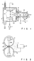
- Fig. 1 is a sectional view schematically showing the plasma etching apparatus according to a first embodiment of the present invention and Fig. 2 shows the main portion of the plasma etching apparatus enlarged.
- the processing apparatus of the present invention in which plasma is used includes a vacuum processing chamber 3 which is an Al-made box provided with a reactive gas supply pipe 1 and an exhaust pipe 2 connected to suction means 2a.
- a pair of susceptors 5 and 6 are opposed to each other to hold substrates or semiconductor wafers 4 thereon in the processing chamber 3.
- the lower susceptor 6 is connected to a high frequency power source 7 while the upper one 5 is earthed.
- the processing chamber 3 is also earthed.
- the pressure in the processing chamber 3 is set 1 x 10 ⁇ 4 - 1 x 10 ⁇ 3 Torr.
- Plasma discharge is generated between the susceptors 5 and 6 in the processing chamber 3 by the high frequency power source 7. Reactive gas supplied into the processing chamber 3 through the supply pipe 1 is thus made plasma to create plasma atmosphere in the processing chamber 3.
- An electron inlet 8 is formed at a side wall of the processing chamber 3.
- An electron supply chamber 10 is connected to the electron inlet 8 through a gate valve 9.
- a filament 11 which serves as electron generator means is arranged in the electron supply chamber 10, extending to the electron inlet 8.
- Power (of 10A and 15 - 20V, for example) is applied from an AC power source 12, located outside the electron supply chamber 10, to the filament 11 to generate thermions or thermo-electrons.
- the filament 11 may be heated by a DC power source.
- a DC power source 14 (of 20 - 30V, for example) is connected at the anode side to the electrode 13a and at the cathode side to the filament 11.
- the electrode 13a and the anode side of the DC power source 14 are earthed.
- Insulating members 16 are interposed between the electron supply chamber 10 and the processing chamber 3 and also between the electron supply chamber 10 and a filament attaching plate 15.
- the electron supply chamber 10 has an exhaust outlet 17 connected to a suction means 17a, thereby enabling the electron supply chamber 10 to be kept vacuum (10 ⁇ 1 Torr).
- low energy electrons created by the filament 11 are introduced into the processing chamber 3 along the magnetic field A caused by the coil magnet 13. These electrons thus introduced into the processing chamber 3 activate the reactive gas supplied into the processing chamber 3 through the supply pipe 1. Plasma discharge is therefore generated by high frequency current or power applied from the high frequency power source 7 across the susceptors 5 and 6.
- the semiconductor wafers 4 are etched by ions, electrons and neutral active species in the plasma thus generated.
- the introduction of electrons into the processing chamber 3 may be continuously carried out while conducting the plasma process, or it may be arranged that electrons are introduced into the processing chamber 3 at the time of operation start and plasma discharge is conducted and that the gate valve 9 is then closed to stop the supply of electrons.
- susceptors 5 and 6 have been opposed to each other in the above-described case, only the lower susceptor 6 may be used or an additional susceptor may be located on one side of the upper and lower opposed susceptors 5 and 6.
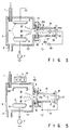
- Fig. 3 is a sectional view schematically showing the plasma etching apparatus according to a second embodiment of the present invention.
- the second plasma etching apparatus includes a different electron generator means. More specifically, the electron generator means is a gas electric discharge member 18 attached to that side of the electron supply chamber 10 which is opposed to the electron inlet 8 of the processing chamber 3.
- the gas discharge member 18 includes a Ta-made electrode 18 and an LaB6-made filament 18b.
- Inactive gas such as argon (Ar) or helium (He) is introduced from a gas supply source (not shown) into the gas discharge member 18. It is preferable to use Ar gas.
- the DC power source 14 (40V, for example) is connected between the gas discharge member 18 and the electrode 13a in the same manner as in the above-described first embodiment.
- Fig. 4 is a sectional view schematically showing the plasma etching apparatus according to a third embodiment of the present invention.
- the third plasma etching apparatus is arranged to uniformly introduce electrons generated by the electron generator means into the processing chamber. More specifically, electron inlets 8 and 8 are formed at both upper corners of the processing chamber 3 and the electron supply chamber 10 is connected to each of these electron inlets 8 and 8.
- the filament 11 which serves as the electron generator means is arranged in each of the electron supply chambers 10. Although only the lower susceptor 6 has been located in the processing chamber 3 in this case, the upper susceptor 5 may be opposed to the lower one 6 as shown by a broken line.
- the third plasma etching apparatus When the third plasma etching apparatus is arranged as described above, electrons introduced from two electron supply chambers 10 into the processing chamber 3 can be kept more uniform. This enables plasma to be generated at a higher efficiency and the semiconductor wafer or wafers 4 to be etched also at a higher efficiency.
- two electron inlets 8 and 8 have been formed at both upper corners of the processing chamber 3 and the electron supply chambers 10 have been connected to them in the third example, they may be located at any two optional positions of the processing chamber 3. Or they may be formed at three or more positions thereof.
- the filaments 11 have been used as the electron generator means in the third example, they may be replaced by the gas electric discharge members 18 used in the second example.
- Fig. 5 is a sectional view schematically showing the plasma etching apparatus according to a fourth embodiment of the present invention.
- an electron supply source is added to the processing chamber 3 of the magnetron plasma etching apparatus.
- a magnetic field generator means 19 which generates magnetic field parallel to the semiconductor wafer 4 is located on the top of the processing chamber 3. Magnetic and electric fields are generated, perpendicular to each other, on the surface of the semiconductor 4, so that magnetron discharge can be caused.
- the electron inlet 8 is formed at a side of the processing chamber 3 and the electron supply chamber 10 is connected to the electron inlet 8.
- the electron generator means (or filament) 11 is located in the electron supply chamber 10.
- a cover electrode 20 Arranged above the susceptor 6 is a cover electrode 20 which is earthed.
- magnetron plasma When magnetron plasma is used in this manner, higher density plasma can be generated under higher vacuum to achieve a finer process, as compared with the conventional magnetron plasma etching apparatus.
- the fourth embodiment may have plural electron supply chambers, as shown in the third embodiment.
- Tests were conducted to check the relation between degree of vacuum and plasma discharge in the plasma processing apparatus of the present invention.
- the second plasma etching apparatus shown in Fig. 3 was used but the processing chamber 3 had only the lower susceptor 6 in this case.
- the degree of vacuum in the processing chamber 3 was set at 4m, 1m and 0.5m Torr.
- the effective power (W) of plasma discharge was set at 0.2, 0.5, 0.7, 3.5, 8 and 10W.
- the gate valve was kept opened and closed. Chlorine gas was used as the reactive gas.
- the present invention can also be applied to those apparatuses in which the upper susceptor 5 is connected to the high frequency power source 7 while the lower one 6 is earthed. Further, the present invention can be applied to other plasma-processing apparatuses such as the plasma CVD apparatus.
Landscapes
- Engineering & Computer Science (AREA)
- Physics & Mathematics (AREA)
- Chemical & Material Sciences (AREA)
- Plasma & Fusion (AREA)
- Analytical Chemistry (AREA)
- Microelectronics & Electronic Packaging (AREA)
- General Physics & Mathematics (AREA)
- Manufacturing & Machinery (AREA)
- Computer Hardware Design (AREA)
- Toxicology (AREA)
- Power Engineering (AREA)
- Condensed Matter Physics & Semiconductors (AREA)
- Health & Medical Sciences (AREA)
- High Energy & Nuclear Physics (AREA)
- Plasma Technology (AREA)
- Drying Of Semiconductors (AREA)
- ing And Chemical Polishing (AREA)
Applications Claiming Priority (2)
| Application Number | Priority Date | Filing Date | Title |
|---|---|---|---|
| JP3122878A JPH04326725A (ja) | 1991-04-26 | 1991-04-26 | プラズマ装置 |
| JP122878/91 | 1991-04-26 |
Publications (2)
| Publication Number | Publication Date |
|---|---|
| EP0510401A1 true EP0510401A1 (fr) | 1992-10-28 |
| EP0510401B1 EP0510401B1 (fr) | 1995-11-22 |
Family
ID=14846876
Family Applications (1)
| Application Number | Title | Priority Date | Filing Date |
|---|---|---|---|
| EP92105684A Expired - Lifetime EP0510401B1 (fr) | 1991-04-26 | 1992-04-02 | Dispositif pour traitement par plasma |
Country Status (6)
| Country | Link |
|---|---|
| US (1) | US5368676A (fr) |
| EP (1) | EP0510401B1 (fr) |
| JP (1) | JPH04326725A (fr) |
| KR (1) | KR0177590B1 (fr) |
| DE (1) | DE69206187T2 (fr) |
| TW (1) | TW201854B (fr) |
Cited By (3)
| Publication number | Priority date | Publication date | Assignee | Title |
|---|---|---|---|---|
| EP0665306A1 (fr) * | 1994-01-19 | 1995-08-02 | TOKYO ELECTRON AMERICA Inc. | Procédé et dispositif d'allumage d'un plasma dans un module de traitement |
| EP0782173A2 (fr) * | 1995-10-31 | 1997-07-02 | Balzers und Leybold Deutschland Holding AG | Dispositif pour le revêtement d'un substrat utilisant un procédé de dépÔt chimique en phase vapeur |
| EP0783174A2 (fr) * | 1995-10-27 | 1997-07-09 | Balzers und Leybold Deutschland Holding AG | Dispositif pour le revêtement d'un substrat |
Families Citing this family (31)
| Publication number | Priority date | Publication date | Assignee | Title |
|---|---|---|---|---|
| US5122431A (en) * | 1988-09-14 | 1992-06-16 | Fujitsu Limited | Thin film formation apparatus |
| AU6405496A (en) * | 1995-06-29 | 1997-01-30 | Lam Research Corporation | A scalable helicon wave plasma processing device with a non-cylindrical source chamber |
| US6027663A (en) * | 1995-08-28 | 2000-02-22 | Georgia Tech Research Corporation | Method and apparatus for low energy electron enhanced etching of substrates |
| WO1997008362A1 (fr) * | 1995-08-28 | 1997-03-06 | Georgia Tech Research Corporation | Procede et dispositif d'attaque amelioree de substrats par des electrons a faible energie |
| US5882538A (en) * | 1995-08-28 | 1999-03-16 | Georgia Tech Research Corporation | Method and apparatus for low energy electron enhanced etching of substrates |
| US5917285A (en) * | 1996-07-24 | 1999-06-29 | Georgia Tech Research Corporation | Apparatus and method for reducing operating voltage in gas discharge devices |
| US6258287B1 (en) * | 1996-08-28 | 2001-07-10 | Georgia Tech Research Corporation | Method and apparatus for low energy electron enhanced etching of substrates in an AC or DC plasma environment |
| US6033587A (en) * | 1996-09-20 | 2000-03-07 | Georgia Tech Research Corporation | Method and apparatus for low energy electron enhanced etching and cleaning of substrates in the positive column of a plasma |
| KR100496809B1 (ko) * | 1997-08-26 | 2005-09-06 | 인천광역시 | 플라즈마방전에의한배가스처리장치 |
| JP4287936B2 (ja) * | 1999-02-01 | 2009-07-01 | 中外炉工業株式会社 | 真空成膜装置 |
| US7129694B2 (en) * | 2002-05-23 | 2006-10-31 | Applied Materials, Inc. | Large substrate test system |
| DE10227332A1 (de) * | 2002-06-19 | 2004-01-15 | Akt Electron Beam Technology Gmbh | Ansteuervorrichtung mit verbesserten Testeneigenschaften |
| US7032536B2 (en) * | 2002-10-11 | 2006-04-25 | Sharp Kabushiki Kaisha | Thin film formation apparatus including engagement members for support during thermal expansion |
| US7319335B2 (en) | 2004-02-12 | 2008-01-15 | Applied Materials, Inc. | Configurable prober for TFT LCD array testing |
| US20060038554A1 (en) * | 2004-02-12 | 2006-02-23 | Applied Materials, Inc. | Electron beam test system stage |
| US6833717B1 (en) * | 2004-02-12 | 2004-12-21 | Applied Materials, Inc. | Electron beam test system with integrated substrate transfer module |
| US7355418B2 (en) * | 2004-02-12 | 2008-04-08 | Applied Materials, Inc. | Configurable prober for TFT LCD array test |
| US7075323B2 (en) * | 2004-07-29 | 2006-07-11 | Applied Materials, Inc. | Large substrate test system |
| US7535238B2 (en) * | 2005-04-29 | 2009-05-19 | Applied Materials, Inc. | In-line electron beam test system |
| CN100358098C (zh) * | 2005-08-05 | 2007-12-26 | 中微半导体设备(上海)有限公司 | 半导体工艺件处理装置 |
| US7569818B2 (en) * | 2006-03-14 | 2009-08-04 | Applied Materials, Inc. | Method to reduce cross talk in a multi column e-beam test system |
| US7602199B2 (en) | 2006-05-31 | 2009-10-13 | Applied Materials, Inc. | Mini-prober for TFT-LCD testing |
| US7786742B2 (en) | 2006-05-31 | 2010-08-31 | Applied Materials, Inc. | Prober for electronic device testing on large area substrates |
| US9111728B2 (en) | 2011-04-11 | 2015-08-18 | Lam Research Corporation | E-beam enhanced decoupled source for semiconductor processing |
| US8900403B2 (en) | 2011-05-10 | 2014-12-02 | Lam Research Corporation | Semiconductor processing system having multiple decoupled plasma sources |
| US9177756B2 (en) * | 2011-04-11 | 2015-11-03 | Lam Research Corporation | E-beam enhanced decoupled source for semiconductor processing |
| US8951384B2 (en) | 2011-10-20 | 2015-02-10 | Applied Materials, Inc. | Electron beam plasma source with segmented beam dump for uniform plasma generation |
| US20130098555A1 (en) * | 2011-10-20 | 2013-04-25 | Applied Materials, Inc. | Electron beam plasma source with profiled conductive fins for uniform plasma generation |
| US9129777B2 (en) | 2011-10-20 | 2015-09-08 | Applied Materials, Inc. | Electron beam plasma source with arrayed plasma sources for uniform plasma generation |
| US9443700B2 (en) | 2013-03-12 | 2016-09-13 | Applied Materials, Inc. | Electron beam plasma source with segmented suppression electrode for uniform plasma generation |
| TWI573700B (zh) * | 2015-02-13 | 2017-03-11 | rong-gui Deng | Assembly equipment for loading equipment and its applications |
Citations (4)
| Publication number | Priority date | Publication date | Assignee | Title |
|---|---|---|---|---|
| US4175029A (en) * | 1978-03-16 | 1979-11-20 | Dmitriev Jury A | Apparatus for ion plasma coating of articles |
| EP0031704A2 (fr) * | 1979-12-26 | 1981-07-08 | Western Electric Company, Incorporated | Appareil pour le traitement par plasma réactif |
| EP0061906A1 (fr) * | 1981-03-26 | 1982-10-06 | Inoue-Japax Research Incorporated | Procédé et appareil pour l'usinage d'une pièce par particules à grande énergie et un produit usiné de cette manière |
| WO1991013458A1 (fr) * | 1990-03-02 | 1991-09-05 | Varian Associates, Inc. | Appareil de neutralisation de charge pour systeme d'implantation d'ions |
Family Cites Families (11)
| Publication number | Priority date | Publication date | Assignee | Title |
|---|---|---|---|---|
| DE2438531C3 (de) * | 1974-08-10 | 1982-04-08 | Fa. Carl Freudenberg, 6940 Weinheim | Separatorenmaterial |
| US4269137A (en) * | 1979-03-19 | 1981-05-26 | Xerox Corporation | Pretreatment of substrates prior to thin film deposition |
| JPS6010731A (ja) * | 1983-06-30 | 1985-01-19 | Fujitsu Ltd | プラズマエツチング装置 |
| CH664768A5 (de) * | 1985-06-20 | 1988-03-31 | Balzers Hochvakuum | Verfahren zur beschichtung von substraten in einer vakuumkammer. |
| DE3614398A1 (de) * | 1985-07-01 | 1987-01-08 | Balzers Hochvakuum | Anordnung zum behandeln von werkstuecken mit einer evakuierbaren kammer |
| YU46728B (sh) * | 1986-10-23 | 1994-04-05 | VUJO dr. MILJEVIĆ | Jonsko-elektronski izvor sa šupljom anodom |
| US4878995A (en) * | 1987-07-02 | 1989-11-07 | Kabushiki Kaisha Toshiba | Method of dry etching and apparatus for use in such method |
| ATE65265T1 (de) * | 1987-08-26 | 1991-08-15 | Balzers Hochvakuum | Verfahren zur aufbringung von schichten auf substraten und vakuumbeschichtungsanlage zur durchfuehrung des verfahrens. |
| JPH01270320A (ja) * | 1988-04-22 | 1989-10-27 | Seiko Epson Corp | 絶縁薄膜堆積装置 |
| JPH0752635B2 (ja) * | 1988-10-18 | 1995-06-05 | 日新電機株式会社 | イオン源装置 |
| JP2892787B2 (ja) * | 1990-07-20 | 1999-05-17 | 東京エレクトロン株式会社 | 電気信号の抽出方法 |
-
1991
- 1991-04-26 JP JP3122878A patent/JPH04326725A/ja not_active Withdrawn
-
1992
- 1992-04-01 TW TW081102492A patent/TW201854B/zh active
- 1992-04-02 DE DE69206187T patent/DE69206187T2/de not_active Expired - Lifetime
- 1992-04-02 EP EP92105684A patent/EP0510401B1/fr not_active Expired - Lifetime
- 1992-04-16 KR KR1019920006390A patent/KR0177590B1/ko not_active IP Right Cessation
-
1993
- 1993-12-09 US US08/164,874 patent/US5368676A/en not_active Expired - Lifetime
Patent Citations (4)
| Publication number | Priority date | Publication date | Assignee | Title |
|---|---|---|---|---|
| US4175029A (en) * | 1978-03-16 | 1979-11-20 | Dmitriev Jury A | Apparatus for ion plasma coating of articles |
| EP0031704A2 (fr) * | 1979-12-26 | 1981-07-08 | Western Electric Company, Incorporated | Appareil pour le traitement par plasma réactif |
| EP0061906A1 (fr) * | 1981-03-26 | 1982-10-06 | Inoue-Japax Research Incorporated | Procédé et appareil pour l'usinage d'une pièce par particules à grande énergie et un produit usiné de cette manière |
| WO1991013458A1 (fr) * | 1990-03-02 | 1991-09-05 | Varian Associates, Inc. | Appareil de neutralisation de charge pour systeme d'implantation d'ions |
Non-Patent Citations (1)
| Title |
|---|
| PATENT ABSTRACTS OF JAPAN vol. 9, no. 123 (E-317)(1846) 28 May 1985 & JP-A-60 010 731 ( FUJITSU K.K. ) 19 January 1985 * |
Cited By (8)
| Publication number | Priority date | Publication date | Assignee | Title |
|---|---|---|---|---|
| EP0665306A1 (fr) * | 1994-01-19 | 1995-08-02 | TOKYO ELECTRON AMERICA Inc. | Procédé et dispositif d'allumage d'un plasma dans un module de traitement |
| US5565036A (en) * | 1994-01-19 | 1996-10-15 | Tel America, Inc. | Apparatus and method for igniting plasma in a process module |
| US5789867A (en) * | 1994-01-19 | 1998-08-04 | Tel America, Inc. | Apparatus and method for igniting plasma in a process module |
| EP0783174A2 (fr) * | 1995-10-27 | 1997-07-09 | Balzers und Leybold Deutschland Holding AG | Dispositif pour le revêtement d'un substrat |
| EP0783174A3 (fr) * | 1995-10-27 | 1999-02-17 | Balzers und Leybold Deutschland Holding AG | Dispositif pour le revêtement d'un substrat |
| US6168698B1 (en) | 1995-10-27 | 2001-01-02 | Balzers Und Leybold Deutschland Holding Ag | Apparatus for coating a substrate |
| EP0782173A2 (fr) * | 1995-10-31 | 1997-07-02 | Balzers und Leybold Deutschland Holding AG | Dispositif pour le revêtement d'un substrat utilisant un procédé de dépÔt chimique en phase vapeur |
| EP0782173A3 (fr) * | 1995-10-31 | 1999-02-17 | Balzers und Leybold Deutschland Holding AG | Dispositif pour le revêtement d'un substrat utilisant un procédé de dépÔt chimique en phase vapeur |
Also Published As
| Publication number | Publication date |
|---|---|
| KR0177590B1 (ko) | 1999-04-15 |
| DE69206187D1 (de) | 1996-01-04 |
| TW201854B (fr) | 1993-03-11 |
| KR920020614A (ko) | 1992-11-21 |
| US5368676A (en) | 1994-11-29 |
| EP0510401B1 (fr) | 1995-11-22 |
| DE69206187T2 (de) | 1996-05-02 |
| JPH04326725A (ja) | 1992-11-16 |
Similar Documents
| Publication | Publication Date | Title |
|---|---|---|
| EP0510401A1 (fr) | Dispositif pour traitement par plasma | |
| US5304279A (en) | Radio frequency induction/multipole plasma processing tool | |
| EP0379828B1 (fr) | Dispositif de traitement par plasma multipolaire à induction de radiofréquence | |
| JP3381916B2 (ja) | 低周波誘導型高周波プラズマ反応装置 | |
| US7972467B2 (en) | Apparatus and method to confine plasma and reduce flow resistance in a plasma reactor | |
| US6213050B1 (en) | Enhanced plasma mode and computer system for plasma immersion ion implantation | |
| EP0064163B1 (fr) | Système de décapage par plasma à grande vitesse | |
| EP0271341B1 (fr) | Procédé et dispositif d'attaque par ions | |
| US6664737B1 (en) | Dielectric barrier discharge apparatus and process for treating a substrate | |
| US4873445A (en) | Source of ions of the triode type with a single high frequency exitation ionization chamber and magnetic confinement of the multipole type | |
| US6300227B1 (en) | Enhanced plasma mode and system for plasma immersion ion implantation | |
| US9564297B2 (en) | Electron beam plasma source with remote radical source | |
| US20030150562A1 (en) | Apparatus and method to control the uniformity of plasma by reducing radial loss | |
| US20180308663A1 (en) | Plasma reactor with phase shift applied across electrode array | |
| US20010002584A1 (en) | Enhanced plasma mode and system for plasma immersion ion implantation | |
| JPH10261498A (ja) | プラズマ処理装置及びプラズマ処理方法 | |
| JP2004353066A (ja) | プラズマ源およびプラズマ処理装置 | |
| US20180308664A1 (en) | Plasma reactor with filaments and rf power applied at multiple frequencies | |
| JPS6338585A (ja) | プラズマ装置 | |
| WO2018200409A1 (fr) | Application d'énergie à des électrodes d'un réacteur à plasma | |
| JP2003077904A (ja) | プラズマ処理装置及びプラズマ処理方法 | |
| JPH0774115A (ja) | プラズマ処理装置 | |
| JPH08195379A (ja) | プラズマ処理方法及びプラズマ処理装置 | |
| JPS6380534A (ja) | プラズマ処理装置 | |
| US20180308667A1 (en) | Plasma reactor with groups of electrodes |
Legal Events
| Date | Code | Title | Description |
|---|---|---|---|
| PUAI | Public reference made under article 153(3) epc to a published international application that has entered the european phase |
Free format text: ORIGINAL CODE: 0009012 |
|
| 17P | Request for examination filed |
Effective date: 19920402 |
|
| AK | Designated contracting states |
Kind code of ref document: A1 Designated state(s): DE FR GB IT NL |
|
| 17Q | First examination report despatched |
Effective date: 19940628 |
|
| GRAA | (expected) grant |
Free format text: ORIGINAL CODE: 0009210 |
|
| AK | Designated contracting states |
Kind code of ref document: B1 Designated state(s): DE FR GB IT NL |
|
| ITF | It: translation for a ep patent filed |
Owner name: BUGNION S.P.A. |
|
| ET | Fr: translation filed | ||
| REF | Corresponds to: |
Ref document number: 69206187 Country of ref document: DE Date of ref document: 19960104 |
|
| PLBE | No opposition filed within time limit |
Free format text: ORIGINAL CODE: 0009261 |
|
| STAA | Information on the status of an ep patent application or granted ep patent |
Free format text: STATUS: NO OPPOSITION FILED WITHIN TIME LIMIT |
|
| 26N | No opposition filed | ||
| PGFP | Annual fee paid to national office [announced via postgrant information from national office to epo] |
Ref country code: GB Payment date: 19980324 Year of fee payment: 7 |
|
| PGFP | Annual fee paid to national office [announced via postgrant information from national office to epo] |
Ref country code: FR Payment date: 19980408 Year of fee payment: 7 |
|
| PGFP | Annual fee paid to national office [announced via postgrant information from national office to epo] |
Ref country code: NL Payment date: 19980430 Year of fee payment: 7 |
|
| PG25 | Lapsed in a contracting state [announced via postgrant information from national office to epo] |
Ref country code: GB Free format text: LAPSE BECAUSE OF NON-PAYMENT OF DUE FEES Effective date: 19990402 |
|
| PG25 | Lapsed in a contracting state [announced via postgrant information from national office to epo] |
Ref country code: NL Free format text: LAPSE BECAUSE OF NON-PAYMENT OF DUE FEES Effective date: 19991101 |
|
| GBPC | Gb: european patent ceased through non-payment of renewal fee |
Effective date: 19990402 |
|
| PG25 | Lapsed in a contracting state [announced via postgrant information from national office to epo] |
Ref country code: FR Free format text: LAPSE BECAUSE OF NON-PAYMENT OF DUE FEES Effective date: 19991231 |
|
| NLV4 | Nl: lapsed or anulled due to non-payment of the annual fee |
Effective date: 19991101 |
|
| REG | Reference to a national code |
Ref country code: FR Ref legal event code: ST |
|
| PG25 | Lapsed in a contracting state [announced via postgrant information from national office to epo] |
Ref country code: IT Free format text: LAPSE BECAUSE OF NON-PAYMENT OF DUE FEES;WARNING: LAPSES OF ITALIAN PATENTS WITH EFFECTIVE DATE BEFORE 2007 MAY HAVE OCCURRED AT ANY TIME BEFORE 2007. THE CORRECT EFFECTIVE DATE MAY BE DIFFERENT FROM THE ONE RECORDED. Effective date: 20050402 |
|
| PGFP | Annual fee paid to national office [announced via postgrant information from national office to epo] |
Ref country code: DE Payment date: 20110330 Year of fee payment: 20 |
|
| REG | Reference to a national code |
Ref country code: DE Ref legal event code: R071 Ref document number: 69206187 Country of ref document: DE |
|
| REG | Reference to a national code |
Ref country code: DE Ref legal event code: R071 Ref document number: 69206187 Country of ref document: DE |
|
| PG25 | Lapsed in a contracting state [announced via postgrant information from national office to epo] |
Ref country code: DE Free format text: LAPSE BECAUSE OF EXPIRATION OF PROTECTION Effective date: 20120403 |