EP0507213A2 - Lichtsender - Google Patents
Lichtsender Download PDFInfo
- Publication number
- EP0507213A2 EP0507213A2 EP92105217A EP92105217A EP0507213A2 EP 0507213 A2 EP0507213 A2 EP 0507213A2 EP 92105217 A EP92105217 A EP 92105217A EP 92105217 A EP92105217 A EP 92105217A EP 0507213 A2 EP0507213 A2 EP 0507213A2
- Authority
- EP
- European Patent Office
- Prior art keywords
- current
- light
- circuit
- modulation
- voltage conversion
- Prior art date
- Legal status (The legal status is an assumption and is not a legal conclusion. Google has not performed a legal analysis and makes no representation as to the accuracy of the status listed.)
- Granted
Links
Images


Classifications
-
- H—ELECTRICITY
- H04—ELECTRIC COMMUNICATION TECHNIQUE
- H04B—TRANSMISSION
- H04B10/00—Transmission systems employing electromagnetic waves other than radio-waves, e.g. infrared, visible or ultraviolet light, or employing corpuscular radiation, e.g. quantum communication
- H04B10/50—Transmitters
- H04B10/501—Structural aspects
- H04B10/503—Laser transmitters
- H04B10/504—Laser transmitters using direct modulation
-
- H—ELECTRICITY
- H04—ELECTRIC COMMUNICATION TECHNIQUE
- H04B—TRANSMISSION
- H04B10/00—Transmission systems employing electromagnetic waves other than radio-waves, e.g. infrared, visible or ultraviolet light, or employing corpuscular radiation, e.g. quantum communication
- H04B10/50—Transmitters
- H04B10/564—Power control
-
- H—ELECTRICITY
- H01—ELECTRIC ELEMENTS
- H01S—DEVICES USING THE PROCESS OF LIGHT AMPLIFICATION BY STIMULATED EMISSION OF RADIATION [LASER] TO AMPLIFY OR GENERATE LIGHT; DEVICES USING STIMULATED EMISSION OF ELECTROMAGNETIC RADIATION IN WAVE RANGES OTHER THAN OPTICAL
- H01S5/00—Semiconductor lasers
- H01S5/06—Arrangements for controlling the laser output parameters, e.g. by operating on the active medium
- H01S5/068—Stabilisation of laser output parameters
- H01S5/0683—Stabilisation of laser output parameters by monitoring the optical output parameters
- H01S5/06832—Stabilising during amplitude modulation
Definitions
- the invention relates to a light transmitter for preventing the degradation of the extinction ratio of light signal and the occurrence of pulse width distortion.
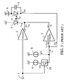
- FIG. 3 is a block diagram of the prior transmitter disclosed in Japanese Patent publication 2-44420/1990.
- 1 is a transmitting data input terminal.
- 2 is a modulator connected to the transmitting data input terminal 1.
- 3 is a laser diode.
- 4 is a light receiving element for receiving a part of the output light from the laser diode 3.
- 5 is a capacitor connected in parallel to the light receiving element 4.
- 6 is a bias voltage source for supplying the voltage to the light receiving element 4.
- 7 is a current amplifier.
- 8 is a first reference current source.
- 9 is a second reference current source.
- 10 is a switching circuit connected to the output terminal of the second current source 9 for switching the second current source in response to the binary transmitted data.
- the output current from the reference current source 9 is added to the second output current by the switching circuit 10 in response to the binary transmitted data.
- the relation between the currents l O1 outputted from the first current source, 1 02 outputted from the second current source and the reference current 1 0 is obtained as follows.
- the output light of the laser diode 3 is radiated to the light receiving element 4.
- the current IpD flowing the light receiving element 4 is in proportion to the output light of the laser diode as shown in the following equation.
- the current difference (l o - Ip D ) between the synthesized current l o and the current IpD flowing in the light receiving element 4 is amplified by the current amplifier 7 and applied to the laser diode 3.
- the current IpD flowing in the light receiving element 4 is averaged in the capacitor 5 connected in parallel to the light receiving 4.
- the current I B applied to the laser diode 3 is obtained as follows.
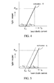
- the current to light conversion characteristics of the laser diode 3 is shown in FIG. 4. From the FIG. 4, the peak value Pout of the light output of the laser diode is obtained in the following equation. where,
- the equations from (1) to (4) shows that the bias current I B is controlled so that the peak value of the light output Pout may be constant if the threshold current I th varies by some reasons. That is, if I th increases to I th ', the bias current I B is controlled automatically to increases to I B ' in order to maintain the constant light output by the current amplifier as shown in FIG.5.
- I B is set as follows as shown in FIGs. 4,5 and 7.
- I B changes as follows.
- a light transmitter comprising a first current to voltage conversion circuit for converting the signal current flowing in the light receiving element to a voltage signal, a second current to voltage conversion circuit for converting the modulation current outputted from the modulator to a voltage signal and a mismatch detection circuit for detecting the mismatch between the current outputted from the first current to voltage conversion circuit and the current outputted from the second current to voltage conversion circuit, and a modulation current control circuit for limiting the modulation current by the detected output voltage.
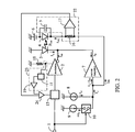
- FIG. 1 is a circuit diagram of a first embodiment the present invention.
- 11 is a filter for averaging the current flowing in the light receiving element 4.
- 12 is a first current to voltage conversion circuit.
- 13 is a second current to voltage conversion circuit.
- 14 is a mismatch detection circuit for detecting the mismatch between the output of the first current to voltage conversion circuit 12 and the output of the second current to voltage conversion circuit 13.
- 15 is a modulation current control circuit for controlling the modulation current by the output current of the mismatch detection circuit 14.
- 16 is first current to voltage conversion resistor in the first current to voltage conversion circuit 12.
- 17 is an amplifier for amplifying the output of the first current to voltage conversion resistor.
- 18 is second current to voltage conversion resistor in the second current to voltage conversion circuit 13.
- 19 is a second amplifier for amplifying the output of the second current to voltage conversion resistor.
- Other elements of the first embodiment are the same as those having the same numerals in FIG. 3, and therefore the detailed descriptions are omitted.
- the circuit operates in the same manner as that of the conventional circuit for controlling the light output Pout to be constant.
- the difference from the conventional circuit is in that the first embodiment uses a filter 11 for averaging current IpD flowing in the light receiving element 4.
- the filter 11 is supplied to convert the current IpD to a voltage signal without being averaged.
- the second current to voltage converter 13 equivalently converts the inverted modulated current to a voltage signal.
- the output voltages of the first current to voltage conversion circuit 12 and the second current to voltage conversion circuit 13 are applied to the mismatch detection circuit 14.
- the mismatch detection circuit 14 detects the mismatch of the pulse width of the two voltage output signals.
- the laser diode has a characteristic in connection with the modulation current and the output light as shown in FIG. 6.
- the rise time of the output light lags from the modulation current and then the pulse width of the light output becomes narrower at the condition of the equation (8).
- the mismatch detection signal is outputted from the mismatch detection circuit 14.
- the bias current I B ' decreases, because (l o p + I B ') must be constant in order to maintain a constant light output Pout.
- the modulation current l o p becomes equal to l o p', the bias current becomes I B and the formula (6) is satisfied. Therefore the system is stabilized.
- FIG. 2 is a circuit diagram of a second embodiment the present invention.
- 11 is a filter for averaging the modulated current outputted from the modulator.
- 22 is a first current to voltage conversion and averaging circuit.
- 23 is a second current to voltage conversion and averaging circuit.
- 24 is a comparison circuit for comparing the outputs between the output of the first current to voltage conversion and averaging circuit 22 and the output of the second current to voltage conversion and averaging circuit 23.
- 15 is a modulation current control circuit for controlling the modulation current by the output signal of the comparison circuit 24.
- 16 is first current to voltage conversion resistor in the first current to voltage conversion and averaging circuit 22.
- 17 is an amplifier for amplifying the output of the first current to voltage conversion resistor 16.
- the circuit operates in the same manner as that of the conventional circuit for controlling the light output Pout to be constant.
- the difference from the conventional circuit is in that the second embodiment uses the filter 11 for averaging the voltage converted by the second resistor 18 from the modulation current l o p outputted from the modulator 2.
- the first current to voltage conversion and averaging circuit 22 converts the current IpD flowing in the light receiving element 4 to a voltage signal.
- the current flowing in the light receiving element 4 is averaged by the capacitor 5 connected to the diode 4 as shown in FIG. 2.
- the output voltages of the first current to voltage conversion and averaging circuit 22 and the second current to voltage conversion and averaging circuit 23 are applied to the comparison circuit 24.
- the comparison circuit 24 compares the two voltage signals and outputs a control signal for limiting to increase the modulation current l o p if the output of the second current to voltage conversion and averaging circuit 23 is greater than the output of the first current to voltage conversion and averaging circuit 22.
- the laser diode has a characteristic as shown in FIG. 6 in connection with the modulation current and the output light.
- FIG. 6 when the rise time of the light output lags the modulation current, then the pulse width of the light output becomes narrower and the averaged level decreases at the condition of the equation (8).
- the bias current I B ' decreases, because (l o p + I B ') must be constant in order to maintain a constant light output Pout.
- the modulation current l o p becomes equal to l o p', the bias current becomes I B and the equation (6) is satisfied. Therefore the system is stabilized.
Landscapes
- Physics & Mathematics (AREA)
- Electromagnetism (AREA)
- Engineering & Computer Science (AREA)
- Computer Networks & Wireless Communication (AREA)
- Signal Processing (AREA)
- Optics & Photonics (AREA)
- Semiconductor Lasers (AREA)
- Optical Communication System (AREA)
Applications Claiming Priority (4)
| Application Number | Priority Date | Filing Date | Title |
|---|---|---|---|
| JP71646/91 | 1991-04-04 | ||
| JP7164691 | 1991-04-04 | ||
| JP79781/91 | 1991-04-12 | ||
| JP7978191 | 1991-04-12 |
Publications (3)
| Publication Number | Publication Date |
|---|---|
| EP0507213A2 true EP0507213A2 (de) | 1992-10-07 |
| EP0507213A3 EP0507213A3 (en) | 1993-05-05 |
| EP0507213B1 EP0507213B1 (de) | 1997-09-24 |
Family
ID=26412756
Family Applications (1)
| Application Number | Title | Priority Date | Filing Date |
|---|---|---|---|
| EP92105217A Expired - Lifetime EP0507213B1 (de) | 1991-04-04 | 1992-03-26 | Lichtsender |
Country Status (3)
| Country | Link |
|---|---|
| US (1) | US5309269A (de) |
| EP (1) | EP0507213B1 (de) |
| DE (1) | DE69222342T2 (de) |
Cited By (5)
| Publication number | Priority date | Publication date | Assignee | Title |
|---|---|---|---|---|
| EP0682391A1 (de) * | 1994-05-11 | 1995-11-15 | Alcatel N.V. | Lasermodulationsregler unter Verwendung eines Additions- und eines Amplitudenmodulationssteuerungstones |
| EP0682392A1 (de) * | 1994-05-11 | 1995-11-15 | Alcatel N.V. | Lasermodulationsregler unter Verwendung einer elektrischen NRZ-Modulationsaussteuerungsregelung |
| EP1289175A1 (de) * | 2001-09-03 | 2003-03-05 | Agilent Technologies, Inc. (a Delaware corporation) | Steuerschaltung zur Kontrolle des Extinktionsverhältnis eines Halbleiterlasers |
| US6778784B1 (en) | 1999-06-22 | 2004-08-17 | Infineon Technologies Ag | Optical transmission device |
| CN113708212A (zh) * | 2021-10-28 | 2021-11-26 | 成都明夷电子科技有限公司 | 一种基于apc和aer环路电学测量电路的测试方法 |
Families Citing this family (13)
| Publication number | Priority date | Publication date | Assignee | Title |
|---|---|---|---|---|
| JP3248155B2 (ja) * | 1991-12-26 | 2002-01-21 | 富士通株式会社 | 半導体レーザの駆動方法 |
| DE4316811A1 (de) * | 1993-05-19 | 1994-11-24 | Philips Patentverwaltung | Optisches Übertragungssystem mit einer Laserdiode |
| JPH07174629A (ja) * | 1993-12-20 | 1995-07-14 | Mitsubishi Electric Corp | 光劣化検出回路 |
| US5404367A (en) * | 1994-07-05 | 1995-04-04 | Xerox Corporation | Scanner droop and cross talk correction |
| WO1996009699A2 (en) * | 1994-09-23 | 1996-03-28 | Philips Electronics N.V. | Optical unit for restoring a pulse pattern, and receiver suitable for use in a transmission system comprising such a unit |
| US5754577A (en) * | 1996-07-23 | 1998-05-19 | Broadband Communications Products, Inc. | Compensation for variations in temperature and aging of laser diode by use of small signal, square-law portion of transfer function of diode detection circuit |
| US6822987B2 (en) * | 2000-11-22 | 2004-11-23 | Optical Communication Products, Inc. | High-speed laser array driver |
| EP1282207A4 (de) * | 2001-02-23 | 2006-08-09 | Fujitsu Ltd | Lichtsender |
| US6917639B2 (en) * | 2001-08-09 | 2005-07-12 | Ricoh Company, Ltd. | Laser driver circuit |
| JP2003218460A (ja) * | 2002-01-24 | 2003-07-31 | Sumitomo Electric Ind Ltd | レーザダイオード制御回路、およびレーザダイオードを制御する方法 |
| US6819480B2 (en) * | 2002-05-02 | 2004-11-16 | Lucent Technologies Inc. | Method and apparatus for controlling the extinction ratio of transmitters |
| JP4217490B2 (ja) * | 2003-01-17 | 2009-02-04 | 株式会社リコー | 半導体レーザ駆動装置、光書き込み装置、画像形成装置及び半導体レーザ駆動方法 |
| TWI830307B (zh) * | 2022-07-27 | 2024-01-21 | 茂達電子股份有限公司 | 具有減少控制複雜度機制的光感測器 |
Family Cites Families (9)
| Publication number | Priority date | Publication date | Assignee | Title |
|---|---|---|---|---|
| US4277846A (en) * | 1979-12-27 | 1981-07-07 | Bell Telephone Laboratories, Incorporated | Circuit for stabilizing the output of an injection laser |
| JPS59146457A (ja) * | 1983-02-10 | 1984-08-22 | Olympus Optical Co Ltd | 光出力自動制御装置 |
| DE3333247A1 (de) * | 1983-09-14 | 1985-03-28 | Siemens Ag | Optisches uebertragungssystem mit laserregelung |
| JPS60244420A (ja) * | 1984-05-17 | 1985-12-04 | Matsushita Electric Ind Co Ltd | 流体軸受グル−プ成形方法 |
| NZ218022A (en) * | 1985-10-22 | 1991-01-29 | Fujitsu Ltd | Compensated regulation of light output from semiconductor laser |
| DE3706572A1 (de) * | 1987-02-28 | 1988-09-08 | Philips Patentverwaltung | Regelung von laserdioden |
| US4796266A (en) * | 1987-12-21 | 1989-01-03 | Bell Communications Research, Inc. | Laser driver circuit with dynamic bias |
| JPH0831649B2 (ja) * | 1988-04-08 | 1996-03-27 | 日本電信電話株式会社 | レーザダイオード駆動回路 |
| US5077619A (en) * | 1989-10-25 | 1991-12-31 | Tacan Corporation | High linearity optical transmitter |
-
1992
- 1992-03-25 US US07/857,173 patent/US5309269A/en not_active Expired - Fee Related
- 1992-03-26 DE DE69222342T patent/DE69222342T2/de not_active Expired - Fee Related
- 1992-03-26 EP EP92105217A patent/EP0507213B1/de not_active Expired - Lifetime
Cited By (7)
| Publication number | Priority date | Publication date | Assignee | Title |
|---|---|---|---|---|
| EP0682391A1 (de) * | 1994-05-11 | 1995-11-15 | Alcatel N.V. | Lasermodulationsregler unter Verwendung eines Additions- und eines Amplitudenmodulationssteuerungstones |
| EP0682392A1 (de) * | 1994-05-11 | 1995-11-15 | Alcatel N.V. | Lasermodulationsregler unter Verwendung einer elektrischen NRZ-Modulationsaussteuerungsregelung |
| US6778784B1 (en) | 1999-06-22 | 2004-08-17 | Infineon Technologies Ag | Optical transmission device |
| DE19929571B4 (de) * | 1999-06-22 | 2016-01-07 | Avago Technologies General Ip (Singapore) Pte. Ltd. | Optische Sendeeinrichtung |
| EP1289175A1 (de) * | 2001-09-03 | 2003-03-05 | Agilent Technologies, Inc. (a Delaware corporation) | Steuerschaltung zur Kontrolle des Extinktionsverhältnis eines Halbleiterlasers |
| US6829267B2 (en) | 2001-09-03 | 2004-12-07 | Agilent Technologies Inc. | Control loop circuit and method therefor |
| CN113708212A (zh) * | 2021-10-28 | 2021-11-26 | 成都明夷电子科技有限公司 | 一种基于apc和aer环路电学测量电路的测试方法 |
Also Published As
| Publication number | Publication date |
|---|---|
| EP0507213A3 (en) | 1993-05-05 |
| DE69222342T2 (de) | 1998-01-29 |
| US5309269A (en) | 1994-05-03 |
| DE69222342D1 (de) | 1997-10-30 |
| EP0507213B1 (de) | 1997-09-24 |
Similar Documents
| Publication | Publication Date | Title |
|---|---|---|
| EP0507213B1 (de) | Lichtsender | |
| EP0513002B1 (de) | Lasersteuerschaltung | |
| US4612671A (en) | Laser transmitter | |
| US6301486B1 (en) | Radio telephone apparatus | |
| US5850409A (en) | Laser modulation control method and apparatus | |
| US5311005A (en) | Optical transmitters | |
| EP0930678B1 (de) | Optischer Sender | |
| JPH09238037A (ja) | 出力電力制御回路 | |
| US6486738B2 (en) | Device for controlling power in power amplifier of a portable wireless terminal | |
| US6901222B2 (en) | Optical transmission system and terminal device applicable to the system | |
| US20020057480A1 (en) | Optical receiver for optical communications | |
| JPS608640B2 (ja) | 非直線閾値装置の駆動方法および装置 | |
| US5557445A (en) | Optical signal transmitter having an apc circuit with automatic bias current control | |
| JP2000089178A (ja) | 光送信方法及びその装置 | |
| JP2005057216A (ja) | レーザダイオード駆動回路及び光送信装置 | |
| JP3024246B2 (ja) | 変調度安定化回路 | |
| JP2601097B2 (ja) | 光送信器 | |
| JPH04142127A (ja) | 光送信装置 | |
| JPH06132589A (ja) | 光送信回路 | |
| JPH05218552A (ja) | 光送信器 | |
| JPH04293329A (ja) | 光送信回路 | |
| JPH03106134A (ja) | 光送信回路 | |
| JPH06244800A (ja) | 光送信器 | |
| JPH0221182B2 (de) | ||
| JPH02205087A (ja) | 半導体レーザ制御装置 |
Legal Events
| Date | Code | Title | Description |
|---|---|---|---|
| PUAI | Public reference made under article 153(3) epc to a published international application that has entered the european phase |
Free format text: ORIGINAL CODE: 0009012 |
|
| AK | Designated contracting states |
Kind code of ref document: A2 Designated state(s): DE FR GB IT |
|
| PUAL | Search report despatched |
Free format text: ORIGINAL CODE: 0009013 |
|
| AK | Designated contracting states |
Kind code of ref document: A3 Designated state(s): DE FR GB IT |
|
| 17P | Request for examination filed |
Effective date: 19930714 |
|
| 17Q | First examination report despatched |
Effective date: 19960215 |
|
| GRAG | Despatch of communication of intention to grant |
Free format text: ORIGINAL CODE: EPIDOS AGRA |
|
| GRAH | Despatch of communication of intention to grant a patent |
Free format text: ORIGINAL CODE: EPIDOS IGRA |
|
| GRAH | Despatch of communication of intention to grant a patent |
Free format text: ORIGINAL CODE: EPIDOS IGRA |
|
| GRAA | (expected) grant |
Free format text: ORIGINAL CODE: 0009210 |
|
| AK | Designated contracting states |
Kind code of ref document: B1 Designated state(s): DE FR GB IT |
|
| ITF | It: translation for a ep patent filed | ||
| REF | Corresponds to: |
Ref document number: 69222342 Country of ref document: DE Date of ref document: 19971030 |
|
| ET | Fr: translation filed | ||
| PGFP | Annual fee paid to national office [announced via postgrant information from national office to epo] |
Ref country code: FR Payment date: 19980310 Year of fee payment: 7 |
|
| PGFP | Annual fee paid to national office [announced via postgrant information from national office to epo] |
Ref country code: GB Payment date: 19980317 Year of fee payment: 7 |
|
| PGFP | Annual fee paid to national office [announced via postgrant information from national office to epo] |
Ref country code: DE Payment date: 19980403 Year of fee payment: 7 |
|
| PLBE | No opposition filed within time limit |
Free format text: ORIGINAL CODE: 0009261 |
|
| STAA | Information on the status of an ep patent application or granted ep patent |
Free format text: STATUS: NO OPPOSITION FILED WITHIN TIME LIMIT |
|
| 26N | No opposition filed | ||
| PG25 | Lapsed in a contracting state [announced via postgrant information from national office to epo] |
Ref country code: GB Free format text: LAPSE BECAUSE OF NON-PAYMENT OF DUE FEES Effective date: 19990326 |
|
| GBPC | Gb: european patent ceased through non-payment of renewal fee |
Effective date: 19990326 |
|
| PG25 | Lapsed in a contracting state [announced via postgrant information from national office to epo] |
Ref country code: FR Free format text: LAPSE BECAUSE OF NON-PAYMENT OF DUE FEES Effective date: 19991130 |
|
| REG | Reference to a national code |
Ref country code: FR Ref legal event code: ST |
|
| PG25 | Lapsed in a contracting state [announced via postgrant information from national office to epo] |
Ref country code: DE Free format text: LAPSE BECAUSE OF NON-PAYMENT OF DUE FEES Effective date: 20000101 |
|
| PG25 | Lapsed in a contracting state [announced via postgrant information from national office to epo] |
Ref country code: IT Free format text: LAPSE BECAUSE OF NON-PAYMENT OF DUE FEES Effective date: 20050326 |