EP0505253A2 - Appareil de réproduction d'information à partir d'un disque magnéto-optique - Google Patents
Appareil de réproduction d'information à partir d'un disque magnéto-optique Download PDFInfo
- Publication number
- EP0505253A2 EP0505253A2 EP92400687A EP92400687A EP0505253A2 EP 0505253 A2 EP0505253 A2 EP 0505253A2 EP 92400687 A EP92400687 A EP 92400687A EP 92400687 A EP92400687 A EP 92400687A EP 0505253 A2 EP0505253 A2 EP 0505253A2
- Authority
- EP
- European Patent Office
- Prior art keywords
- edge detection
- read out
- signal
- leading
- delay
- Prior art date
- Legal status (The legal status is an assumption and is not a legal conclusion. Google has not performed a legal analysis and makes no representation as to the accuracy of the status listed.)
- Granted
Links
Images


Classifications
-
- G—PHYSICS
- G11—INFORMATION STORAGE
- G11B—INFORMATION STORAGE BASED ON RELATIVE MOVEMENT BETWEEN RECORD CARRIER AND TRANSDUCER
- G11B7/00—Recording or reproducing by optical means, e.g. recording using a thermal beam of optical radiation by modifying optical properties or the physical structure, reproducing using an optical beam at lower power by sensing optical properties; Record carriers therefor
-
- G—PHYSICS
- G11—INFORMATION STORAGE
- G11B—INFORMATION STORAGE BASED ON RELATIVE MOVEMENT BETWEEN RECORD CARRIER AND TRANSDUCER
- G11B20/00—Signal processing not specific to the method of recording or reproducing; Circuits therefor
- G11B20/10—Digital recording or reproducing
- G11B20/10009—Improvement or modification of read or write signals
- G11B20/10222—Improvement or modification of read or write signals clock-related aspects, e.g. phase or frequency adjustment or bit synchronisation
-
- G—PHYSICS
- G11—INFORMATION STORAGE
- G11B—INFORMATION STORAGE BASED ON RELATIVE MOVEMENT BETWEEN RECORD CARRIER AND TRANSDUCER
- G11B11/00—Recording on or reproducing from the same record carrier wherein for these two operations the methods are covered by different main groups of groups G11B3/00 - G11B7/00 or by different subgroups of group G11B9/00; Record carriers therefor
- G11B11/10—Recording on or reproducing from the same record carrier wherein for these two operations the methods are covered by different main groups of groups G11B3/00 - G11B7/00 or by different subgroups of group G11B9/00; Record carriers therefor using recording by magnetic means or other means for magnetisation or demagnetisation of a record carrier, e.g. light induced spin magnetisation; Demagnetisation by thermal or stress means in the presence or not of an orienting magnetic field
- G11B11/105—Recording on or reproducing from the same record carrier wherein for these two operations the methods are covered by different main groups of groups G11B3/00 - G11B7/00 or by different subgroups of group G11B9/00; Record carriers therefor using recording by magnetic means or other means for magnetisation or demagnetisation of a record carrier, e.g. light induced spin magnetisation; Demagnetisation by thermal or stress means in the presence or not of an orienting magnetic field using a beam of light or a magnetic field for recording by change of magnetisation and a beam of light for reproducing, i.e. magneto-optical, e.g. light-induced thermomagnetic recording, spin magnetisation recording, Kerr or Faraday effect reproducing
- G11B11/10502—Recording on or reproducing from the same record carrier wherein for these two operations the methods are covered by different main groups of groups G11B3/00 - G11B7/00 or by different subgroups of group G11B9/00; Record carriers therefor using recording by magnetic means or other means for magnetisation or demagnetisation of a record carrier, e.g. light induced spin magnetisation; Demagnetisation by thermal or stress means in the presence or not of an orienting magnetic field using a beam of light or a magnetic field for recording by change of magnetisation and a beam of light for reproducing, i.e. magneto-optical, e.g. light-induced thermomagnetic recording, spin magnetisation recording, Kerr or Faraday effect reproducing characterised by the transducing operation to be executed
- G11B11/10515—Reproducing
-
- G—PHYSICS
- G11—INFORMATION STORAGE
- G11B—INFORMATION STORAGE BASED ON RELATIVE MOVEMENT BETWEEN RECORD CARRIER AND TRANSDUCER
- G11B11/00—Recording on or reproducing from the same record carrier wherein for these two operations the methods are covered by different main groups of groups G11B3/00 - G11B7/00 or by different subgroups of group G11B9/00; Record carriers therefor
- G11B11/10—Recording on or reproducing from the same record carrier wherein for these two operations the methods are covered by different main groups of groups G11B3/00 - G11B7/00 or by different subgroups of group G11B9/00; Record carriers therefor using recording by magnetic means or other means for magnetisation or demagnetisation of a record carrier, e.g. light induced spin magnetisation; Demagnetisation by thermal or stress means in the presence or not of an orienting magnetic field
- G11B11/105—Recording on or reproducing from the same record carrier wherein for these two operations the methods are covered by different main groups of groups G11B3/00 - G11B7/00 or by different subgroups of group G11B9/00; Record carriers therefor using recording by magnetic means or other means for magnetisation or demagnetisation of a record carrier, e.g. light induced spin magnetisation; Demagnetisation by thermal or stress means in the presence or not of an orienting magnetic field using a beam of light or a magnetic field for recording by change of magnetisation and a beam of light for reproducing, i.e. magneto-optical, e.g. light-induced thermomagnetic recording, spin magnetisation recording, Kerr or Faraday effect reproducing
- G11B11/10502—Recording on or reproducing from the same record carrier wherein for these two operations the methods are covered by different main groups of groups G11B3/00 - G11B7/00 or by different subgroups of group G11B9/00; Record carriers therefor using recording by magnetic means or other means for magnetisation or demagnetisation of a record carrier, e.g. light induced spin magnetisation; Demagnetisation by thermal or stress means in the presence or not of an orienting magnetic field using a beam of light or a magnetic field for recording by change of magnetisation and a beam of light for reproducing, i.e. magneto-optical, e.g. light-induced thermomagnetic recording, spin magnetisation recording, Kerr or Faraday effect reproducing characterised by the transducing operation to be executed
- G11B11/1053—Recording on or reproducing from the same record carrier wherein for these two operations the methods are covered by different main groups of groups G11B3/00 - G11B7/00 or by different subgroups of group G11B9/00; Record carriers therefor using recording by magnetic means or other means for magnetisation or demagnetisation of a record carrier, e.g. light induced spin magnetisation; Demagnetisation by thermal or stress means in the presence or not of an orienting magnetic field using a beam of light or a magnetic field for recording by change of magnetisation and a beam of light for reproducing, i.e. magneto-optical, e.g. light-induced thermomagnetic recording, spin magnetisation recording, Kerr or Faraday effect reproducing characterised by the transducing operation to be executed to compensate for the magnetic domain drift or time shift
-
- G—PHYSICS
- G11—INFORMATION STORAGE
- G11B—INFORMATION STORAGE BASED ON RELATIVE MOVEMENT BETWEEN RECORD CARRIER AND TRANSDUCER
- G11B11/00—Recording on or reproducing from the same record carrier wherein for these two operations the methods are covered by different main groups of groups G11B3/00 - G11B7/00 or by different subgroups of group G11B9/00; Record carriers therefor
- G11B11/10—Recording on or reproducing from the same record carrier wherein for these two operations the methods are covered by different main groups of groups G11B3/00 - G11B7/00 or by different subgroups of group G11B9/00; Record carriers therefor using recording by magnetic means or other means for magnetisation or demagnetisation of a record carrier, e.g. light induced spin magnetisation; Demagnetisation by thermal or stress means in the presence or not of an orienting magnetic field
- G11B11/105—Recording on or reproducing from the same record carrier wherein for these two operations the methods are covered by different main groups of groups G11B3/00 - G11B7/00 or by different subgroups of group G11B9/00; Record carriers therefor using recording by magnetic means or other means for magnetisation or demagnetisation of a record carrier, e.g. light induced spin magnetisation; Demagnetisation by thermal or stress means in the presence or not of an orienting magnetic field using a beam of light or a magnetic field for recording by change of magnetisation and a beam of light for reproducing, i.e. magneto-optical, e.g. light-induced thermomagnetic recording, spin magnetisation recording, Kerr or Faraday effect reproducing
- G11B11/10595—Control of operating function
- G11B11/10597—Adaptations for transducing various formats on the same or different carriers
-
- G—PHYSICS
- G11—INFORMATION STORAGE
- G11B—INFORMATION STORAGE BASED ON RELATIVE MOVEMENT BETWEEN RECORD CARRIER AND TRANSDUCER
- G11B20/00—Signal processing not specific to the method of recording or reproducing; Circuits therefor
- G11B20/10—Digital recording or reproducing
- G11B20/10009—Improvement or modification of read or write signals
-
- G—PHYSICS
- G11—INFORMATION STORAGE
- G11B—INFORMATION STORAGE BASED ON RELATIVE MOVEMENT BETWEEN RECORD CARRIER AND TRANSDUCER
- G11B20/00—Signal processing not specific to the method of recording or reproducing; Circuits therefor
- G11B20/10—Digital recording or reproducing
- G11B20/12—Formatting, e.g. arrangement of data block or words on the record carriers
- G11B20/1217—Formatting, e.g. arrangement of data block or words on the record carriers on discs
-
- G—PHYSICS
- G11—INFORMATION STORAGE
- G11B—INFORMATION STORAGE BASED ON RELATIVE MOVEMENT BETWEEN RECORD CARRIER AND TRANSDUCER
- G11B20/00—Signal processing not specific to the method of recording or reproducing; Circuits therefor
- G11B20/10—Digital recording or reproducing
- G11B20/14—Digital recording or reproducing using self-clocking codes
- G11B20/1403—Digital recording or reproducing using self-clocking codes characterised by the use of two levels
- G11B20/1423—Code representation depending on subsequent bits, e.g. delay modulation, double density code, Miller code
- G11B20/1426—Code representation depending on subsequent bits, e.g. delay modulation, double density code, Miller code conversion to or from block codes or representations thereof
-
- G—PHYSICS
- G11—INFORMATION STORAGE
- G11B—INFORMATION STORAGE BASED ON RELATIVE MOVEMENT BETWEEN RECORD CARRIER AND TRANSDUCER
- G11B2220/00—Record carriers by type
- G11B2220/20—Disc-shaped record carriers
- G11B2220/25—Disc-shaped record carriers characterised in that the disc is based on a specific recording technology
- G11B2220/2525—Magneto-optical [MO] discs
Definitions
- the present invention generally relates to information read out apparatuses, and more particularly to a read out apparatus for reading out information from a magneto-optic disk.
- Magneto-optic disks are becoming popular because of the large memory capacity, high reliability and the like. Hence, the magneto-optic disk is applicable to various fields including recording and read out of image information and recording codes for use in computers.
- FIGS.1A and 1B A description will be given of the basic principle of recording and reading out information on and or from a magneto-optic disk, by referring to FIGS.1A and 1B.
- an external magnetic field of a magnet 11 is applied on a magneto-optic disk 10, and an erasing beam 12 is irradiated on a part where information is to be rewritten.
- the part which is irradiated by the erasing beam 12 is heated, and the direction of magnetization at this part is arranged in one direction.
- FIG.1B the direction of the external magnetic field of the magnet 11 is reversed.
- a recording light beam 13 is irradiated on the magneto-optic disk 10 depending on a recording data Dw shown in FIG.2(A) which is to be recorded as shown in FIG.2(B).
- the magneto-optic disk 10 is selectively heated and magnetic domains D having different directions of magnetization are formed so that intervals of edge positions of the magnetic domains correspond to the recording data Dw as shown in FIG.2(C).
- the magnetic domains D are formed on tracks or track turns of the magneto-optic disk 10.
- the mark position method forms the magnetic domains D in correspondence with the data "1"s of the recording data Dw.
- the edge recording method (or the mark length recording method) forms the magnetic domains D so that leading or trailing edges correspond to the data "1"s of the recording data Dw.
- the edge recording method is a compression technique which makes the data "1"s of the recording data Dw correspond to the edges of the magnetic domains D, and it is possible to greatly improve the recording density.
- FIG.2(A) through (C) respectively show the recording data Dw, the light emitting pattern of the recording light beam 13 and the recorded magnetic domains D on the magneto-optic disk 10 for the case where the edge recording method is employed.
- the recording light beam 13 is turned ON and OFF as shown in FIG.2(B) depending on the data "1"s of the recording data Dw shown in FIG.2(A), so that the edges of the magnetic domains D on the magneto-optic disk 10 correspond to the data "1"s of the recording data Dw as shown in FIG.2(C).
- a read out light spot Pr scans the magnetic domains D as shown in FIG.3(A).
- a read out signal Sr shown in FIG.3(B) is obtained by the scan of the read out light spot Pr, and a read out data Dr shown in FIG.3(C) can be read out by detecting the intervals of the edges of the read out signal waveform shown in FIG.3(B).
- FIG.4 shows an example of a conventional read out system.
- the read out system shown in FIG.4 includes a head 111, an amplifier 112, a signal processing circuit 113, a phase locked loop (PLL) circuit 114, a data separator 115 and a decoding circuit 116 which are connected as shown.
- PLL phase locked loop
- the signal processing circuit 113 processes the read out signal Sr and outputs an edge signal Se shown in FIG.3(D) which indicates the rising and falling edge positions of the read out signal Sr.
- a clock signal is formed in the PLL circuit 114 based on the edge signal Se, and the data separator 115 obtains the read out data Dr show in FIG.3(C) based on the clock signal and the edge signal Se. Since the read out data Dr takes the form of a run length limited code suited for the recording on the magneto- optic disk 10, the read out data Dr (code) is converted into a normal digital data in the decoding circuit 116.
- the edge positions of the read out signal Sr are detected by use of a threshold value L shown in FIG.3(B).
- This threshold value L is a center value between maximum and minimum values of the read out signal Sr, and the intersections of the read out signal Sr and this threshold value L are detected as the edge positions of the magnetic domains D.
- FIG.5 shows a data format on the magneto-optic disk 10.
- each track of the magneto-optic disk 10 is divided into ten-odd number of sectors.
- a sector mark Ms which indicates the start of the sector is recorded at the head of each sector, and an identification (ID) number Mi which specifies each sector is recorded after the sector mark Ms.
- the sector mark Ms and the ID number Mi are physically formed pits of ⁇ /4, where ⁇ denotes the wavelength.
- VFO Variable frequency oscillator
- SB synchronized byte
- the data is recorded in a data area Md following the SB area Ms.
- the VFO pull-in domains are made up of magnetic domains which have a predetermined length and are arranged at predetermined intervals.
- the head 111 moves to the sector which contains the specified data. Then, after confirming that the ID number of this sector matches the ID number of the target sector which contains the specified data, the read out signal Sr shown in FIG.3(B) is obtained by reading the row of the VFO pull-in domains recorded in the VFO pull-in area Mv, and the edge positions of each of the pits are detected from the edge signal Se shown in FIG.3(D).
- the VFO pull-in domains are made up of magnetic domains which have a predetermined length and are arranged at predetermined intervals.
- the edge signal Se which is obtained based on the read out signal Sr of the VFO pull-in domains, it is possible to adjust the frequency of the clock signal to a predetermined frequency prior to the data read out.
- the edges of the magnetic domains correspond to the data "1"s of the recording data. For this reason, unless the recording is made so that the length of the magnetic domains (that is, the interval of the edges) accurately matches a predetermined length (interval), there is a problem in that the decoded read out data will not match the recording data.
- the magneto-optic disk is heated by a laser beam at the time of the recording.
- the length of the magnetic domains that is, the interval of the edges
- the length of the magnetic domains becomes different at parts of the magneto-optic disk even if the recording is carried out at the same laser power, due to inconsistent heating conditions, a change in ambient temperature, non-uniform heat sensitivities at various parts of the magneto-optic disk and the like.
- the length of the magnetic domains becomes different among the individual magneto-optic disks due to non-uniform heat sensitivities among the magneto-optic disks and the like.
- the read out system shown in FIG.6 includes an optical head 120, an edge detection circuit 121, PLL circuits 122a and 122b, data separators 123a and 123b, buffers 124a and 124b, a synthesizing circuit 125, and a decoding circuit 126 which are connected as shown.
- the read out system shown in FIG.6 is of the type described in the Japanese Laid-Open Patent Application No.61-214278 referred above.
- the read out signal which is output from the head 120 is supplied to the edge detection circuit 121 wherein the leading and trailing edges of the recorded magnetic domains are detected.
- a first edge detection signal of the leading edges is output from the edge detection circuit 121 and is supplied to the PLL circuit 122a which generates a clock signal synchronized thereto.
- a second edge detection signal of the trailing edges is output from the edge detection circuit 121 and is supplied to the PLL circuit 122b which generates a clock signal synchronized thereto.
- the data separator 123a separates the data from the first edge detection signal using the output clock signal of the PLL circuit 122a. Similarly, the data separator 123b separates the data from the second edge detection signal using the output clock signal of the PLL circuit 122b.
- the output data of the data separator 123a is written into the buffer 124a, while the output data of the data separator 123b is written into the buffer 124b.
- the data stored in the buffers 124a and 124b are read out in synchronism and synthesized in the synthesizing circuit 125.
- An output data of the synthesizing circuit 125 takes the form of the run length limited code (RLLC), the decoding circuit 126 decodes the output data of the synthesizing circuit 125 into a non-return-to-zero (NRZ) code signal, and this NRZ code signal is output via an output terminal 127.
- RLLC run length limited code
- NRZ non-return-to-zero
- the recording light beam selectively heats the magneto-optic disk 10 to form the magnetic domains by the thermal magnetic writing technique.
- the temperature distribution on the magneto-optic disk 10 does not become uniform even if the recording light beam irradiates at the same write (laser) power.
- the temperature distribution is not uniform, the size of the magnetic domains change and it no longer becomes possible to make a correct recording because the intervals of the edge positions of the magnetic domains will change.
- the domain length greatly changes as indicated by a solid line I in FIG.7 depending on the write power, that is, the temperature.
- the size of the magnetic domains still may become inconsistent due to the inconsistent sensitivity within the magneto-optic disk 10 and inconsistencies in the sensitivities among individual magneto-optic disks 10.
- the magnetic domain D which is formed has the so-called tear drop shape as shown in FIG.2(C), and the detected position becomes different for the leading and trailing edges of the magnetic domain D due to its shape.
- the interval between the leading edges of the adjacent magnetic domains or the interval between the trailing edges of the adjacent magnetic domains is approximately constant regardless of the write power, as indicated by a solid line II in FIG.7.
- the read out system shown in FIG.6 can carry out the read out so as not to be greatly affected by the change in the ambient temperature, the inconsistencies among the individual magneto-optic disks 10, the tear drop shape of the magnetic domain D and the like. This is because the read out system shown in FIG.6 synthesizes in synchronism the data which are obtained by independently detecting the leading edges and the trailing edges of the magnetic domains.
- the read out system shown in FIG.6 requires two circuit systems, that is, a first system including the PLL 122a, the data separator 123a and the buffer 124a for processing the leading edges of the magnetic domains, and a second system including the PLL 122b, the data separator 123b and the buffer 124b for processing the trailing edges of the magnetic domains.
- the scale of the circuit becomes large according to the read out system shown in FIG.6.
- Another and more specific object of the present invention is to provide a read out apparatus for reading out prerecorded information from a magneto-optic disk by detecting intervals of edges of magnetic domains formed on the magneto-optic disk with different directions of magnetization, where the intervals of the edges of the magnetic domains correspond to data "1"s or "0"s of the prerecorded information and the read out apparatus comprise first means for producing a read out signal by scanning the magnetic domains of the magneto-optic disk, second means, coupled to the first means, for producing an edge detection signal which has rising and falling edges depending on leading and trailing edges of the magnetic domains, and for correcting edge positions of the edge detection signal based on predetermined information, third means, coupled to the second means and including a phase locked loop circuit, for producing a clock signal which is synchronized to the rising and falling edges of the edge detection signal, and fourth means, coupled to the second and third means, for separating the data from the edge detection signal output from the second means using the clock signal output from the third means.
- the read out apparatus of the present invention it is possible to read out the information from the magneto-optic disk without being affected by the change in ambient temperature, inconsistencies among the individual magneto-optic disks, the tear drop shape of the magnetic domains and the like, and without the need to use a circuit having a large scale. It is also possible to judge the expansion and contraction of the magnetic domains and correct the edge positions of the edge detection signal based on the judgement. In addition, it is also possible to correct the edge positions of the edge detection signal so as to compensate for the error in the edge positions of the magnetic domains introduced at the time of the recording when a change occurs in the power of a recording light beam which forms the magnetic domains.
- a read out apparatus shown in FIG.8 includes an optical head 21 for scanning a magneto-optic disk 10, a preamplifier 22, a waveform equalizer 23, an edge detection and correction circuit 24, a PLL circuit 25, a data separator 26 and a decoding circuit 27 which are connected as shown.
- the PLL circuit 25 includes a phase comparator 251, a lowpass filter 252 and a voltage controlled oscillator2(VCO) 253 which are connected as shown.
- the edge detection and correction circuit 24 forms an essential part of the present invention.
- This edge detection and correction circuit 24 detects the edges of the magnetic domains formed on the magneto-optic disk 10 based on a read out signal which is obtained from the head 21 via the preamplifier 22 and the waveform equalizer 23, and corrects the detected edges based on predetermined information. More particularly, the positions of the leading edges with respect to the positions of the trailing edges of the magnetic domains or vice versa are corrected.
- the operation of the PLL circuit 25, the data separator 26 and the decoding circuit 27 is basically the same as those of the prior art described above.
- the present invention it is possible to read out information from the magneto-optic disk 10 without being affected by the change in ambient temperature, the change in the power of the recording light beam which is used to originally record the information on the magneto-optic disk 10, inconsistencies among the individual magneto-optic disks 10, the tear drop shape of the magnetic domains formed on the magneto-optic disk 10 and the like, without the need to provide two independent circuit systems for processing the leading edges and the trailing edges of the magnetic domains.
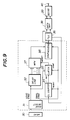
- FIG.9 shows an essential part of the first embodiment.
- the read out apparatus shown in FIG.9 includes an optical head 30, an edge detection circuit 31, a delay line 32, a latch circuit 33, a counter 34, a synthesizing circuit 35, a PLL circuit 36, a multiplexer 37, a data separator 38 and a decoding circuit 39 which are connected as shown.
- a circuit part surrounded by a dotted line corresponds to the edge detection and correction circuit 24 shown in FIG.8.
- the PLL circuit 36, the data separator 38 and the decoding circuit 39 respectively correspond to the PLL circuit 25, the data separator 26 and the decoding circuit 27 shown in FIG.8.
- the illustration of the preamplifier 22 and the waveform equalizer 23 shown in FIG.8 is omitted.
- the head 30 scans the magneto-optic disk 10 (not shown) and supplies a read out signal to the edge detection circuit 31.
- a recording data shown in FIG.10(A) is prerecorded on the magneto-optic disk 10 by turning a recording light beam ON and OFF depending on the recording data as shown in FIG.10(B).
- the read out signal output from the head 30 is shown in FIG.10(C).
- the phase of the rising or falling edges of the read out signal is slightly different from the phase of the ON-pattern of the recording light beam shown in FIG.10(B).
- This difference between the phases is introduced by the change in ambient temperature, inconsistencies among the individual magneto-optic disks 10, the tear drop shape of the magnetic domains formed on the magneto-optic disk 10 and the like. As described above, the leading part and the trailing part of the magnetic domain have different shapes due to the tear drop shape of the magnetic domain.
- the edge detection circuit 31 detects the rising and falling edges of the read out signal, that is, the leading and trailing edges of the recorded magnetic domains.
- the edge detection circuit 31 supplies a leading edge detection signal shown in FIG.10(E) to the delay line 32 and the latch circuit 33, and supplies a trailing edge detection signal shown in FIG.10(D) to the latch circuit 33, the counter 34 and the synthesizing circuit 35.
- the counter 34 is an (n+1)-counter, where n is a natural number.
- the counter 34 receives from the PLL circuit 36 n+1 pulses of a counter clock signal per bit period of the data shown in FIG.10(A).
- the counter 34 is reset in response to a falling edge of the trailing edge detection signal, and thereafter counts up by counting the pulses of the counter clock signal.
- a counted value of the counter 34 is supplied to the latch circuit 33.
- the latch circuit 33 is reset in response to a falling edge of the trailing edge detection signal.
- the latch circuit 33 latches the counted value from the counter 34 in response to a rising edge of the leading edge detection signal, and supplies the latched counted value to the multiplexer 37.
- the delay line 32 receives the leading edge detection signal via a terminal 41 as shown in FIG.11, and delays the leading edge detection signal by an integral multiple of the period of the counter clock signal. As shown in FIG.12, the leading edge detection signal which is output from a terminal d0 of the delay line 32 is delayed by n+1 periods of the counter clock signal, and the leading edge detection signal which is output from a terminal d n is delayed by one period of the counter clock signal. In other words, the leading edge detection signal which is output from a terminal d i of the delay line 32 is delayed by n+1-i periods of the counter clock signal, where i is an integer from 1 to n.
- the delayed leading edge detection signals output from the terminals d0 through d n of the delay line 32 are supplied to corresponding terminals d0 through d n of the multiplexer 37.
- the multiplexer 37 selects the terminal d i which is specified by the counted value i which is obtained from the latch circuit 33 via a terminal 42, and supplies the signal output from the selected terminal d i to the synthesizing circuit 35 via a terminal 43.
- the leading edge detection signal shown in FIG.10(E) is synchronized to the trailing edge detection signal shown in FIG.10(D).
- the synthesizing circuit 35 generates a synthesized signal shown in FIG.10(G) which rises at the rising edge of the signal shown in FIG.10(F) and falls at the falling edge of the signal shown in FIG.10(D). This synthesized signal has the rising edges of the read out signal shown in FIG.10(C) corrected with respect to the falling edges of the read out signal shown in FIG.10(C).
- the synthesized signal output from the synthesizing circuit 35 is supplied to the PLL circuit 36 and to the data separator 38.
- the PLL circuit 36 generates a clock signal which is synchronized to the rising and falling edges of the synthesized signal from the synthesizing circuit 35, and supplies this clock signal to the data separator 38.
- the counter clock signal described above is obtained by frequency-dividing this clock signal in the PLL circuit 36, for example, and is supplied to the counter 34.
- the data separator 38 separates the data from the synthesized signal using the clock signal, and the separated data and the clock signal are supplied to the decoding circuit 39.
- the data output from the data separator 38 takes the form of the run length limited code (RLLC), and the decoding circuit 39 decodes the data into an NRZ code signal.
- the NRZ code signal is output via a terminal 40.
- the leading and trailing edge detection signals which are delayed, phase-shifted and synchronized by the delay line 32 and the multiplexer 37 are synthesized to obtain the synthesized signal.
- the clock signal and the data are extracted from this synthesized signal.
- only one PLL circuit 36 and one data separator 38 are required, and there is no need to provide two independent circuit systems as in the case of the prior art shown in FIG.6. As a result, the scale of the circuit can be greatly reduced compared to the prior art.
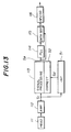
- FIG.13 shows an essential part of the second embodiment, and in FIG.13, those parts which are the same as those corresponding parts in FIG.4 are designated by the same reference numerals, and a description thereof will be omitted.
- an integration circuit 51 and a correction circuit 52 are additionally provided as shown in FIG.13.
- the signal processing circuit 113, the integration circuit 51 and the correction circuit 52 correspond to the edge detection and correction circuit 24 shown in FIG.8.
- the recording light beam is irradiated on the magneto-optic disk at the time of the recording depending on a recording data Dw, so that magnetic domains D of different directions of magnetization are formed in such a manner that the intervals of the edges of the magnetic domains D correspond to the the data "1"s or "0"s of the recording data Dw.
- the intervals of the edges are detected from a read out signal Sr.
- the read out signal Sr which is read out from a VFO pull-in area is integrated so as to obtain a domain length judging signal Sd, and this domain length judging signal Sd is used to judge the expansion and contraction of the recorded magnetic domains D.
- the integration circuit 51 carries out the above integration.
- the correction circuit 52 corrects the edge positions which are obtained from the read out signal Sr using the domain length judging signal Sd, so that it is possible to obtain regular edge positions.
- magnetic domains D having a predetermined length are formed at predetermined intervals on the magneto-optic disk as shown in FIG.14(C) in correspondence with a maximum frequency of a recording data Dw, and a read out signal Sr1 having a duty factor of 50% is obtained as shown in FIG.14(D) when the recorded information is read out from the magneto-optic disk.
- the duty factor of the read out signal does not become 50% as indicated by Sr2 in FIG.15(B) or as indicated by Sr3 in FIG.16(B). If the domain length is equal to the reference value, the integrated value of the read out signal Sr1 becomes zero as shown in FIG.14(E).
- the integrated value of the read out signal Sr2 becomes a positive value as shown in FIG.15(C) if the domain length is longer than the reference value
- the integrated value of the read out signal Sr3 becomes a negative value as shown in FIG.16(C) if the domain length is shorter than the reference value.
- the integrated value of the reference signal Sr (Sr1, Sr2 and Sr3) is used as the domain length judging signal Sd, so as to correct the edge positions of the edge signal Se which is obtained from the data area Md so that the edge positions match the reference positions.
- the recording data Dw which is recorded in the VFO pull-in area according to the 2/7 system is "1001001" as shown in FIG.14(A).
- the recording light beam which is used to record the recording data Dw is turned ON and OFF as shown in FIG.14(B) by a pulse signal having a duty factor of 50%. Accordingly, when the magnetic domains D are formed on the magneto-optic disk in a normal manner, the magnetic domains D having the predetermined length are formed at the predetermined intervals as shown in FIG.14(C).
- the amplifier 112 When the head 111 irradiates the read out light beam on the tracks of the magneto-optic disk which has the magnetic domains D shown in FIG.14(C) formed thereon, the amplifier 112 outputs the read out signal Sr1 shown in FIG.14(D) which has a duty factor of 50%. As in the case of the prior art shown in FIG.4, this read out signal Sr1 is supplied to the signal processing circuit 113 wherein the edge signal Se is formed. But in this embodiment, the read out signal Sr1 is also supplied to the integration circuit 51. This integration circuit 51 outputs the domain length judging signal Sd which indicates the integrated value of the read out signal Sr1, and the domain length judging signal Sd is supplied to the correction circuit 52. Because the duty factor of the read out signal Sr1 is 50% in this case, the integrated value, that is, the domain length judging signal Sd becomes zero as shown in FIG.14(E).
- the duty cycle of the read out signal Sr2 becomes greater than 50% as shown in FIG.15(B).
- the integrated value of the read out signal Sr2 becomes a positive value as shown in FIG.15(C).
- the duty cycle of the read out signal Sr3 becomes less than 50% as shown in FIG.16(B).
- the integrated value of the read out signal Sr3 becomes a negative value as shown in FIG.16(C).
- the integrated value of the read out signal Sr (Sr1, Sr2 and Sr3) obtained from the VFO pull-in area indicates whether or not the length of the domain D is greater than, equal to or less than the reference value.
- the correction circuit 52 can adjust and correct the edge positions which are detected from the read out signal Sr so that the integrated value becomes zero.
- a lowpass filter may be used for the integration circuit 51.
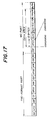
- FIG.17 shows a data format of the information recorded on the magneto-optic disk in conformance with the International Standard Organization (ISO) for 5-inch magneto-optic (MO) disks.
- ISO International Standard Organization
- MO 5-inch magneto-optic
- Sm denotes sector mark
- VFO variable frequency oscillator
- AM denotes address mark
- ID denotes identification bits
- PA denotes postamble
- ODF denotes offset detection flag
- Sync denotes synchronizing bits
- Data denotes data field
- ECC error correction code
- CRC cyclic redundancy check code
- resync denotes a resynchronizing field
- Buffer denotes a buffer field.
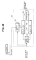
- FIG.18 shows an essential part of the third embodiment, that is, the edge detection and correction circuit 24 shown in FIG.8.
- the edge detection and correction circuit 24 shown in FIG.18 includes an edge detector 61, a voltage variable type delay line 62, a fixed type delay line 63, a synthesizing circuit 64, and a sample integrator 65 which are connected as shown.
- a delay line VCVDL(JPC) on the market may be used as the delay line 62.
- the operating principle of this embodiment is basically the same as that of the second embodiment.
- the delay lines 62 and 63 correspond to the correction circuit 52 shown in FIG.13
- the sample integrator 65 corresponds to the integration circuit 51.
- An analog read out signal shown in FIG.20(A) is obtained from the optical head 10 via the preamplifier 22 and the waveform equalizer 23 shown in FIG.8, and is supplied to the edge detector 61 and the sample integrator 65.
- the edge detector 61 detects the leading and trailing edges of the read out signal as shown in FIG.20(B), and generates a leading edge detection signal shown in FIG.20(C) and a trailing edge detection signal shown in FIG.20(E).
- the leading edge detection signal is supplied to the delay line 62 and is delayed into a delayed leading edge detection signal shown in FIG.20(D).
- the trailing edge detection signal is supplied to the delay line 63 and is delayed into a delayed trailing edge detection signal shown in FIG.20(F).
- the sample integrator 65 integrates the analog read out signal shown in FIG.20(A) when a VFO gate is enabled, that is, when the VFO gate signal has a high level.
- FIG.19 shows an embodiment of the sample integrator 65.
- the sample integrator 65 shown in FIG.19 includes a level shift circuit 651, an analog switch 652, operational amplifiers (or buffers) 653 and 654, a field effect transistor (FET) 655, an integrating capacitor 656, and resistors 657 and 658 which are connected as shown.
- FET field effect transistor
- the analog read out signal is supplied to the buffer 653 via the resistor 658.
- the FET 655 is turned OFF via the level shift circuit 651.
- the analog switch 652 is turned ON and the capacitor 656 discharges so that the charge stored therein is zero.
- the analog switch 652 is turned OFF and the FET 655 is turned ON.
- the analog read out signal supplied to the buffer 653 is transferred to an integrating circuit when the FET 655 turns ON, where this integrating circuit is made up of the capacitor 656 and the operational amplifier 654. Hence, the integrated value is corrected to a corrected value Vc.
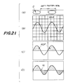
- FIG.21 shows the case where the recorded magnetic domains D and the gaps therebetween are formed with a duty factor of 50%.
- (A) shows the magnetic domains D formed on the recording track of the magneto-optic disk
- (B) shows the waveform of the analog read out signal
- (C) shows a model of the analog read out signal waveform
- (D) shows the integrated value of the read out signal waveform.
- a hatched area RDP corresponds to the magnetic domain D.
- the integrated value that is, the corrected value Vc, becomes the center value (zero or reference level) of the read out signal waveform as shown in (D).
- FIG.22 shows the case where the recorded magnetic domains D are formed with a duty factor greater than 50% with respect to the gaps formed therebetween.
- (A) shows the magnetic domains D formed on the recording track of the magneto-optic disk
- (B) shows the waveform of the analog read out signal
- (C) shows a model of the analog read out signal waveform
- (D) shows the integrated value of the read out signal waveform.
- a hatched area RDP corresponds to the magnetic domain D.
- the integrated value that is, the corrected value Vc, becomes greater than the reference level of the read out signal waveform as shown in (D).
- FIG.23 shows the case where the recorded magnetic domains D are formed with a duty factor less than 50% with respect to the gaps formed therebetween.
- (A) shows the magnetic domains D formed on the recording track of the magneto-optic disk
- (B) shows the waveform of the analog read out signal
- (C) shows a model of the analog read out signal waveform
- (D) shows the integrated value of the read out signal waveform.
- a hatched area RDP corresponds to the magnetic domain D.
- the integrated value that is, the corrected value Vc, becomes smaller than the reference level of the read out signal waveform as shown in (D).
- the corrected value Vc is supplied to the delay line 62 shown in FIG.18.
- the delay line 62 introduces a large delay for a large corrected value Vc and introduces a small delay for a small corrected value Vc.
- the leading edge detection signal shown in FIG.20(C) is delayed by a total delay time TT of t0+t c as shown in FIG.20(D), and the trailing edge detection signal shown in FIG.20(E) is delayed by a time t0 as shown in FIG.20(F).
- both the leading edge detection signal and the trailing edge detection signal are delayed by a time t0.
- the leading edge detection signal is delayed by a total delay time TT of t0-t c ′, where t c ′ ⁇ t0, and the trailing edge detection signal is delayed by a time t0.
- the delayed leading edge detection signal from the delay line 62 and the delayed trailing edge detection signal from the delay line 63 are supplied to the synthesizing circuit 64 and formed into a digital read out signal shown in FIG.20(G).
- the synthesizing circuit 64 may be made up of an OR circuit.
- the above described operation is carried out for the VFO area, and the delay time must be held during read out of the data area. It is possible to use a large capacitance to hold the delay time for a relatively long time. However, if the number of sectors is small and one data area is relatively long, it is difficult to hold the delay time for the relatively long time.
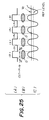
- FIG.24 shows an essential part of the fourth embodiment.
- those parts which are basically the same as those corresponding parts in FIG.18 are designated by the same reference numerals, and a description thereof will be omitted.
- the edge detection and correction circuit 24 shown in FIG.24 includes the edge detector 61, the fixed type delay line 63, the synthesizing circuit 64, a binarization circuit 71, a sample integrator 72, an analog-to-digital (A/D) converter 73, a digital delay line 74 and a multiplexer 75 which are connected as shown.
- the analog read out signal is not integrated directly, but integrated after being digitized.
- the delay line 74 used is not a voltage variable type but a digital type. This delay line 74 provides different delay times digitally, and thus, the A/D converter 73 is used to select the desired delay time by digitizing the integrated (or corrected) value Vc.
- the VFO data is a continuous signal of 1.5 ⁇ intervals.
- the duty factor of the recorded magnetic domains D is greater than 50% as shown in FIG.25(B)
- the analog read out signal becomes as shown in FIG.25(C).
- the solid horizontal line indicates the corrected value Vc and a dotted horizontal line indicates the reference level.
- the delayed leading edge detection signal from the multiplexer 75 and the delayed trailing edge detection signal from the delay line 63 are supplied to the synthesizing circuit 64, and the operation thereafter is the same as that of the third embodiment shown in FIG.18.
- a programmable ECL I/O delay line EPDION(JPC) which is on the market may be used for the digital delay line 74.
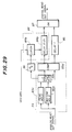
- FIG.28 shows an essential part of this embodiment, and in FIG.28, those parts which are the same as those corresponding parts in FIG.8 are designated by the same reference numerals, and a description thereof will be omitted.
- the read out apparatus shown in FIG.28 includes the optical head 21, the waveform equalizer 23, an edge detector 83, a programmable delay line 84, a delay line 85, an A/D converter 86, an OR circuit 87, a PLL circuit 25, a data separator 26 and a decoding circuit 27 which are connected as shown.
- the read out signal output from the head 21 is supplied to the waveform equalizer 23.
- This waveform equalizer 23 includes an automatic gain control (AGC) circuit, a filter, an equalizer and the like.
- the read out signal is amplified and eliminated to its unwanted components in the waveform equalizer 23.
- the read out signal from the waveform equalizer 23 is supplied to the edge detector 83 which detects the rising and falling edges of the read out signal, that is, the leading and trailing edges of the magnetic domains D recorded on the magneto-optic disk 10 (not shown in FIG.28).
- the edge detector 83 supplies the leading edge detection signal to the programmable delay line 84 and the trailing edge detection signal to the delay line 85.
- the edge detector 83 also generates a slice level signal from the read out signal, and supplies the slice level signal to the A/D converter 86.
- the A/D converter 86 converts the slice level signal into a digital value, and supplies this digital value to the programmable delay line 84.
- the delay time of the programmable delay line 84 is selected from 0 to 2T depending on the digital value received from the A/D converter 86.
- the delay lines 84 and 85 respectively delay the leading edge detection signal and the trailing edge detection signal, and the delayed signals are supplied to the OR circuit 87.
- An output signal of the OR circuit is supplied to the PLL circuit 25 and to the data separator 26. The operation thereafter is the same as that of the block system shown in FIG.8.
- the edge detector 83, the programmable delay line 84, the delay line 85, the A/D converter 86 and the OR circuit 87 correspond to the edge detection and correction circuit 24 shown in FIG.8.
- FIG.29 shows an essential part of the block system shown in FIG.28.
- the edge detector 83 shown in FIG.29 includes a peak hold circuit 83a, a bottom hold circuit 83b, a slice level generating circuit 83c and a comparator 83d which are connected as shown.
- the programmable delay line 84 includes a latch circuit 84a and a variable delay line 84b which are connected as shown.
- the peak hold circuit 83a detects and holds the peak value of the analog read out signal, and supplies the peak value to the slice level generating circuit 83c.
- the bottom hold circuit 83b detects and holds the bottom values of the analog read out signal, and supplies the bottom value to the slice level generating circuit 83c.
- the slice level generating circuit 83c detects an approximate center level between the peak and bottom values, and outputs a slice level signal indicative of this approximate center level (slice level).
- the slice level signal is supplied to the comparator 83d and to the programmable delay line 84 via the A/D converter 86.
- the comparator 83d compares the slice level signal and the analog read out signal, and outputs a pulse signal which has a high level when the analog read out signal is greater than the slice level signal and has a low level when the analog read out signal is smaller than the slice level signal, and outputs a leading edge detection signal and a trailing edge detection signal which are generated from the pulse signal.
- the leading edge detection signal rises in synchronism with the rising edge of the pulse signal, and the trailing edge detection signal falls in synchronism with the falling edge of the pulse signal.
- the leading edge detection signal is supplied to the variable delay line 84b, while the trailing edge detection signal is supplied to the fixed delay line 85.
- the latch circuit 84a receives a digital value which is obtained by digitally converting the slice level signal in the A/D converter 86. This digital value corresponds to the corrected digital value of the fourth embodiment.
- the latch circuit 84a also receives a VFO gate signal, and latches the digital value during a high-level period of the VFO gate signal.
- the digital value is supplied to the variable delay line 84b and determines the delay time of the leading edge detection signal to a time of 0 to 2t.
- FIG.30 shows the relationship between the delay time of the leading edge detection signal and the digital value.
- the delay time of the variable delay line 84b is determined by the slice level SL of the analog read out signal obtained from the VFO pull-in area.
- the trailing edge detection signal is delayed by a fixed time t in the delay line 85.
- FIG.31 generally shows a data format on the magneto-optic disk.
- each track on the magneto-optic disk is divided into ten-odd sectors to several tens of sectors.
- a sector mark SM which indicates the start of the sector is arranged at the head of each sector, and an identification number ID which specifies each sector is arranged following the sector mark SM.
- the sector mark SM and the identification number ID are recorded in the form of physical pits at ⁇ /4, where ⁇ denotes the wavelength.
- Pull-in domains are recorded in the VFO pull-in area, and phase adjusting domains are recorded in the synchronized byte area SB, both by magnetic means.
- the data are recorded in a data area DATA.
- the VFO pull-in domains are made up of magnetic domains having a predetermined length and arranged at predetermined intervals.
- the data format is shown in more detail in FIG.17.
- the VFO gate signal shown in FIG.31 is generated based on a read gate signal ReadGate and a gate signal DTRD.
- the read gate signal ReadGate is used for reading the data shown at an upper part of FIG.31, while the gate signal DTRD is used to read the VFO, SB and DATA.
- the VFO, SB and DATA are read during a time period in which both the gate signals ReadGate and DTRD have the high level.
- FIG.32(A) shows a recording data which is recorded in the VFO pull-in area of the magneto-optic disk when the magnetic domains D have a duty factor of 50% with respect to gaps therebetween.
- the recording data is made up of pulses occurring at 1.5t intervals.
- the slice level SL has the same level as the reference level of the analog read out signal as shown in FIG.32(B).
- the trailing edge detection signal is delayed by the delay time t in the delay line 85, and no correction is made by also delaying the leading edge detection signal by the delay time t in the variable delay line 84b.
- the waveform of the analog read out signal is distorted and the slice level SL shifts in a direction so as to adjust the duty factor of the magnetic domains D to 50%. More particularly, the slice level SL is shifted in a positive direction relative to the reference level.
- the leading edge detection signal is delayed by a delay time of t to 2t in the variable delay line 84b because the slice level SL is greater than the reference level.
- the delay time of the leading edge detection signal becomes longer than the delay time of the trailing edge detection signal, and it is possible to correct the expanded magnetic domains D since the time interval between the leading and trailing edges of the read out signal is shortened.
- the waveform of the analog read out signal is distorted and the slice level SL shifts in a direction so as to adjust the duty factor of the magnetic domains D to 50%. More particularly, the slice level SL is shifted in a negative direction relative to the reference level.
- the leading edge detection signal is delayed by a delay time of 0 to t in the variable delay line 84b because the slice level SL is smaller than the reference level.
- the delay time of the leading edge detection signal becomes shorter than the delay time of the trailing edge detection signal, and it is possible to correct the contracted magnetic domains D since the time interval between the leading and trailing edges of the read out signal is lengthened.
- the detected leading edges of the magnetic domains are corrected so as to prevent undesirable effects of the error caused by the change in ambient temperature, inconsistencies among the individual magneto-optic disks, tear drop shape of the magnetic domains and the like.
- it is unnecessary to provide two circuit systems as in the case of the prior art shown in FIG.6, and the circuit construction becomes simple.
- the VFO pull-in area is provided for each sector of the magneto-optic disk, it is possible to carry out the correction for each sector of the magneto-optic disk.
Landscapes
- Engineering & Computer Science (AREA)
- Signal Processing (AREA)
- Signal Processing For Digital Recording And Reproducing (AREA)
Applications Claiming Priority (6)
| Application Number | Priority Date | Filing Date | Title |
|---|---|---|---|
| JP57328/91 | 1991-03-20 | ||
| JP05732891A JP3556233B2 (ja) | 1991-03-20 | 1991-03-20 | 光磁気ディスクの再生方式 |
| JP136405/91 | 1991-06-07 | ||
| JP3136405A JPH04360048A (ja) | 1991-06-07 | 1991-06-07 | 光磁気ディスクの再生方法及び装置 |
| JP275713/91 | 1991-10-23 | ||
| JP3275713A JP2664302B2 (ja) | 1991-10-23 | 1991-10-23 | 光磁気ディスク再生装置 |
Publications (3)
| Publication Number | Publication Date |
|---|---|
| EP0505253A2 true EP0505253A2 (fr) | 1992-09-23 |
| EP0505253A3 EP0505253A3 (en) | 1993-01-13 |
| EP0505253B1 EP0505253B1 (fr) | 1997-09-24 |
Family
ID=27296215
Family Applications (1)
| Application Number | Title | Priority Date | Filing Date |
|---|---|---|---|
| EP92400687A Expired - Lifetime EP0505253B1 (fr) | 1991-03-20 | 1992-03-16 | Appareil de réproduction d'information à partir d'un disque magnéto-optique |
Country Status (5)
| Country | Link |
|---|---|
| US (1) | US5235590A (fr) |
| EP (1) | EP0505253B1 (fr) |
| KR (1) | KR950010327B1 (fr) |
| CA (1) | CA2063189C (fr) |
| DE (1) | DE69222335T2 (fr) |
Cited By (1)
| Publication number | Priority date | Publication date | Assignee | Title |
|---|---|---|---|---|
| EP0709845A3 (fr) * | 1994-10-31 | 1998-12-30 | Samsung Electronics Co., Ltd. | Appareil d'enregistrement de signal numérique |
Families Citing this family (29)
| Publication number | Priority date | Publication date | Assignee | Title |
|---|---|---|---|---|
| JPH05225638A (ja) * | 1992-02-10 | 1993-09-03 | Sony Corp | 光磁気ディスク再生装置 |
| JP2618571B2 (ja) * | 1992-09-24 | 1997-06-11 | 富士通株式会社 | 光磁気ディスクのデータ再生回路 |
| US5490126A (en) * | 1993-04-07 | 1996-02-06 | Matsushita Electric Industrial Co., Ltd. | Apparatus for recording and reproducing data on a disk |
| JPH06302042A (ja) * | 1993-04-15 | 1994-10-28 | Hitachi Ltd | 光磁気ディスク装置 |
| JPH07182705A (ja) * | 1993-12-21 | 1995-07-21 | Fujitsu Ltd | 光磁気媒体及びその再生装置 |
| US5502711A (en) * | 1995-03-20 | 1996-03-26 | International Business Machines Corporation | Dual digital phase locked loop clock channel for optical recording |
| US5930216A (en) * | 1996-04-19 | 1999-07-27 | Asahi Kasei Microsystems Co., Ltd. | Clock combining circuit |
| US5835542A (en) * | 1996-07-19 | 1998-11-10 | Utek Semiconductor Corporation | Digital data separator for separating data signals from clock signals in an encoded data stream |
| JP2919380B2 (ja) * | 1996-08-29 | 1999-07-12 | 山形日本電気株式会社 | ディスク回転速度制御回路 |
| US5966356A (en) * | 1996-11-11 | 1999-10-12 | Konica Corporation | Optimum slice level signal reading apparatus for optical disk |
| WO2000042609A1 (fr) * | 1999-01-18 | 2000-07-20 | Fujitsu Limited | Procede et dispositif de commande de signal reproduit |
| JP2004538703A (ja) * | 2001-08-03 | 2004-12-24 | コーニンクレッカ フィリップス エレクトロニクス エヌ ヴィ | アナログfirフィルタ |
| US7272201B2 (en) * | 2003-08-20 | 2007-09-18 | Schweitzer Engineering Laboratories, Inc. | System for synchronous sampling and time-of-day clocking using an encoded time signal |
| US7398411B2 (en) * | 2005-05-12 | 2008-07-08 | Schweitzer Engineering Laboratories, Inc. | Self-calibrating time code generator |
| CA2757376A1 (fr) * | 2009-04-03 | 2010-10-07 | Schweitzer Engineering Laboratories, Inc. | Synchronisation de temps insensible aux defaillances |
| US8351433B2 (en) * | 2009-09-18 | 2013-01-08 | Schweitzer Engineering Laboratories Inc | Intelligent electronic device with segregated real-time ethernet |
| US8867345B2 (en) * | 2009-09-18 | 2014-10-21 | Schweitzer Engineering Laboratories, Inc. | Intelligent electronic device with segregated real-time ethernet |
| US8812256B2 (en) | 2011-01-12 | 2014-08-19 | Schweitzer Engineering Laboratories, Inc. | System and apparatus for measuring the accuracy of a backup time source |
| US9324122B2 (en) | 2012-10-19 | 2016-04-26 | Schweitzer Engineering Laboratories, Inc. | Voting scheme for time alignment |
| US9300591B2 (en) | 2013-01-28 | 2016-03-29 | Schweitzer Engineering Laboratories, Inc. | Network device |
| US9620955B2 (en) | 2013-03-15 | 2017-04-11 | Schweitzer Engineering Laboratories, Inc. | Systems and methods for communicating data state change information between devices in an electrical power system |
| US9270109B2 (en) | 2013-03-15 | 2016-02-23 | Schweitzer Engineering Laboratories, Inc. | Exchange of messages between devices in an electrical power system |
| US9065763B2 (en) | 2013-03-15 | 2015-06-23 | Schweitzer Engineering Laboratories, Inc. | Transmission of data over a low-bandwidth communication channel |
| US9967135B2 (en) | 2016-03-29 | 2018-05-08 | Schweitzer Engineering Laboratories, Inc. | Communication link monitoring and failover |
| US10819727B2 (en) | 2018-10-15 | 2020-10-27 | Schweitzer Engineering Laboratories, Inc. | Detecting and deterring network attacks |
| US11522358B2 (en) | 2020-05-18 | 2022-12-06 | Schweitzer Engineering Laboratories, Inc. | Isolation of protective functions in electrical power systems |
| US12105490B2 (en) | 2021-10-04 | 2024-10-01 | Schweitzer Engineering Laboratories, Inc. | Isolation of protection functions in electrical power systems |
| US11862958B2 (en) | 2021-10-04 | 2024-01-02 | Schweitzer Engineering Laboratories, Inc. | Isolation of protection functions in electrical power systems during startup |
| US12498938B2 (en) | 2021-11-10 | 2025-12-16 | Schweitzer Engineering Laboratories, Inc. | Basic input/output system (BIOS) boot check |
Family Cites Families (7)
| Publication number | Priority date | Publication date | Assignee | Title |
|---|---|---|---|---|
| US4646103A (en) * | 1985-03-20 | 1987-02-24 | Hitachi, Ltd. | Optical recording method |
| JP2607462B2 (ja) * | 1985-03-20 | 1997-05-07 | 株式会社日立製作所 | 情報再生方法及び装置 |
| JPH0721897B2 (ja) * | 1986-04-24 | 1995-03-08 | インタ−ナショナル ビジネス マシ−ンズ コ−ポレ−ション | 光磁気データ記録装置 |
| JP2810035B2 (ja) * | 1986-08-22 | 1998-10-15 | 株式会社日立製作所 | 光学的記録再生方法 |
| KR910003460B1 (ko) * | 1987-02-12 | 1991-05-31 | 가부시기가이샤 히다찌세이사꾸쇼 | 광학식 정보기록 장치 |
| US4866691A (en) * | 1987-03-13 | 1989-09-12 | Pioneer Electronic Corporation | AC amplifying RF signal processing circuit for optical disk player |
| JPH073710B2 (ja) * | 1987-06-17 | 1995-01-18 | 日本電気株式会社 | 光磁気ディスク装置 |
-
1992
- 1992-03-13 US US07/851,537 patent/US5235590A/en not_active Expired - Lifetime
- 1992-03-16 DE DE69222335T patent/DE69222335T2/de not_active Expired - Fee Related
- 1992-03-16 EP EP92400687A patent/EP0505253B1/fr not_active Expired - Lifetime
- 1992-03-17 CA CA002063189A patent/CA2063189C/fr not_active Expired - Fee Related
- 1992-03-19 KR KR1019920004515A patent/KR950010327B1/ko not_active Expired - Fee Related
Cited By (1)
| Publication number | Priority date | Publication date | Assignee | Title |
|---|---|---|---|---|
| EP0709845A3 (fr) * | 1994-10-31 | 1998-12-30 | Samsung Electronics Co., Ltd. | Appareil d'enregistrement de signal numérique |
Also Published As
| Publication number | Publication date |
|---|---|
| CA2063189C (fr) | 1996-01-02 |
| KR950010327B1 (ko) | 1995-09-14 |
| EP0505253A3 (en) | 1993-01-13 |
| KR920018680A (ko) | 1992-10-22 |
| EP0505253B1 (fr) | 1997-09-24 |
| US5235590A (en) | 1993-08-10 |
| DE69222335D1 (de) | 1997-10-30 |
| CA2063189A1 (fr) | 1992-09-21 |
| DE69222335T2 (de) | 1998-01-29 |
Similar Documents
| Publication | Publication Date | Title |
|---|---|---|
| EP0505253B1 (fr) | Appareil de réproduction d'information à partir d'un disque magnéto-optique | |
| US4835759A (en) | Method and apparatus for compensating variation of read data in an optical data storage | |
| US4748611A (en) | Information recording medium and method for reproducing the same | |
| US5233589A (en) | Method for recording/reproducing information having a function of correcting variations in the interval in reproduced data and apparatus for realizing same | |
| EP0887790B1 (fr) | Dispositif de reproduction optique et système de mémoire optique comprenant ce dispositif et un support de mémoire optique | |
| US6633443B1 (en) | Peak shift correction circuit and magnetic storage medium playback apparatus | |
| JP3519309B2 (ja) | 光ディスク、光再生装置及び光記録装置 | |
| EP0640967B1 (fr) | Appareil et méthode de détection de marques de synchronisation | |
| EP0407094B1 (fr) | Dispositif de reproduction pour signaux numériques | |
| US5623467A (en) | Data recording apparatus for recording data in sector units | |
| US5359586A (en) | Read out apparatus for reading out information from magneto-optic disk | |
| US5282185A (en) | Apparatus for generating a data signal at an optimal phase | |
| US5623468A (en) | Disk apparatus for detecting address marks from a recording disk having data recorded in a zoned constant angular velocity type system | |
| JP2664302B2 (ja) | 光磁気ディスク再生装置 | |
| JPH0554554A (ja) | 情報記録再生方法及びその装置 | |
| JP2002208144A (ja) | 光ディスク及び光ディスク再生装置 | |
| JP3049155B2 (ja) | 光ディスク再生方法及びその装置 | |
| JP2899477B2 (ja) | 光ディスク装置 | |
| JP2002092874A (ja) | ビットアキュレートな光学ドライブにおける位相不連続性の補償 | |
| EP0311691A1 (fr) | Appareils d'enregistrement/reproduction optique | |
| US7660216B2 (en) | Disk reproducing apparatus and method | |
| JP2852751B2 (ja) | データ再生方法及び装置 | |
| JPH08180588A (ja) | 再生データの抜き出し装置 | |
| JPH1074367A (ja) | クロック・コンバイン回路 | |
| EP1441519A1 (fr) | Dispositif de commande de vitesse de tambour à têtes pour appareil d'enregistrement à cassettes vidéo à définition standard. |
Legal Events
| Date | Code | Title | Description |
|---|---|---|---|
| PUAI | Public reference made under article 153(3) epc to a published international application that has entered the european phase |
Free format text: ORIGINAL CODE: 0009012 |
|
| AK | Designated contracting states |
Kind code of ref document: A2 Designated state(s): DE ES FR GB IT NL SE |
|
| PUAL | Search report despatched |
Free format text: ORIGINAL CODE: 0009013 |
|
| AK | Designated contracting states |
Kind code of ref document: A3 Designated state(s): DE ES FR GB IT NL SE |
|
| 17P | Request for examination filed |
Effective date: 19930208 |
|
| 17Q | First examination report despatched |
Effective date: 19950614 |
|
| GRAG | Despatch of communication of intention to grant |
Free format text: ORIGINAL CODE: EPIDOS AGRA |
|
| GRAH | Despatch of communication of intention to grant a patent |
Free format text: ORIGINAL CODE: EPIDOS IGRA |
|
| GRAH | Despatch of communication of intention to grant a patent |
Free format text: ORIGINAL CODE: EPIDOS IGRA |
|
| GRAA | (expected) grant |
Free format text: ORIGINAL CODE: 0009210 |
|
| AK | Designated contracting states |
Kind code of ref document: B1 Designated state(s): DE ES FR GB IT NL SE |
|
| PG25 | Lapsed in a contracting state [announced via postgrant information from national office to epo] |
Ref country code: IT Free format text: LAPSE BECAUSE OF FAILURE TO SUBMIT A TRANSLATION OF THE DESCRIPTION OR TO PAY THE FEE WITHIN THE PRESCRIBED TIME-LIMIT;WARNING: LAPSES OF ITALIAN PATENTS WITH EFFECTIVE DATE BEFORE 2007 MAY HAVE OCCURRED AT ANY TIME BEFORE 2007. THE CORRECT EFFECTIVE DATE MAY BE DIFFERENT FROM THE ONE RECORDED. Effective date: 19970924 Ref country code: ES Free format text: THE PATENT HAS BEEN ANNULLED BY A DECISION OF A NATIONAL AUTHORITY Effective date: 19970924 |
|
| REF | Corresponds to: |
Ref document number: 69222335 Country of ref document: DE Date of ref document: 19971030 |
|
| PG25 | Lapsed in a contracting state [announced via postgrant information from national office to epo] |
Ref country code: SE Effective date: 19971224 |
|
| ET | Fr: translation filed | ||
| PLBE | No opposition filed within time limit |
Free format text: ORIGINAL CODE: 0009261 |
|
| STAA | Information on the status of an ep patent application or granted ep patent |
Free format text: STATUS: NO OPPOSITION FILED WITHIN TIME LIMIT |
|
| 26N | No opposition filed | ||
| REG | Reference to a national code |
Ref country code: GB Ref legal event code: IF02 |
|
| PGFP | Annual fee paid to national office [announced via postgrant information from national office to epo] |
Ref country code: FR Payment date: 20060308 Year of fee payment: 15 |
|
| PGFP | Annual fee paid to national office [announced via postgrant information from national office to epo] |
Ref country code: NL Payment date: 20060315 Year of fee payment: 15 Ref country code: GB Payment date: 20060315 Year of fee payment: 15 |
|
| GBPC | Gb: european patent ceased through non-payment of renewal fee |
Effective date: 20070316 |
|
| NLV4 | Nl: lapsed or anulled due to non-payment of the annual fee |
Effective date: 20071001 |
|
| REG | Reference to a national code |
Ref country code: FR Ref legal event code: ST Effective date: 20071130 |
|
| PG25 | Lapsed in a contracting state [announced via postgrant information from national office to epo] |
Ref country code: NL Free format text: LAPSE BECAUSE OF NON-PAYMENT OF DUE FEES Effective date: 20071001 |
|
| PG25 | Lapsed in a contracting state [announced via postgrant information from national office to epo] |
Ref country code: GB Free format text: LAPSE BECAUSE OF NON-PAYMENT OF DUE FEES Effective date: 20070316 |
|
| PG25 | Lapsed in a contracting state [announced via postgrant information from national office to epo] |
Ref country code: FR Free format text: LAPSE BECAUSE OF NON-PAYMENT OF DUE FEES Effective date: 20070402 |
|
| PGFP | Annual fee paid to national office [announced via postgrant information from national office to epo] |
Ref country code: DE Payment date: 20090313 Year of fee payment: 18 |
|
| PG25 | Lapsed in a contracting state [announced via postgrant information from national office to epo] |
Ref country code: DE Free format text: LAPSE BECAUSE OF NON-PAYMENT OF DUE FEES Effective date: 20101001 |