EP0501593B1 - Schicht-Typ Widerstand - Google Patents
Schicht-Typ Widerstand Download PDFInfo
- Publication number
- EP0501593B1 EP0501593B1 EP92201179A EP92201179A EP0501593B1 EP 0501593 B1 EP0501593 B1 EP 0501593B1 EP 92201179 A EP92201179 A EP 92201179A EP 92201179 A EP92201179 A EP 92201179A EP 0501593 B1 EP0501593 B1 EP 0501593B1
- Authority
- EP
- European Patent Office
- Prior art keywords
- film
- substrate
- coating
- resistive film
- end caps
- Prior art date
- Legal status (The legal status is an assumption and is not a legal conclusion. Google has not performed a legal analysis and makes no representation as to the accuracy of the status listed.)
- Expired - Lifetime
Links
Images
Classifications
-
- H—ELECTRICITY
- H01—ELECTRIC ELEMENTS
- H01C—RESISTORS
- H01C7/00—Non-adjustable resistors formed as one or more layers or coatings; Non-adjustable resistors made from powdered conducting material or powdered semi-conducting material with or without insulating material
- H01C7/006—Thin film resistors
-
- H—ELECTRICITY
- H01—ELECTRIC ELEMENTS
- H01C—RESISTORS
- H01C1/00—Details
- H01C1/02—Housing; Enclosing; Embedding; Filling the housing or enclosure
- H01C1/034—Housing; Enclosing; Embedding; Filling the housing or enclosure the housing or enclosure being formed as coating or mould without outer sheath
-
- H—ELECTRICITY
- H01—ELECTRIC ELEMENTS
- H01C—RESISTORS
- H01C1/00—Details
- H01C1/14—Terminals or tapping points or electrodes specially adapted for resistors; Arrangements of terminals or tapping points or electrodes on resistors
- H01C1/148—Terminals or tapping points or electrodes specially adapted for resistors; Arrangements of terminals or tapping points or electrodes on resistors the terminals embracing or surrounding the resistive element
-
- H—ELECTRICITY
- H01—ELECTRIC ELEMENTS
- H01C—RESISTORS
- H01C17/00—Apparatus or processes specially adapted for manufacturing resistors
- H01C17/02—Apparatus or processes specially adapted for manufacturing resistors adapted for manufacturing resistors with envelope or housing
-
- H—ELECTRICITY
- H01—ELECTRIC ELEMENTS
- H01C—RESISTORS
- H01C17/00—Apparatus or processes specially adapted for manufacturing resistors
- H01C17/28—Apparatus or processes specially adapted for manufacturing resistors adapted for applying terminals
-
- H—ELECTRICITY
- H01—ELECTRIC ELEMENTS
- H01C—RESISTORS
- H01C7/00—Non-adjustable resistors formed as one or more layers or coatings; Non-adjustable resistors made from powdered conducting material or powdered semi-conducting material with or without insulating material
- H01C7/003—Thick film resistors
-
- Y—GENERAL TAGGING OF NEW TECHNOLOGICAL DEVELOPMENTS; GENERAL TAGGING OF CROSS-SECTIONAL TECHNOLOGIES SPANNING OVER SEVERAL SECTIONS OF THE IPC; TECHNICAL SUBJECTS COVERED BY FORMER USPC CROSS-REFERENCE ART COLLECTIONS [XRACs] AND DIGESTS
- Y10—TECHNICAL SUBJECTS COVERED BY FORMER USPC
- Y10T—TECHNICAL SUBJECTS COVERED BY FORMER US CLASSIFICATION
- Y10T29/00—Metal working
- Y10T29/49—Method of mechanical manufacture
- Y10T29/49002—Electrical device making
- Y10T29/49082—Resistor making
Definitions
- the coating material employed for the above-indicated encapsulation is necessarily at low viscosity. Therefore, as soon as the coating material is applied, by dipping, the resistor is put on a fixture that rotates the resistor about its longitudinal axis. Rotation is continued until the coating material dries. As the result of the rotation, the coating material does not sag, and it is relatively uniform in thickness. Curing of the encapsulating coating is then effected, at high temperature.
- the lead wires that project axially from the end caps are affected so substantially, by the repeated high-temperature cures, that it is conventional to gold plate them.
- the gold plating eliminates or reduces the harm done to the lead wires by the repeated cures.
- gold plating is an expensive step vis-a-vis material especially.
- leads are repeatedly handled during the various process steps indicated above, and which have been employed for years. Typically, therefore, leads become bent. They also become partially covered by environmentally protective material. If follows that final steps in the conventional process for manufacturing the cylindrical resistors include tedious hand dressing, cleaning and straightening operations performed on the lead wires. It is to be understood that, for cosmetic and other reasons important to customers, the leads of the resistors should be straight, clean, and coaxial with the end caps.
- FR-A-1507003 discloses one example of a known resistor including a cylindrical substrate and a film of resistive material provided around the surface of the substrate. A protective layer is formed on the resistive film by immersing the resistor in a metallising solution and then oxidising the resulting metal coating at high temperatures. The ends of the resistor are left unoxidised and metal end caps fitted to the ends.
- US-A-3060063 discloses another prior art process. After the fitting of end caps and lead wires to a cylindrical resistor, the resistor is exposed to chromium halide vapours which form a protective coating. To obtain deposition of the film over all the resistor surface, the resistor is rotated about its longitudinal axis.
- the above descriptive material relates primarily to process difficulties, and attendant increased costs, with regard to conventional cylindrical film-type resistors.
- a film-type resistor comprising:
- Cylindrical film-type resistors thus can have screen-printed environmentally protective coatings, and bare end caps and are highly satisfactory for many applications. This is to be contrasted with cylindrical resistors having dip-applied encapsulating coatings that cover the end caps.
- the present invention goes contrary to encapsulation such as has been conventional for decades.
- encapsulation there is preferably screen printing of an environmentally protective substance onto only the cylindrical substrate and the resistive film thereon, but not including some portions beneath the end caps.
- the end caps are not screen printed.
- the screen-printed coatings do not require rotating in a fixture (or otherwise) for a drying step, since their rheology (viscosity and thixotropy) are such that no rotation is needed. Also, a single-layer screen-printed coating is more environmentally protective than is a single-layer coating applied by dipping.
- the end caps are applied as the last step in the manufacturing operation. Thus, they are not exposed to any firing steps.
- the leads are not bent, nor are they partially (or wholly) covered by environmental protective material. It follows that no gold plating, straightening, cleaning, or dressing is needed.
- the bare end caps are more satisfactory in typical potted electronics packages than are coated end caps.
- a resistive film is first applied to a cylindrical substrate, and is then fired.
- the resistive film is subsequently trimmed to the exact desired resistance value.
- Termination film material is applied to the end portions of the resistive film.
- a screen-printed environmentally protective coating is applied over the resistive film, and is then cured.
- cylindrical end caps having leads extended axially therefrom are press fitted over the ends of the substrate, and are caused to be in effective contact with the termination film material.
- the article has a resistive film, covered by a screen-printed dielectric coating, and further has end caps that are electrically connected to the resistive film.
- the end caps are not covered by the screen-printed dielectric coating.
- the resistive film is screen printed onto the cylindrical substrate, and has a serpentine pattern. There is a gap, extending longitudinally of the substrate, between the corner portions of the serpentine line.
- the environmentally protective coating is screen printed over the serpentine resistive pattern, and also has a longitudinal gap therein. Such latter gap is caused to register with the gap in the serpentine pattern.
- the cylindrical end caps are press fit over the cylindrical substrate sufficiently far that the inner surfaces thereof engage not only the termination film material but also the environmentally protective coating.
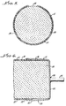
- the thicknesses (and diameters) of the elements shown in Figures 5 and 6 are not to scale.
- the thickness of the resistive film has, in such figures, been exaggerated -- relative to the substrate diameter -- for clarity of illustration.
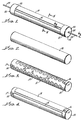
- a typical cylindrical substrate 10 is heat resistant, is preferably formed of a ceramic, and is preferably solid instead of hollow.
- the substrate 10 may have numerous lengths and diameters as desired for particular circuit applications, the sizes ranging from quite large to tiny "toothpick" sizes.
- a resistive film 11 is applied to the exterior cylindrical surface of cylinder 10.
- resistive film 11 is spaced--except for connector portions--from both ends of the substrate.
- film 11 is one created by screen printing since this results in what is known in the art as a "thick film” and, furthermore, since the thickness of the film is uniform and it can be very closely controlled.
- the resistive film may also be what is known in the art as a "thin film", for example, one applied by vapour deposition of a resistive metal.
- resistive film 11 is directly screen printed onto substrate 10 by a suitable screen printing apparatus.
- a suitable screen printing apparatus is described in United States Patent 4,075,968 for Apparatus for Manufacturing Cylindrical Resistors by Thick-Film Silk-Screening.
- the resistive film 11 is in the form of a long strip or line 12 having a serpentine pattern or configuration, with adjacent portions of the serpentine strip being sufficiently close together to effect inductance cancellation.
- adjacent portions of the serpentine strip may be termed "arms".
- the arms are preferably parallel to each other, and each extends circumferentially about the exterior of substrate 10 in a plane perpendicular to the axis of such substrate.
- the above-indicated arms of the serpentine strip connect to each other at bend or base portions 13.
- the bend or base portions are, in the preferred configuration, disposed in two parallel rows extending longitudinally of substrate 10 at opposite sides of a gap 14 in the resistive film 11.
- the gap 14 also extends longitudinally of the substrate.
- the bends 13 are relatively wide, being substantially wider than are the parallel arm portions of strip 12.
- the relatively wide bends 13 minimize the chance that there will be circuit discontinuities when the resistor is trimmed by lapping.
- the substrate 10 with film 11 thereon is fired as described in U.S. patent 3,858,147.
- the screen printed thick-film strip or line 12 has a feathered configuration when viewed in cross-section, reference being made to the left portion of Fig. 6 of the present patent application.
- the longitudinal gap 14 between the parallel rows of bends 13 preferably extends for the full length of substrate 10.
- the width of such gap 14 that is to say the dimension of the gap circumferentially of the substrate, is preferably somewhat greater than the minimum width of gap specified in certain of the above-cited patents. This is to make it more practical to apply to substrate 10 a screen-printed layer of environmentally protective coating having a gap somewhat narrower than gap 14.
- each tail or connector portion 16 of strip 12 there is a tail or connector portion 16 of strip 12, reference being made to the left and right ends of Fig. 3.
- Conductive films 17 may be applied in various ways. They may, for example, be manually applied by means of a brush. They may also be applied by a screen printing operation, or by dipping the ends of the resistor in a pool of the conductive material.
- the films 17 shown in Fig. 3 are quite small, but they may extend over much larger regions, including most or all the way around the substrate as shown and described relative to reference numerals 23 and 24 in patent 3,858,147.
- the resistor is again fired.
- the conductive films 17 minimize contact-resistance problems, providing better connections between the resistive film 11 and the end caps described below.
- the resistive film 11 is then adjusted, vis-a-vis resistance value, so that its resistance is as desired. This is preferably done by lapping as described in U.S. patent 4,132,971 cited above.
- a screen printed environmentally protective coating 19, of dielectric (insulating) substance is applied over the resistive film 11 but not over conductive films 17.
- coating 19 is applied by direct silk screening thereof onto the cylinder 10 over resistive film 11, though not necessarily over those portions of tails 16 that are near films 17.
- Application may be by suitable screen printing apparatus, for example, the one shown and described in patent 4,075,968.
- the screen printed environmental coating 19 preferably covers a portion of the gap 14 between the opposed rows of bends 13. Stated otherwise, the screen printing operation which applies environmental coating 19 is so conducted that there is a longitudinal gap that is registered with gap 14, and that is preferably somewhat narrower than gap 14 in order to ensure that the portions of bends 13 immediately adjacent gap 14 will be covered by the environmental coating 19.
- the above relationship is accomplished by making the permeable area of the screen employed to deposit coating 19 somewhat longer (in the direction of screen movement) than is the permeable area of the screen employed to deposit resistive film 11.
- Coating 19 is preferably rectangular in shape in a developed view (not shown). Stated otherwise, the permeable region of the screen that is used to screen print coating 19 is preferably rectangular in shape.
- the resistor is then heated or fired in order to cure the environmentally protective coating 19.
- the amount of heating, the duration of heating, etc. depend upon the particular coating 19 employed.
- a single-layer coating 19 normally has protective and dielectric properties superior to those of a single layer of silicone conformal (the material conventionally employed for encapsulation of entire cylindrical resistors), it is within the scope of the present invention to provide one or more additional layers of environmentally protective coating 19. After application of each layer, by screen printing, heating or firing is effected to cure the layer as required by the particular substance employed.
- the resistors be rotated about their longitudinal axes prior to or during curing, because the coating substances have such rheologies (viscosities and thixotropies) that the coatings do not sag or flow after screen printing has been performed.
- end caps 20 are press-fit over the ends of cylinder 10, so as to be in physical and electrical contact with conductive films 17.
- the end caps are preferably cylindrical and cup-shaped, as illustrated.
- the end regions of protective coating 19 are sufficiently close to the ends of substrate 10, and the end caps are sufficiently deep, that the rim regions of the end caps telescope over the coating 19 as best illustrated in Figs. 1 and 6.
- each end cap 20 is in effective contact with a conductive layer 17 while, at the same time, rim regions of the end caps are telescoped over and in contact with the screen-printed coating 19.
- the thickness of the coating 19 permits the thickness of the coating 19 to be very accurately controlled.
- the end caps 20 are preferably formed by stamping (more specifically, deep drawing followed by shearing), so that their interior dimensions are also effectively controlled.
- the thicknesses of the coatings 17 and 19, and the dimensions of the interior surfaces of end caps 20, are selected in order to create effective interference fits between the end caps and not only the conductive films 17 but also the dielectric environmentally protective coating 19.
- Each end cap 20 is a highly conductive hollow cylinder 21 preferably formed of a metal, and preferably having a bottom wall 22 that is adjacent the end of substrate 10. Projecting from the bottom wall 22 is a lead 23 that is preferably caused to be coaxial with the end cap 20 and thus with the substrate 10. Each lead 23 is welded to the centre of wall 22 by a weld 24 (Fig. 6). The welding is effected prior to the pressing of the end caps 20 onto the ends of the substrate, and is such that the lead extends perpendicular to the bottom wall 22 as shown.
- the interior surfaces of the end caps 20 at the rim regions thereof are bevelled (divergent in directions away from the ends of the substrate) somewhat. This facilitates pressing of the end caps onto the substrate ends.
- the pressing of the end caps 20 onto the substrate is done carefully, by a suitable pressing tool that permits leads 23 to continue their axially-projecting relationship during all stages of the pressing operation.
- the leads 23 are not bent or adversely affected by the pressing. Since the application of the end caps is the final step in the method, it follows that there is no need to straighten any leads 23, or to remove any material from such leads by cleaning and hand dressing operations. Also, it is not necessary that the leads 23 be gold plated in order to prevent damage thereto during firing operations.
- the environmentally protective coating 19 is formed of a "screen printable" dielectric (insulating) material.
- a "screen printable” dielectric (insulating) material is a resin-type mineral-filled silicone. More specifically, such material is number 240-SB described in bulletin number 42479, by Electro-Science Laboratories, Inc. of Pennsauken, New Jersey.
- Another screen printable material that has been employed by applicant in the present invention is number 242-SB by said Electro-Science Laboratories, Inc.
- Such latter material is a mineral-filled epoxy, and is described in a bulletin promulgated by said Electro-Science Laboratories, Inc. and entitled POLYMER PROTECTIVE COATINGS 242-S, 242-SB, 242-D, the bulletin being numbered 22084.
- a further screen printable substance that has been employed by applicant in the present invention is number 9137, produced by E.I. Du Pont de Nemours & Co. Electronic Materials Division of Wilmington, Delaware. This is described in a Du Pont bulletin entitled "Du Pont Thick Film Dielectric Compositions 5137 and 9137".
- the Du Pont screen printable material is a vitrifying glass frit. It is heated to a peak temperature of about 500°C, this being in contrast with the above-indicated Electro-Science materials that are only heated to temperatures of about 150°C. When a resistor is fired at a high temperature, such as 500°C, its resistance value changes somewhat. Thus, when the Du Pont material is employed, trimming is effected after application of the dielectric screen-printed coating.
- a further screen printable substance that may be employed is a resin-type polyimide. It may be obtained as EPO-TEX 600BLT from Epoxy Technology, Inc. of Billerica, Massachusetts. It also cures at 150°C.
- the substrate 10 is a centerless-ground cylinder of aluminum oxide, having a diameter of 0.250 inch (6.35 mm).
- the resistive film 11 is composed of electrically conductive complex metal oxides in a glass matrix, and has a thickness of 0.0007 inch (17.8 ⁇ m).
- the environmentally protective coating 19 is the above-specified resin-type mineral-filled silicone, and has a thickness of 0.0015 inch (38.1 ⁇ m).
- Each end cap 20 is formed of stainless steel, and has a wall thickness of 0.010 inch (0.25 mm).
- the inner diameter of cylinder 21 is 0.246 inch plus or minus 0.002 inch (50 ⁇ m).
- the conductive coating 17 is a silver-ceramic conductive material in a glass matrix, and has a thickness of 0.001 inch (25 ⁇ m) at regions that contact the exterior cylindrical surface of substrate 10.
- the present article is of high quality, yet may be manufactured by the present method at relatively low cost and with a high rate of production.
Landscapes
- Engineering & Computer Science (AREA)
- Microelectronics & Electronic Packaging (AREA)
- Manufacturing & Machinery (AREA)
- Physics & Mathematics (AREA)
- Electromagnetism (AREA)
- Apparatuses And Processes For Manufacturing Resistors (AREA)
- Non-Adjustable Resistors (AREA)
- Details Of Resistors (AREA)
- Thermistors And Varistors (AREA)
- Semiconductor Lasers (AREA)
Claims (10)
- Schicht-Typ-Widerstand, umfassend:(a) ein zylindrisches Substrat (10);(b) eine Schicht (11) mit Widerstand aufweisendem Material, das um mindestens Teile der äußeren Fläche des Substrates (10) herum vorgesehen ist und an die Oberfläche des Substrates (10) angepaßt ist, wobei die einen Widerstand aufweisende Schicht oder Film (11) einen Spalt (14) besitzt, der sich in Längsrichtung des Substrates erstreckt;(c) einen Überzug (19) aus umgebungsmäßig schützendem Isolationsmaterial, der über der Widerstand aufweisenden Schicht (11) vorgesehen ist, um sie zu isolieren und der Umwelt gegenüber zu schützen; und(d) elektrisch leitende Endkappen (20), die an gegenüberliegenden Enden des Substrates vorgesehen und elektrisch mit den Verbindungsabschnitten (16) verbunden sind, die an den Enden der Widerstand aufweisenden Schicht (11) ausgebildet sind; wobei sich der Überzug (19) nicht über die Endkappen (20) erstreckt, dadurch gekennzeichnet, daß der gegenüber der Umwelt schützende Überzug (19) einen Siebdruck-Überzug darstellt, der eine genau gesteuerte einheitliche Dicke und ebenfalls einen Spalt besitzt, der sich in Längsrichtung des Substrates erstreckt, wobei die Spalte im wesentlichen zueinander mit allen Bereichen der Widerstand aufweisenden Schicht (11) zusammenpassen, anders als die Verbindungsabschnitte (16), die durch den Überzug (19) abgedeckt sind.
- Widerstand nach Anspruch 1, der ferner folgendes umfaßt:
(e) eine hochleitende Abschlußschicht (17), die an den Enden des Substrats aufgetragen wird, um elektrisch die Verbindungsabschnitte (16) der Widerstand aufweisenden Schicht (11) und den Endkappen (20) zu verbinden. - Widerstand nach Anspruch 1 oder 2, bei dem die Endkappen (20) durch Druck auf die Enden des Substrats aufgesetzt sind und mit dem Überzug (19) und mit der Widerstand aufweisenden Schicht (11) oder der leitenden Schicht (17), wenn diese vorgesehen ist, einen Fest- oder Paßsitz bilden.
- Widerstand nach irgendeinem der vorstehenden Ansprüche, bei dem die Widerstandsschicht (11) in einem serpentinenartigen Muster auf das Substrat (10) aufgetragen wird.
- Widerstand nach irgendeinem der vorstehenden Ansprüche, bei denen die Widerstand aufweisende Schicht (11) ein dicker Film ist, der direkt auf das Substrat (10) aufgetragen wird.
- Widerstand nach Anspruch 5, bei dem die Dicke der einen Widerstand aufweisenden Schicht (11) einen Siebdruckfilm darstellt.
- Widerstand nach irgendeinem der vorstehenden Ansprüche, bei dem der umweltmäßig schützende Überzug (19) ein harzartiges mineralgefülltes Silikon oder ein mineralgefülltes Epoxidharz ist.
- Widerstand nach irgendeinem der Ansprüche 1 bis 6, bei dem der Schutzüberzug (19) eine glasartig gewordene Glasfritte oder -masse darstellt.
- Widerstand nach irgendeinem der Ansprüche 1 bis 6, bei dem der Schutzüberzug (19) ein harzartiges Polyimid ist.
- Widerstand nach irgendeinem der vorstehenden Ansprüche, bei dem sich die Endkappen (20) über mindestens einen Teil des Schutzüberzuges (19) erstrecken.
Applications Claiming Priority (3)
| Application Number | Priority Date | Filing Date | Title |
|---|---|---|---|
| US173723 | 1988-03-25 | ||
| US07/173,723 US4866411A (en) | 1988-03-25 | 1988-03-25 | Film-type cylindrical resistor, and method of making it |
| EP89301148A EP0334473B1 (de) | 1988-03-25 | 1989-02-07 | Herstellungsverfahren für einen Dünnschichttyp-Widerstand |
Related Parent Applications (1)
| Application Number | Title | Priority Date | Filing Date |
|---|---|---|---|
| EP89301148.6 Division | 1989-02-07 |
Publications (3)
| Publication Number | Publication Date |
|---|---|
| EP0501593A2 EP0501593A2 (de) | 1992-09-02 |
| EP0501593A3 EP0501593A3 (en) | 1992-11-25 |
| EP0501593B1 true EP0501593B1 (de) | 1995-09-27 |
Family
ID=22633218
Family Applications (2)
| Application Number | Title | Priority Date | Filing Date |
|---|---|---|---|
| EP92201179A Expired - Lifetime EP0501593B1 (de) | 1988-03-25 | 1989-02-07 | Schicht-Typ Widerstand |
| EP89301148A Expired - Lifetime EP0334473B1 (de) | 1988-03-25 | 1989-02-07 | Herstellungsverfahren für einen Dünnschichttyp-Widerstand |
Family Applications After (1)
| Application Number | Title | Priority Date | Filing Date |
|---|---|---|---|
| EP89301148A Expired - Lifetime EP0334473B1 (de) | 1988-03-25 | 1989-02-07 | Herstellungsverfahren für einen Dünnschichttyp-Widerstand |
Country Status (6)
| Country | Link |
|---|---|
| US (1) | US4866411A (de) |
| EP (2) | EP0501593B1 (de) |
| JP (1) | JP2638193B2 (de) |
| AT (2) | ATE85454T1 (de) |
| DE (2) | DE68924431T2 (de) |
| ES (2) | ES2037948T3 (de) |
Families Citing this family (19)
| Publication number | Priority date | Publication date | Assignee | Title |
|---|---|---|---|---|
| US5210516A (en) * | 1990-02-22 | 1993-05-11 | Murata Manufacturing Co., Ltd. | Ptc thermistor and ptc thermistor producing method, and resistor with a ptc thermistor |
| ATE154990T1 (de) * | 1991-04-10 | 1997-07-15 | Caddock Electronics Inc | Schichtwiderstand |
| GB9112726D0 (en) * | 1991-06-13 | 1991-07-31 | Cooper Uk | Electrical fuses |
| EP0532223A1 (de) * | 1991-09-12 | 1993-03-17 | Caddock Electronics, Inc. | Elektrischer Schichtresistant |
| US5304977A (en) * | 1991-09-12 | 1994-04-19 | Caddock Electronics, Inc. | Film-type power resistor combination with anchored exposed substrate/heatsink |
| US5252944A (en) * | 1991-09-12 | 1993-10-12 | Caddock Electronics, Inc. | Film-type electrical resistor combination |
| US5231372A (en) * | 1991-10-09 | 1993-07-27 | Caddock Electronics, Inc. | Method of manufacturing high-voltage and/or high-power thick-film screen-printed cylindrical resistors having small sizes, low voltage coefficients, and low inductance, and resistor thus manufactured |
| US5481241A (en) * | 1993-11-12 | 1996-01-02 | Caddock Electronics, Inc. | Film-type heat sink-mounted power resistor combination having only a thin encapsulant, and having an enlarged internal heat sink |
| DE19744224C2 (de) * | 1997-09-15 | 1999-12-23 | Heraeus Electro Nite Int | Sensor zur Messung von Gaskonzentrationen |
| EP0987545A1 (de) | 1997-09-15 | 2000-03-22 | Heraeus Electro-Nite International N.V. | Röhrchenförmiger Gassensor mit aufgedruckten Sensor- und Heizflächen |
| KR100773413B1 (ko) * | 2000-05-26 | 2007-11-05 | 이동우 | 원통형 저항기의 제조방법 |
| DE102006036100B3 (de) * | 2006-08-02 | 2008-01-24 | Zitzmann, Heinrich, Dr. | Verfahren zur Herstellung eines Temperaturmessfühlers |
| US8089337B2 (en) * | 2007-07-18 | 2012-01-03 | Watlow Electric Manufacturing Company | Thick film layered resistive device employing a dielectric tape |
| US8557082B2 (en) * | 2007-07-18 | 2013-10-15 | Watlow Electric Manufacturing Company | Reduced cycle time manufacturing processes for thick film resistive devices |
| US8061402B2 (en) * | 2008-04-07 | 2011-11-22 | Watlow Electric Manufacturing Company | Method and apparatus for positioning layers within a layered heater system |
| WO2012058414A2 (en) * | 2010-10-27 | 2012-05-03 | Schlumberger Canada Limited | Thick-film resistorized ceramic insulators for sealed high voltage tube electrodes |
| US20140366624A1 (en) * | 2011-12-22 | 2014-12-18 | Endress + Hauser Flowtec Ag | Spacer for a Thermal, Flow Measuring Device |
| TWM450811U (zh) * | 2012-12-13 | 2013-04-11 | Viking Tech Corp | 電阻元件 |
| EP4557320A1 (de) * | 2023-11-15 | 2025-05-21 | Abb Schweiz Ag | Widerstandsstruktur und spannungsteileranordnung |
Family Cites Families (17)
| Publication number | Priority date | Publication date | Assignee | Title |
|---|---|---|---|---|
| FR902076A (fr) * | 1943-02-22 | 1945-08-17 | Philips Nv | Procédé de fabrication de résistances électriques enroulées et résistances fabriquées suivant ce procédé |
| US3060063A (en) * | 1960-06-17 | 1962-10-23 | Int Resistance Co | Electrical resistor and method of making the same |
| FR1507003A (fr) * | 1966-01-11 | 1967-12-22 | Fr De L Electro Resistance Soc | Procédé pour protéger les résistances à couche et résistances protégées par ce procédé |
| GB1314388A (en) * | 1970-07-13 | 1973-04-18 | Fasterr Transformers Ltd | Resistors |
| US3858147A (en) * | 1972-12-14 | 1974-12-31 | R Caddock | Non-inductive film-type cylindrical resistor |
| US3880609A (en) * | 1972-12-14 | 1975-04-29 | Richard E Caddock | Method and apparatus for manufacturing cylindrical resistors by thick-film silk-screening |
| CA968429A (en) * | 1972-12-14 | 1975-05-27 | Richard E. Caddock | Noninductive film-type cylindrical resistor, and method of making the same |
| US3881162A (en) * | 1974-04-01 | 1975-04-29 | Richard E Caddock | Film-type cylindrical resistor and method of manufacturing |
| US3921119A (en) * | 1974-04-01 | 1975-11-18 | Richard E Caddock | Film-type cylindrical resistor |
| US4075968A (en) * | 1974-12-09 | 1978-02-28 | Caddock Richard E | Apparatus for manufacturing cylindrical resistors by thick-film silk-screening |
| JPS5275763U (de) * | 1975-12-05 | 1977-06-06 | ||
| US4132971A (en) * | 1977-02-28 | 1979-01-02 | Caddock Jr Richard E | Noninductive film-type cylindrical resistor and method of making it |
| JPS59231430A (ja) * | 1983-06-14 | 1984-12-26 | Tokyo Electric Co Ltd | ロ−ドセル等のパタ−ン形成部品 |
| FR2566386A1 (fr) * | 1984-06-22 | 1985-12-27 | Labo Electronique Physique | Melange de depart pour une composition isolante comprenant un verre au plomb, encre serigraphiable comportant un tel melange et utilisation de cette encre pour la protection de microcircuits hybrides sur substrat ceramique |
| JPS6165405A (ja) * | 1984-09-07 | 1986-04-04 | 株式会社東芝 | 膜抵抗体の保護膜製造方法 |
| JPS62128514A (ja) * | 1985-11-29 | 1987-06-10 | 株式会社村田製作所 | 磁器電子部品 |
| US4697335A (en) * | 1986-03-31 | 1987-10-06 | Hy-Meg Corporation | Method of manufacturing a film-type electronic device |
-
1988
- 1988-03-25 US US07/173,723 patent/US4866411A/en not_active Expired - Lifetime
-
1989
- 1989-02-07 AT AT89301148T patent/ATE85454T1/de not_active IP Right Cessation
- 1989-02-07 EP EP92201179A patent/EP0501593B1/de not_active Expired - Lifetime
- 1989-02-07 EP EP89301148A patent/EP0334473B1/de not_active Expired - Lifetime
- 1989-02-07 DE DE68924431T patent/DE68924431T2/de not_active Expired - Fee Related
- 1989-02-07 ES ES198989301148T patent/ES2037948T3/es not_active Expired - Lifetime
- 1989-02-07 ES ES92201179T patent/ES2079137T3/es not_active Expired - Lifetime
- 1989-02-07 DE DE8989301148T patent/DE68904667T2/de not_active Expired - Fee Related
- 1989-02-07 AT AT92201179T patent/ATE128573T1/de not_active IP Right Cessation
- 1989-03-24 JP JP1073702A patent/JP2638193B2/ja not_active Expired - Fee Related
Also Published As
| Publication number | Publication date |
|---|---|
| ATE85454T1 (de) | 1993-02-15 |
| EP0501593A2 (de) | 1992-09-02 |
| EP0501593A3 (en) | 1992-11-25 |
| JPH01283801A (ja) | 1989-11-15 |
| ES2037948T3 (es) | 1993-07-01 |
| DE68924431D1 (de) | 1995-11-02 |
| JP2638193B2 (ja) | 1997-08-06 |
| DE68904667D1 (de) | 1993-03-18 |
| EP0334473A2 (de) | 1989-09-27 |
| ATE128573T1 (de) | 1995-10-15 |
| EP0334473B1 (de) | 1993-02-03 |
| DE68924431T2 (de) | 1996-03-07 |
| DE68904667T2 (de) | 1993-06-03 |
| US4866411A (en) | 1989-09-12 |
| ES2079137T3 (es) | 1996-01-01 |
| EP0334473A3 (en) | 1990-09-05 |
Similar Documents
| Publication | Publication Date | Title |
|---|---|---|
| EP0501593B1 (de) | Schicht-Typ Widerstand | |
| JP2726130B2 (ja) | 金属有機物膜からなる少量アンペア用ヒューズ及びその製造方法 | |
| KR102029225B1 (ko) | 궐련형 전자담배 가열기기용 세라믹히터 및 이의 제조방법 | |
| EP0468429B1 (de) | SiC-Dünnschichtthermistor und Verfahren und Herstellungsverfahren. | |
| US4297670A (en) | Metal foil resistor | |
| US4306217A (en) | Flat electrical components | |
| US5257003A (en) | Thermistor and its method of manufacture | |
| US4168520A (en) | Monolithic ceramic capacitor with free-flowed protective coating and method for making same | |
| CA1075829A (en) | Thick film varistor and method of making the same | |
| US3881162A (en) | Film-type cylindrical resistor and method of manufacturing | |
| KR100470797B1 (ko) | 표면 실장형 저항기와 그 제조 방법 | |
| US4138656A (en) | Attachment of leads to electrical components | |
| US4419652A (en) | Temperature sensor | |
| JPH02110903A (ja) | 抵抗体の製造方法 | |
| JPS59501566A (ja) | 電子要素製造方法 | |
| KR0173541B1 (ko) | 곡면 발열형 세라믹 히타와 그의 제조 방법 | |
| JP2718178B2 (ja) | 角板型薄膜チップ抵抗器の製造方法 | |
| JPH10172806A (ja) | 温度センサ及びその製造方法 | |
| JP2718232B2 (ja) | 角板型薄膜チップ抵抗器の製造方法 | |
| JP2866808B2 (ja) | チップ抵抗器の製造方法 | |
| JP2024058882A (ja) | 温度検出器を製造する方法 | |
| JP2718196B2 (ja) | 角板型薄膜チップ抵抗器の製造方法 | |
| JP2000003801A (ja) | 表面実装型抵抗器とその製造方法 | |
| JPH08321402A (ja) | チップ状電子部品およびその製造方法 | |
| JPH0410501A (ja) | 回路素子及びその製造方法 |
Legal Events
| Date | Code | Title | Description |
|---|---|---|---|
| PUAI | Public reference made under article 153(3) epc to a published international application that has entered the european phase |
Free format text: ORIGINAL CODE: 0009012 |
|
| 17P | Request for examination filed |
Effective date: 19920514 |
|
| AC | Divisional application: reference to earlier application |
Ref document number: 334473 Country of ref document: EP |
|
| AK | Designated contracting states |
Kind code of ref document: A2 Designated state(s): AT BE CH DE ES FR GB GR IT LI LU NL SE |
|
| PUAL | Search report despatched |
Free format text: ORIGINAL CODE: 0009013 |
|
| AK | Designated contracting states |
Kind code of ref document: A3 Designated state(s): AT BE CH DE ES FR GB GR IT LI LU NL SE |
|
| 17Q | First examination report despatched |
Effective date: 19940624 |
|
| GRAA | (expected) grant |
Free format text: ORIGINAL CODE: 0009210 |
|
| AC | Divisional application: reference to earlier application |
Ref document number: 334473 Country of ref document: EP |
|
| AK | Designated contracting states |
Kind code of ref document: B1 Designated state(s): AT BE CH DE ES FR GB GR IT LI LU NL SE |
|
| PG25 | Lapsed in a contracting state [announced via postgrant information from national office to epo] |
Ref country code: GR Free format text: LAPSE BECAUSE OF FAILURE TO SUBMIT A TRANSLATION OF THE DESCRIPTION OR TO PAY THE FEE WITHIN THE PRESCRIBED TIME-LIMIT Effective date: 19950927 |
|
| REF | Corresponds to: |
Ref document number: 128573 Country of ref document: AT Date of ref document: 19951015 Kind code of ref document: T |
|
| REF | Corresponds to: |
Ref document number: 68924431 Country of ref document: DE Date of ref document: 19951102 |
|
| ITF | It: translation for a ep patent filed | ||
| PGFP | Annual fee paid to national office [announced via postgrant information from national office to epo] |
Ref country code: LU Payment date: 19960101 Year of fee payment: 8 |
|
| REG | Reference to a national code |
Ref country code: ES Ref legal event code: FG2A Ref document number: 2079137 Country of ref document: ES Kind code of ref document: T3 |
|
| ET | Fr: translation filed | ||
| PGFP | Annual fee paid to national office [announced via postgrant information from national office to epo] |
Ref country code: ES Payment date: 19960215 Year of fee payment: 8 |
|
| PLBE | No opposition filed within time limit |
Free format text: ORIGINAL CODE: 0009261 |
|
| STAA | Information on the status of an ep patent application or granted ep patent |
Free format text: STATUS: NO OPPOSITION FILED WITHIN TIME LIMIT |
|
| 26N | No opposition filed | ||
| PG25 | Lapsed in a contracting state [announced via postgrant information from national office to epo] |
Ref country code: LU Free format text: LAPSE BECAUSE OF NON-PAYMENT OF DUE FEES Effective date: 19970207 |
|
| PG25 | Lapsed in a contracting state [announced via postgrant information from national office to epo] |
Ref country code: ES Free format text: LAPSE BECAUSE OF NON-PAYMENT OF DUE FEES Effective date: 19970208 |
|
| REG | Reference to a national code |
Ref country code: ES Ref legal event code: FD2A Effective date: 19990503 |
|
| GBPC | Gb: european patent ceased through non-payment of renewal fee |
Effective date: 20000207 |
|
| REG | Reference to a national code |
Ref country code: GB Ref legal event code: 728V |
|
| REG | Reference to a national code |
Ref country code: GB Ref legal event code: 728Y Ref country code: GB Ref legal event code: 732E |
|
| REG | Reference to a national code |
Ref country code: GB Ref legal event code: IF02 |
|
| PGFP | Annual fee paid to national office [announced via postgrant information from national office to epo] |
Ref country code: SE Payment date: 20030205 Year of fee payment: 15 |
|
| PGFP | Annual fee paid to national office [announced via postgrant information from national office to epo] |
Ref country code: FR Payment date: 20030210 Year of fee payment: 15 |
|
| PGFP | Annual fee paid to national office [announced via postgrant information from national office to epo] |
Ref country code: AT Payment date: 20030212 Year of fee payment: 15 |
|
| PGFP | Annual fee paid to national office [announced via postgrant information from national office to epo] |
Ref country code: CH Payment date: 20030214 Year of fee payment: 15 |
|
| PGFP | Annual fee paid to national office [announced via postgrant information from national office to epo] |
Ref country code: BE Payment date: 20030425 Year of fee payment: 15 |
|
| PG25 | Lapsed in a contracting state [announced via postgrant information from national office to epo] |
Ref country code: AT Free format text: LAPSE BECAUSE OF NON-PAYMENT OF DUE FEES Effective date: 20040207 |
|
| PG25 | Lapsed in a contracting state [announced via postgrant information from national office to epo] |
Ref country code: SE Free format text: LAPSE BECAUSE OF NON-PAYMENT OF DUE FEES Effective date: 20040208 |
|
| PG25 | Lapsed in a contracting state [announced via postgrant information from national office to epo] |
Ref country code: BE Free format text: LAPSE BECAUSE OF NON-PAYMENT OF DUE FEES Effective date: 20040228 |
|
| PG25 | Lapsed in a contracting state [announced via postgrant information from national office to epo] |
Ref country code: LI Free format text: LAPSE BECAUSE OF NON-PAYMENT OF DUE FEES Effective date: 20040229 Ref country code: CH Free format text: LAPSE BECAUSE OF NON-PAYMENT OF DUE FEES Effective date: 20040229 |
|
| BERE | Be: lapsed |
Owner name: *CADDOCK RICHARD E. Effective date: 20040228 |
|
| EUG | Se: european patent has lapsed | ||
| REG | Reference to a national code |
Ref country code: CH Ref legal event code: PL |
|
| PG25 | Lapsed in a contracting state [announced via postgrant information from national office to epo] |
Ref country code: FR Free format text: LAPSE BECAUSE OF NON-PAYMENT OF DUE FEES Effective date: 20041029 |
|
| REG | Reference to a national code |
Ref country code: FR Ref legal event code: ST |
|
| PG25 | Lapsed in a contracting state [announced via postgrant information from national office to epo] |
Ref country code: IT Free format text: LAPSE BECAUSE OF NON-PAYMENT OF DUE FEES Effective date: 20050207 |
|
| PGFP | Annual fee paid to national office [announced via postgrant information from national office to epo] |
Ref country code: GB Payment date: 20060201 Year of fee payment: 18 |
|
| PGFP | Annual fee paid to national office [announced via postgrant information from national office to epo] |
Ref country code: DE Payment date: 20060202 Year of fee payment: 18 |
|
| PGFP | Annual fee paid to national office [announced via postgrant information from national office to epo] |
Ref country code: NL Payment date: 20060205 Year of fee payment: 18 |
|
| GBPC | Gb: european patent ceased through non-payment of renewal fee |
Effective date: 20070207 |
|
| NLV4 | Nl: lapsed or anulled due to non-payment of the annual fee |
Effective date: 20070901 |
|
| PG25 | Lapsed in a contracting state [announced via postgrant information from national office to epo] |
Ref country code: NL Free format text: LAPSE BECAUSE OF NON-PAYMENT OF DUE FEES Effective date: 20070901 Ref country code: DE Free format text: LAPSE BECAUSE OF NON-PAYMENT OF DUE FEES Effective date: 20070901 |
|
| PG25 | Lapsed in a contracting state [announced via postgrant information from national office to epo] |
Ref country code: GB Free format text: LAPSE BECAUSE OF NON-PAYMENT OF DUE FEES Effective date: 20070207 |