EP0494626A2 - Ferroelektrisches Flüssigkristallelement - Google Patents
Ferroelektrisches Flüssigkristallelement Download PDFInfo
- Publication number
- EP0494626A2 EP0494626A2 EP92100126A EP92100126A EP0494626A2 EP 0494626 A2 EP0494626 A2 EP 0494626A2 EP 92100126 A EP92100126 A EP 92100126A EP 92100126 A EP92100126 A EP 92100126A EP 0494626 A2 EP0494626 A2 EP 0494626A2
- Authority
- EP
- European Patent Office
- Prior art keywords
- liquid crystal
- electric field
- flow
- state
- surface stabilization
- Prior art date
- Legal status (The legal status is an assumption and is not a legal conclusion. Google has not performed a legal analysis and makes no representation as to the accuracy of the status listed.)
- Granted
Links
Images


Classifications
-
- G—PHYSICS
- G09—EDUCATION; CRYPTOGRAPHY; DISPLAY; ADVERTISING; SEALS
- G09G—ARRANGEMENTS OR CIRCUITS FOR CONTROL OF INDICATING DEVICES USING STATIC MEANS TO PRESENT VARIABLE INFORMATION
- G09G3/00—Control arrangements or circuits, of interest only in connection with visual indicators other than cathode-ray tubes
- G09G3/20—Control arrangements or circuits, of interest only in connection with visual indicators other than cathode-ray tubes for presentation of an assembly of a number of characters, e.g. a page, by composing the assembly by combination of individual elements arranged in a matrix no fixed position being assigned to or needed to be assigned to the individual characters or partial characters
- G09G3/34—Control arrangements or circuits, of interest only in connection with visual indicators other than cathode-ray tubes for presentation of an assembly of a number of characters, e.g. a page, by composing the assembly by combination of individual elements arranged in a matrix no fixed position being assigned to or needed to be assigned to the individual characters or partial characters by control of light from an independent source
- G09G3/36—Control arrangements or circuits, of interest only in connection with visual indicators other than cathode-ray tubes for presentation of an assembly of a number of characters, e.g. a page, by composing the assembly by combination of individual elements arranged in a matrix no fixed position being assigned to or needed to be assigned to the individual characters or partial characters by control of light from an independent source using liquid crystals
- G09G3/3611—Control of matrices with row and column drivers
- G09G3/3622—Control of matrices with row and column drivers using a passive matrix
- G09G3/3629—Control of matrices with row and column drivers using a passive matrix using liquid crystals having memory effects, e.g. ferroelectric liquid crystals
-
- G—PHYSICS
- G02—OPTICS
- G02F—OPTICAL DEVICES OR ARRANGEMENTS FOR THE CONTROL OF LIGHT BY MODIFICATION OF THE OPTICAL PROPERTIES OF THE MEDIA OF THE ELEMENTS INVOLVED THEREIN; NON-LINEAR OPTICS; FREQUENCY-CHANGING OF LIGHT; OPTICAL LOGIC ELEMENTS; OPTICAL ANALOGUE/DIGITAL CONVERTERS
- G02F1/00—Devices or arrangements for the control of the intensity, colour, phase, polarisation or direction of light arriving from an independent light source, e.g. switching, gating or modulating; Non-linear optics
- G02F1/01—Devices or arrangements for the control of the intensity, colour, phase, polarisation or direction of light arriving from an independent light source, e.g. switching, gating or modulating; Non-linear optics for the control of the intensity, phase, polarisation or colour
- G02F1/13—Devices or arrangements for the control of the intensity, colour, phase, polarisation or direction of light arriving from an independent light source, e.g. switching, gating or modulating; Non-linear optics for the control of the intensity, phase, polarisation or colour based on liquid crystals, e.g. single liquid crystal display cells
- G02F1/137—Devices or arrangements for the control of the intensity, colour, phase, polarisation or direction of light arriving from an independent light source, e.g. switching, gating or modulating; Non-linear optics for the control of the intensity, phase, polarisation or colour based on liquid crystals, e.g. single liquid crystal display cells characterised by the electro-optical or magneto-optical effect, e.g. field-induced phase transition, orientation effect, guest-host interaction or dynamic scattering
- G02F1/139—Devices or arrangements for the control of the intensity, colour, phase, polarisation or direction of light arriving from an independent light source, e.g. switching, gating or modulating; Non-linear optics for the control of the intensity, phase, polarisation or colour based on liquid crystals, e.g. single liquid crystal display cells characterised by the electro-optical or magneto-optical effect, e.g. field-induced phase transition, orientation effect, guest-host interaction or dynamic scattering based on orientation effects in which the liquid crystal remains transparent
- G02F1/141—Devices or arrangements for the control of the intensity, colour, phase, polarisation or direction of light arriving from an independent light source, e.g. switching, gating or modulating; Non-linear optics for the control of the intensity, phase, polarisation or colour based on liquid crystals, e.g. single liquid crystal display cells characterised by the electro-optical or magneto-optical effect, e.g. field-induced phase transition, orientation effect, guest-host interaction or dynamic scattering based on orientation effects in which the liquid crystal remains transparent using ferroelectric liquid crystals
-
- G—PHYSICS
- G02—OPTICS
- G02F—OPTICAL DEVICES OR ARRANGEMENTS FOR THE CONTROL OF LIGHT BY MODIFICATION OF THE OPTICAL PROPERTIES OF THE MEDIA OF THE ELEMENTS INVOLVED THEREIN; NON-LINEAR OPTICS; FREQUENCY-CHANGING OF LIGHT; OPTICAL LOGIC ELEMENTS; OPTICAL ANALOGUE/DIGITAL CONVERTERS
- G02F1/00—Devices or arrangements for the control of the intensity, colour, phase, polarisation or direction of light arriving from an independent light source, e.g. switching, gating or modulating; Non-linear optics
- G02F1/01—Devices or arrangements for the control of the intensity, colour, phase, polarisation or direction of light arriving from an independent light source, e.g. switching, gating or modulating; Non-linear optics for the control of the intensity, phase, polarisation or colour
- G02F1/13—Devices or arrangements for the control of the intensity, colour, phase, polarisation or direction of light arriving from an independent light source, e.g. switching, gating or modulating; Non-linear optics for the control of the intensity, phase, polarisation or colour based on liquid crystals, e.g. single liquid crystal display cells
- G02F1/137—Devices or arrangements for the control of the intensity, colour, phase, polarisation or direction of light arriving from an independent light source, e.g. switching, gating or modulating; Non-linear optics for the control of the intensity, phase, polarisation or colour based on liquid crystals, e.g. single liquid crystal display cells characterised by the electro-optical or magneto-optical effect, e.g. field-induced phase transition, orientation effect, guest-host interaction or dynamic scattering
- G02F1/13787—Hybrid-alignment cells
-
- G—PHYSICS
- G09—EDUCATION; CRYPTOGRAPHY; DISPLAY; ADVERTISING; SEALS
- G09G—ARRANGEMENTS OR CIRCUITS FOR CONTROL OF INDICATING DEVICES USING STATIC MEANS TO PRESENT VARIABLE INFORMATION
- G09G2310/00—Command of the display device
- G09G2310/02—Addressing, scanning or driving the display screen or processing steps related thereto
- G09G2310/0202—Addressing of scan or signal lines
- G09G2310/0205—Simultaneous scanning of several lines in flat panels
-
- G—PHYSICS
- G09—EDUCATION; CRYPTOGRAPHY; DISPLAY; ADVERTISING; SEALS
- G09G—ARRANGEMENTS OR CIRCUITS FOR CONTROL OF INDICATING DEVICES USING STATIC MEANS TO PRESENT VARIABLE INFORMATION
- G09G2310/00—Command of the display device
- G09G2310/06—Details of flat display driving waveforms
Definitions
- the present invention relates to a method of manufacturing a ferroelectric liquid crystal element used in, e.g., graphic display.
- a surface stabilization ferroelectric liquid crystal (to be referred to as an SSFLC hereinafter) is realized in such a manner that a ferroelectric liquid crystal (to be referred to as an FLC hereinafter) is clamped in a gap between two substrates, and the substrate gap is sufficiently decreased to cause a helical structure of the FLC to disappear.
- the SSFLC is often utilized in a chiral smectic C phase. As is known, in the smectic phase, liquid crystal molecules form a layered structure. In the SSFLC, the layers have alignment structures shown in Figs. 2A to 2D. The layered structure shown in Fig. 2A is normally called a bookshelf type.
- the structure of this type can be formed by applying a strong alternating electric field to an SSFLC having one of the alignment structures shown in Figs. 2B to 2D.
- the structure shown in Fig. 2B is of inclined bookshelf type, and appears when substrates subjected to an alignment treatment with a large pre-tilt angle are adhered to each other in an anti-parallel state.
- the structures shown in Figs. 2C and 2D are of a so-called chevron type, and appear when substrates subjected to a rubbing treatment are adhered to each other so that rubbing directions A of the upper and lower substrates are almost parallel to each other.
- the type shown in Fig. 2C is stable at a high temperature, and the type shown in Fig. 2D appears through zig-zag defects in a process wherein the temperature of the type shown in Fig. 2C is decreased.
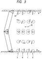
- Alignment states of the type shown in Fig. 2C include four surface stabilization states. Two out of these four states are so-called spray alignment states wherein directors are twisted between the upper and lower substrates. The remaining two states are so-called uniform alignment states wherein directors are almost uniform between the upper and lower substrates. It is presumed that these alignment states correspond to alignment states shown in Fig. 3 under an assumption that directors are present on a cone defined by the helical structure of the smectic C phase. In Fig. 3, a to d represent arrangements of C directors when the cone is viewed from its bottom surface.
- a and b indicate the spray alignment states
- c and d indicate uniform alignment states
- An arrow 31 indicates the direction of spontaneous polarization.
- the uniform alignment states c and d are used in a display element, thereby realizing a high-contrast display.
- the FLC is normally used in the form of a simple matrix display element.
- a voltage equal to or higher than a threshold value is applied to pixels on a selected scanning line to determine an ON or OFF state, and an alternating voltage signal is applied to pixels on a non-selected scanning line.
- image quality is degraded, and the display element cannot withstand long-time use.
- the present invention has been made in consideration of the conventional problems, and has as its object to provide a ferroelectric liquid crystal element, which can prevent image quality from being degraded even when a pre-tilt angle is large.
- a ferroelectric liquid crystal element which is constituted by holding a chiral smectic liquid crystal exhibiting ferroelectricity between electrode substrates, and in which the liquid crystal presents a plurality of surface stabilization states according to an electric field applied through the electrode substrates, and an alternating electric field having a strength equal to or higher than a constant value is applied during a period for inhibiting transition of the surface stabilization state, and to a corresponding liquid crystal portion, within a range causing no transition, wherein the strength of the alternating electric field to be applied during the period for inhibiting transition of the surface stabilization state, and to the corresponding liquid crystal portion is set to be equal to or lower than a predetermined value which does not cause the liquid crystal to flow.
- a liquid crystal for example, if an alternating electric field exceeding a predetermined value is applied to cause the flow of the liquid crystal, the direction of the flow is reversed according to the positive or negative level of the alternating electric field.
- the direction of the flow varies depending on surface stabilization stated.
- the velocity of the flow is low when the direction of the alternating electric field is the same as an average direction of spontaneous polarization of the liquid crystal in an electric field non-application state, and is high when the direction of the alternating electric field is opposite to the average direction.
- a smectic layer of a liquid crystal is, for example, bent, and if the liquid crystal is caused to flow, an average molecular axis direction of the liquid crystal in an electric field application state is present inside an angle defined by a bisector direction of the bent corner, i.e., an outward direction of the bent corner, and the direction of the flow of the liquid crystal.
- a force for causing the flow of the liquid crystal is proportional to the strength of an electric field to be applied, and a force, from an electrode substrate surface, for blocking the flow of the liquid crystal varies depending on a direction to cause the flow.
- the pre-tilt angle of the liquid crystal near the substrate in each stable state varies depending on, e.g., a gap between opposing electrode substrates.
- the opposing electrode substrates have a scanning electrode group for applying an electric field to the liquid crystal, and an information electrode group crossing the scanning electrode group. Each crossing portion forms a pixel.
- an electric field having a strength equal to or higher than a threshold value for causing transition of a surface stabilization state is applied to pixels on the selected scanning electrode, thus transiting the surface stabilization state of the pixels.
- an electric field equal to or higher than a constant value within a range wherein no transition occurs, and equal to or lower than a predetermined value which does not cause the flow of the liquid crystal is applied to pixels on the non-selected scanning electrode.
- the strength of the alternating electric field, which is to be applied during a period for inhibiting transition of the surface stabilization state, and to the corresponding liquid crystal portion, and has a strength equal to or higher than the constant value within the range causing no transition is further limited to be equal to or lower than the predetermined value.
- the present inventors revealed from their experiments that when the pre-tilt angle was large, the liquid crystal flowed in one direction when a drive operation was performed for a long period of time.
- the directions of the flows are parallel to a smectic layer, and are opposite to each other in two uniform stabilization states. Note that polymer alignment films on the opposing surfaces of substrates 21 and 22 are subjected to a rubbing treatment, and these substrates are adhered to each other, so that rubbing directions A of these substrates are parallel to each other.
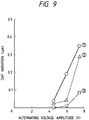
- Fig. 4 is a graph showing results obtained by measuring a state wherein a velocity v of the flow depends on a peak value V of a non-selection application voltage.
- Fig. 5 shows measurement results when other liquid crystal materials A and B were used.
- the electric field strength is similarly plotted along the abscissa.
- the liquid crystals A and B used in the measurement respectively have spontaneous polarization values Ps of -5 nC/cm2 and -3.8 nC/cm2 at 30°C, and respectively have the following phase series characteristics 2 and 3.
- Fig. 6A shows optical response characteristics (transmittance T) in the up state when the alternating voltage shown in Fig. 6A is applied, and Fig. 6C shows optical response characteristics in the down state. Note that Figs.
- FIGS. 6B and 6C show a case wherein a polarization plate (crossed nicols) is arranged at a position where the darkest state is attained in a non-electric field state.
- a polarization plate crossed nicols
- liquid crystal molecules are moved more or less even at the alternating voltages equal to or lower than a threshold value, and as the moving amount is increased, the flow becomes larger.
- the liquid crystal molecules are moved largely upon application of an electric field in a down direction in the up state, and are moved largely in the down state upon application of an electric field having an up direction.
- the liquid crystal molecules are moved in a vibration manner in the flow direction in response to the positive or negative level of an electric field.
- the liquid crystal molecules are moved slightly upon application of the electric field in the same direction as the direction of spontaneous polarization, and are moved largely upon application of the electric field in the opposing direction. As a result, the flow in one direction is generated as a net movement.
- the flow velocity strongly depends on the electric field strength, and the reason why almost no flow occurs at an electric field equal to or lower than a given critical value is not clear yet, but can be considered as follows. More specifically, when a downward electric field equal to or lower than a switching threshold value is applied in the case of the director arrangement in the alignment state c in Fig. 3 (spontaneous polarization is directed upward, i.e., the up state), since C directors having a large pre-tilt angle, and located near the interface are located at a position of a higher phase angle than the edges of cones, a director near the upper substrate is rotated clockwise on the cone, and a director near the lower substrate is rotated counterclockwise.
- the shear stress have opposing directions in upper and lower halves of a chevron, and the liquid crystal receives a force to the left (in a direction of an arrow 32) as a whole.
- the liquid crystal receives a force to the right as a whole.
- an alternating electric field having symmetric positive and negative levels is applied, the liquid crystal continuously receives a force alternating to the right and left. Therefore, when the director is fixed in position, the sign of the shear stress is merely changed in correspondence with a change in sign of the electric field. Therefore, the force based on the upward electric field has the same magnitude as the force based on the downward electric field.
- the liquid crystal is moved to the right and left in the smectic layer. Since the magnitudes of the forces are balanced, it seems that a net flow will not occur. However, when the liquid crystal is moved relative to the substrate, it receives a frictional force from the substrate, and the frictional force must also be taken into consideration. It is considered that the pre-tilt angles of the upper and lower substrate interfaces are not equal to each other, as shown in Fig. 8A since they vary depending on the directions of polarization of the liquid crystal. In this case, forces at which the substrates thrust the liquid crystal must be different from each other at the upper and lower substrate interfaces due to the above-mentioned shear stress.
- both the upper and lower substrates give a thrust to the liquid crystal.
- the difference between the two forces is large, perhaps, the lower substrate interface gives a large thrust, thereby flowing the liquid crystal.
- the liquid crystal is moved relative to the substrate.
- the upper substrate gives, to the liquid crystal, a frictional force opposing the flow rather than a thrust.
- the frictional force is determined by the shape of the substrate surface and the arrangement of interface liquid crystal molecules. Since the interface liquid crystal molecule is asymmetrically arranged in the right and left directions, the right and left magnitudes of a frictional resistance are also different from each other.
- the above discussion has been made about the alignment state c (up state) shown in Fig. 3.
- the down state is established by rotating the up state through 180° about an axis passing through the bending point of a chevron, and perpendicular to the drawing surface of Fig. 3, and has a director arrangement at the substrate interface opposite to that shown in Fig. 8A, as shown in Fig. 8B.
- the shear stress and the frictional force at the interface have the same magnitudes as those in the up state, their directions are reversed.
- the liquid crystal flows in a direction opposite to that in the up state.
- the shear stress that has been described with reference to Figs. 7A and 7B is proportional to the revolution velocity of a molecule, i.e., a moving velocity of a director on the cone. Since the moving velocity of the director on the cone is almost proportional to an electric field strength if an elastic strain is neglected, the shear stress acts more strongly as the electric field strength is increased.
- frictional forces with the substrate include a static frictional force obtained when the liquid crystal at the interface is not moved relative to the substrate, and a dynamic frictional force obtained when the liquid crystal is moved.
- the strength of an alternating electric field to be applied during a period for inhibiting transition of a surface stabilization state, and to a corresponding liquid crystal portion is set to be equal to or smaller than a predetermined value that does not cause the liquid crystal to flow, the cell thickness can be prevented from being changed by the liquid crystal flow even when an identical display state continues for a long period of time. Therefore, good image quality free from degradation can be maintained even if the liquid crystal element is used for a long period of time.
- the predetermined value includes two kinds of values. That is, the first predetermined value is a critical voltage at a constant frequency, and the second predetermined value is a critical voltage under a condition that a frequency is changed together with a voltage, and a selection pulse coincides with a switching threshold value at that frequency.
- Which value is to be used is determined depending on a given drive condition. More specifically, a drive method that has a limitation, i.e., must maintain a constant drive frequency, employs the first critical voltage. This case corresponds to an application to, e.g., a display such as a television. In contrast to this, in a display device having no limitation on a drive frequency, it is proper to set the second critical voltage or less while decreasing a frequency as much as possible. In the case of a display device of a computer terminal, data communications with a main body computer are adjusted, so that the display device is not always driven at a TV rate. The latter case corresponds to this application.
- FIG. 10 shows an example of the present invention.
- a system shown in Fig. 10 includes a graphic controller 107, a drive control circuit 105, a scanning signal control circuit 104, an information signal control circuit 106, a scanning signal application circuit 102, an information signal application circuit 103, and a liquid crystal display 101.
- Data and a scanning form signal sent from the graphic controller 107 are input to the drive control circuit 104 and the information signal control circuit 106.
- the data is converted into address data and display data, and the scanning form signal is supplied directly to the scanning signal application circuit 102 and the information signal application circuit 103.
- the scanning signal application circuit 102 applies a scanning signal waveform determined by the scanning form signal to a scanning electrode determined by the address data.
- the information signal application circuit 103 applies an information signal waveform determined by a black or white display content input as the display data, and the scanning form signal.
- Fig. 11 is an enlarged view of the liquid crystal display 101.
- the liquid crystal display shown in Fig. 11 includes scanning electrodes C1 to C6, and information electrodes S1 to S6, which are arranged to form a matrix.
- a pixel P22 serving as a display unit is defined by the scanning and information electrodes.
- Fig. 12 is a sectional view including the scanning electrode C2 shown in Fig. 11.
- the liquid crystal display shown in Fig. 12 includes an analyzer 301 and a polarizer 305, which are arranged in a "crossed nicols" manner.
- the liquid crystal display also includes glass substrates 302 and 304, a ferroelectric liquid crystal 303, and a spacer 306.
- Substrates on each of which a polyimide film (not shown; LQ1802 available from Hitachi Kasei (KK)) was formed on the electrodes as an alignment film, were subjected to rubbing using nylon cloth, and were adhered to each other, so that the rubbing directions of the upper and lower substrates were shifted by 6° in a clockwise direction, thus preparing a cell.
- the cell thickness was 1.3 ⁇ m.
- the above-mentioned liquid crystal A having the spontaneous polarization value Ps of -5.6 nC/cm2 at 30°C, and the above-mentioned phase change characteristics was injected into the cell, and was cooled to be set in an SC* phase, thus forming an SSFLC state.
- a pulse electric field was then applied to the entire cell to align the overall cell in one stable state.
- a rectangular wave alternating electric field having an electric field strength of ⁇ 3 V/ ⁇ m and a frequency of 12.5 kHz was kept applied to the cell. As a result, almost no change in display state was observed even after an elapse of two days.
- Substrates subjected to the same alignment treatment as the above cell were adhered to each other, so that their rubbing directions were anti-parallel to each other, and another liquid crystal was injected into a gap between the substrates.
- a pre-tilt angle was then measured by a crystal rotation method. The angle was about 17°.
- Figs. 4 and 5, and Example 1 have discussed the electric field strength dependency of a flow velocity at a constant frequency (12.5 kHz).
- a threshold value is normally applied during a non-selection period wherein a display state is left unchanged, and to a corresponding area.
- the amplitude of the non-selection voltage is plotted along the abscissa.
- a frequency is changed accordingly, so that a selection pulse can coincide with a threshold value.
- Different frequencies are employed depending on types of liquid crystals. For example, in the case of the liquid crystal exhibiting the phase series characteristics 1, frequencies of 5.6 kHz, 8.2 kHz, and 11.1 kHz are used. As can be apparent from Fig. 11, the electric field dependency of a flow velocity in this case also has critical characteristics, and almost no flow was generated at 4.5 V or less.
- a ferroelectric liquid crystal element which is constituted by holding a chiral smectic liquid crystal exhibiting ferroelectricity between electrode substrates, and in which the liquid crystal presents a plurality of surface stabilization states according to an electric field applied through the electrode substrates, and an alternating electric field having a strength equal to or higher than a constant value is applied during a period for inhibiting transition of the surface stabilization state, and to a corresponding liquid crystal portion, within a range causing no transition, the strength of the alternating electric field to be applied during the period for inhibiting transition of the surface stabilization state, and to the corresponding liquid crystal portion is set to be equal to or lower than a predetermined value which does not cause the liquid crystal to flow.
Applications Claiming Priority (2)
| Application Number | Priority Date | Filing Date | Title |
|---|---|---|---|
| JP11529/91 | 1991-01-08 | ||
| JP3011529A JP2802685B2 (ja) | 1991-01-08 | 1991-01-08 | 強誘電性液晶装置 |
Publications (3)
| Publication Number | Publication Date |
|---|---|
| EP0494626A2 true EP0494626A2 (de) | 1992-07-15 |
| EP0494626A3 EP0494626A3 (en) | 1993-01-13 |
| EP0494626B1 EP0494626B1 (de) | 1999-04-21 |
Family
ID=11780498
Family Applications (1)
| Application Number | Title | Priority Date | Filing Date |
|---|---|---|---|
| EP92100126A Expired - Lifetime EP0494626B1 (de) | 1991-01-08 | 1992-01-07 | Ferroelektrisches Flüssigkristallelement |
Country Status (5)
| Country | Link |
|---|---|
| US (2) | US5500749A (de) |
| EP (1) | EP0494626B1 (de) |
| JP (1) | JP2802685B2 (de) |
| AT (1) | ATE179260T1 (de) |
| DE (1) | DE69228956T2 (de) |
Cited By (4)
| Publication number | Priority date | Publication date | Assignee | Title |
|---|---|---|---|---|
| EP0550846A1 (de) * | 1991-12-10 | 1993-07-14 | Canon Kabushiki Kaisha | Ferroelektrische Flüssigkristall-Anzeigevorrichtung und Verfahren zu ihrer Herstellung |
| EP0553727A2 (de) * | 1992-01-24 | 1993-08-04 | Canon Kabushiki Kaisha | Ferroelektrische Flüssigkristallvorrichtung und Verfahren zur Behandlung derselben |
| US5594571A (en) * | 1991-12-10 | 1997-01-14 | Canon Kabushiki Kaisha | Ferroelectric liquid crystal device and process for production thereof |
| GB2314169A (en) * | 1996-06-11 | 1997-12-17 | Sharp Kk | Ferroelectric liquid crystal device alignment |
Families Citing this family (14)
| Publication number | Priority date | Publication date | Assignee | Title |
|---|---|---|---|---|
| US5815230A (en) * | 1994-01-27 | 1998-09-29 | Canon Kabushiki Kaisha | Liquid crystal device and process for production thereof |
| JPH07287232A (ja) * | 1994-04-18 | 1995-10-31 | Fujitsu Ltd | 液晶表示装置、その製造方法、および駆動方法 |
| GB2293906A (en) * | 1994-10-03 | 1996-04-10 | Sharp Kk | Liquid crystal display |
| JP3669708B2 (ja) * | 1995-07-03 | 2005-07-13 | シチズン時計株式会社 | 液晶表示装置 |
| US5764328A (en) * | 1995-07-03 | 1998-06-09 | Citizen Watch Co., Ltd. | Liquid crystal device with plural ferroelectric or antiferroelectric layer tilt angles per pixel |
| JPH09146126A (ja) * | 1995-11-22 | 1997-06-06 | Canon Inc | 液晶装置及び情報伝達装置 |
| US6020947A (en) * | 1996-11-06 | 2000-02-01 | Sharp Kabushiki Kaisha | Liquid crystal devices |
| JPH1124041A (ja) * | 1997-06-30 | 1999-01-29 | Toshiba Corp | 液晶表示装置 |
| NO309500B1 (no) | 1997-08-15 | 2001-02-05 | Thin Film Electronics Asa | Ferroelektrisk databehandlingsinnretning, fremgangsmåter til dens fremstilling og utlesing, samt bruk av samme |
| JP3559719B2 (ja) | 1998-01-13 | 2004-09-02 | キヤノン株式会社 | プラズマアドレス型の液晶表示装置 |
| JP3323847B2 (ja) * | 1999-02-22 | 2002-09-09 | キヤノン株式会社 | 電子放出素子、電子源および画像形成装置の製造方法 |
| JP2001291594A (ja) | 2000-04-07 | 2001-10-19 | Canon Inc | 導電性液晶素子 |
| JP5121432B2 (ja) * | 2007-12-11 | 2013-01-16 | キヤノン株式会社 | 液晶表示装置及びその製造方法並びに液晶プロジェクション装置 |
| CN103293734B (zh) * | 2012-08-27 | 2015-12-02 | 上海天马微电子有限公司 | 内嵌式触控显示装置 |
Family Cites Families (28)
| Publication number | Priority date | Publication date | Assignee | Title |
|---|---|---|---|---|
| US4813767A (en) * | 1980-01-08 | 1989-03-21 | Clark Noel A | Surface stabilized ferroelectric liquid crystal devices |
| JPS6033535A (ja) * | 1983-08-04 | 1985-02-20 | Canon Inc | 液晶装置 |
| US4715688A (en) * | 1984-07-04 | 1987-12-29 | Seiko Instruments Inc. | Ferroelectric liquid crystal display device having an A.C. holding voltage |
| US4682858A (en) * | 1984-08-20 | 1987-07-28 | Canon Kabushiki Kaisha | Liquid crystal device having reduced-pressure region in communication with ferroelectric liquid crystal |
| US4923285A (en) * | 1985-04-22 | 1990-05-08 | Canon Kabushiki Kaisha | Drive apparatus having a temperature detector |
| US4898456A (en) * | 1985-04-23 | 1990-02-06 | Canon Kabushiki Kaisha | Liquid crystal optical device |
| FR2581209B1 (fr) * | 1985-04-26 | 1993-11-05 | Canon Kk | Dispositif optique a cristal liquide |
| US4844590A (en) * | 1985-05-25 | 1989-07-04 | Canon Kabushiki Kaisha | Method and apparatus for driving ferroelectric liquid crystal device |
| US4778259A (en) * | 1985-07-17 | 1988-10-18 | Canon Kabushiki Kaisha | Ferroelectric liquid crystal devices having reverse twist angle and stable states resulting from A.C. excitation |
| DE3630012A1 (de) * | 1985-09-04 | 1987-04-23 | Canon Kk | Ferroelektrische fluessigkristallvorrichtung |
| US4879059A (en) * | 1986-09-02 | 1989-11-07 | Canon Kabushiki Kaisha | Liquid crystal device |
| JPS6373228A (ja) * | 1986-09-17 | 1988-04-02 | Canon Inc | 光学変調素子の駆動法 |
| US5182549A (en) * | 1987-03-05 | 1993-01-26 | Canon Kabushiki Kaisha | Liquid crystal apparatus |
| US4900132A (en) * | 1987-04-13 | 1990-02-13 | Tektronix, Inc. | Chiral liquid crystal cell |
| US4932758A (en) * | 1987-09-17 | 1990-06-12 | Canon Kabushiki Kaisha | Ferroelectric smectic liquid crystal device having a bistable alignment state providing two stable orientation states |
| JPS6477022A (en) * | 1987-09-18 | 1989-03-23 | Canon Kk | Ferroelectric liquid crystal element |
| JPH02125227A (ja) * | 1988-11-04 | 1990-05-14 | Seiko Epson Corp | 液晶素子の駆動方法 |
| JP2816403B2 (ja) * | 1988-11-11 | 1998-10-27 | 株式会社 半導体エネルギー研究所 | 液晶表示装置の駆動方法および液晶表示装置 |
| JP2660566B2 (ja) * | 1988-12-15 | 1997-10-08 | キヤノン株式会社 | 強誘電性液晶装置およびその駆動法 |
| JP2549433B2 (ja) * | 1989-03-13 | 1996-10-30 | 株式会社日立製作所 | 電気光学変調素子の駆動方法およびプリンタ |
| US5267065A (en) * | 1989-04-24 | 1993-11-30 | Canon Kabushiki Kaisha | Liquid crystal apparatus |
| NL8901481A (nl) * | 1989-06-12 | 1991-01-02 | Philips Nv | Passieve ferro-elektrisch vloeibaar kristal weergeefinrichting en werkwijze ter vervaardiging daarvan. |
| EP0444705B1 (de) * | 1990-03-02 | 1999-05-26 | Canon Kabushiki Kaisha | Flüssigkristallelement und Flüssigkristallvorrichtung, die dieses Element verwendet |
| JP2915104B2 (ja) * | 1990-07-30 | 1999-07-05 | キヤノン株式会社 | 液晶素子および液晶駆動方法 |
| JP3227197B2 (ja) * | 1991-06-18 | 2001-11-12 | キヤノン株式会社 | 表示装置 |
| JP2954429B2 (ja) * | 1992-08-25 | 1999-09-27 | シャープ株式会社 | アクティブマトリクス方式駆動装置 |
| US5583534A (en) * | 1993-02-18 | 1996-12-10 | Canon Kabushiki Kaisha | Method and apparatus for driving liquid crystal display having memory effect |
| US5532713A (en) * | 1993-04-20 | 1996-07-02 | Canon Kabushiki Kaisha | Driving method for liquid crystal device |
-
1991
- 1991-01-08 JP JP3011529A patent/JP2802685B2/ja not_active Expired - Fee Related
-
1992
- 1992-01-07 EP EP92100126A patent/EP0494626B1/de not_active Expired - Lifetime
- 1992-01-07 AT AT92100126T patent/ATE179260T1/de not_active IP Right Cessation
- 1992-01-07 DE DE69228956T patent/DE69228956T2/de not_active Expired - Fee Related
-
1994
- 1994-07-26 US US08/280,583 patent/US5500749A/en not_active Expired - Fee Related
-
1995
- 1995-12-06 US US08/568,298 patent/US5805129A/en not_active Expired - Fee Related
Non-Patent Citations (2)
| Title |
|---|
| FERROELECTRICS. vol. 69, no. 3/4, 1986, LONDON GB pages 153 - 163 A. JÁKLI ET AL. 'Electromechanical Effect in SC* Liquid Crystals' * |
| SID 1985 DIGEST OF TECHNICAL PAPERS, US pages 128 - 130 J.M. GEARY 'A Multiplexed Ferroelectric LCD Using AC Field-Stabilized States' * |
Cited By (13)
| Publication number | Priority date | Publication date | Assignee | Title |
|---|---|---|---|---|
| US5764327A (en) * | 1991-12-10 | 1998-06-09 | Canon Kabushiki Kaisha | Ferroelectric liquid crystal device with uneven surface under alignment film and process for production |
| US5381256A (en) * | 1991-12-10 | 1995-01-10 | Canon Kabushiki Kaisha | Ferroelectric liquid crystal device with fine particles on insulator, having diameter less than substrate gap |
| EP0703484A1 (de) * | 1991-12-10 | 1996-03-27 | Canon Kabushiki Kaisha | Ferroelektrische Flüssigkristallvorrichtung und Verfahren zu ihrer Herstellung |
| EP0703483A1 (de) * | 1991-12-10 | 1996-03-27 | Canon Kabushiki Kaisha | Ferroelektrische Flüssigkristallvorrichtung und Verfahren zu ihrer Herstellung |
| US5594571A (en) * | 1991-12-10 | 1997-01-14 | Canon Kabushiki Kaisha | Ferroelectric liquid crystal device and process for production thereof |
| EP0550846A1 (de) * | 1991-12-10 | 1993-07-14 | Canon Kabushiki Kaisha | Ferroelektrische Flüssigkristall-Anzeigevorrichtung und Verfahren zu ihrer Herstellung |
| US5835248A (en) * | 1991-12-10 | 1998-11-10 | Canon Kabushiki Kaisha | Method of making ferroelectric liquid crystal device using particles to create an unevenness on alignment layer or underlying insulating layer |
| EP0553727A2 (de) * | 1992-01-24 | 1993-08-04 | Canon Kabushiki Kaisha | Ferroelektrische Flüssigkristallvorrichtung und Verfahren zur Behandlung derselben |
| EP0553727A3 (en) * | 1992-01-24 | 1993-11-03 | Canon Kk | Ferroelectric liquid crystal device and treatment method therefor |
| US5543943A (en) * | 1992-01-24 | 1996-08-06 | Canon Kabushiki Kaisha | Chiral smectic device subjected to a simultaneous thermal and AC field treatment |
| US5790223A (en) * | 1992-01-24 | 1998-08-04 | Canon Kabushiki Kaisha | Ferroelectric liquid crystal device and treatment method therefor |
| GB2314169A (en) * | 1996-06-11 | 1997-12-17 | Sharp Kk | Ferroelectric liquid crystal device alignment |
| GB2314169B (en) * | 1996-06-11 | 2000-02-16 | Sharp Kk | Ferroelectric liquid crystal device alignment |
Also Published As
| Publication number | Publication date |
|---|---|
| US5500749A (en) | 1996-03-19 |
| JPH04251218A (ja) | 1992-09-07 |
| US5805129A (en) | 1998-09-08 |
| EP0494626B1 (de) | 1999-04-21 |
| DE69228956D1 (de) | 1999-05-27 |
| DE69228956T2 (de) | 1999-12-02 |
| JP2802685B2 (ja) | 1998-09-24 |
| ATE179260T1 (de) | 1999-05-15 |
| EP0494626A3 (en) | 1993-01-13 |
Similar Documents
| Publication | Publication Date | Title |
|---|---|---|
| US5805129A (en) | Inhibiting transition of a surface stabilization state in a ferroelectric liquid crystal element using alternating voltages | |
| US4738515A (en) | Driving method for liquid crystal device | |
| AU634031B2 (en) | Liquid crystal element and liquid crystal apparatus using the same | |
| US6037920A (en) | Liquid crystal apparatus and driving method therefor | |
| KR0138968B1 (ko) | 전기광학장치 | |
| US6108061A (en) | Liquid crystal element stabilized by the use of polymer reticulate structure, and manufacturing method thereof | |
| EP0542518B1 (de) | Flüssigkristallelement und Steuerverfahren dafür | |
| US4917470A (en) | Driving method for liquid crystal cell and liquid crystal apparatus | |
| US5136408A (en) | Liquid crystal apparatus and driving method therefor | |
| US5276542A (en) | Ferroelectric liquid crystal apparatus having temperature compensation control circuit | |
| US5541752A (en) | Liquid crystal apparatus | |
| US5999157A (en) | Suppressing liquid crystal movement based on the relationship between a display pattern and a driving waveform | |
| US20020191137A1 (en) | Liquid crystal panel substrate having alignment film and method for forming alignment film | |
| Koden et al. | Ferroelectric liquid crystal device using the τ-VMIN mode | |
| JP2525453B2 (ja) | 液晶装置及びその駆動法 | |
| US5943035A (en) | Driving method and apparatus for liquid crystal device | |
| Koden et al. | Ferroelectric liquid crystal display | |
| Kondo et al. | Threshold Behavior of a Bistable Ferroelectric Liquid Crystal with a Large Tilt Angle in Thick Cells (4-14µm) | |
| JPH0792562B2 (ja) | 液晶表示装置の駆動方法 | |
| JPH06194623A (ja) | 反強誘電性液晶表示素子の駆動方法 | |
| Wakita et al. | AC-field-stabilized matrix ferroelectric LCD | |
| CA1304485C (en) | Liquid crystal display element and method for driving same | |
| JP3219709B2 (ja) | 液晶素子、液晶装置、及び液晶素子の駆動方法 | |
| JPH1054976A (ja) | 液晶表示装置ならびにその駆動回路および駆動方法 | |
| JPS63210825A (ja) | 光スイツチの駆動方法 |
Legal Events
| Date | Code | Title | Description |
|---|---|---|---|
| PUAI | Public reference made under article 153(3) epc to a published international application that has entered the european phase |
Free format text: ORIGINAL CODE: 0009012 |
|
| AK | Designated contracting states |
Kind code of ref document: A2 Designated state(s): AT BE CH DE DK ES FR GB GR IT LI LU NL SE |
|
| PUAL | Search report despatched |
Free format text: ORIGINAL CODE: 0009013 |
|
| AK | Designated contracting states |
Kind code of ref document: A3 Designated state(s): AT BE CH DE DK ES FR GB GR IT LI LU NL SE |
|
| 17P | Request for examination filed |
Effective date: 19930524 |
|
| 17Q | First examination report despatched |
Effective date: 19950529 |
|
| GRAG | Despatch of communication of intention to grant |
Free format text: ORIGINAL CODE: EPIDOS AGRA |
|
| GRAG | Despatch of communication of intention to grant |
Free format text: ORIGINAL CODE: EPIDOS AGRA |
|
| GRAH | Despatch of communication of intention to grant a patent |
Free format text: ORIGINAL CODE: EPIDOS IGRA |
|
| GRAH | Despatch of communication of intention to grant a patent |
Free format text: ORIGINAL CODE: EPIDOS IGRA |
|
| GRAA | (expected) grant |
Free format text: ORIGINAL CODE: 0009210 |
|
| AK | Designated contracting states |
Kind code of ref document: B1 Designated state(s): AT BE CH DE DK ES FR GB GR IT LI LU NL SE |
|
| PG25 | Lapsed in a contracting state [announced via postgrant information from national office to epo] |
Ref country code: IT Free format text: LAPSE BECAUSE OF FAILURE TO SUBMIT A TRANSLATION OF THE DESCRIPTION OR TO PAY THE FEE WITHIN THE PRESCRIBED TIME-LIMIT;WARNING: LAPSES OF ITALIAN PATENTS WITH EFFECTIVE DATE BEFORE 2007 MAY HAVE OCCURRED AT ANY TIME BEFORE 2007. THE CORRECT EFFECTIVE DATE MAY BE DIFFERENT FROM THE ONE RECORDED. Effective date: 19990421 Ref country code: BE Free format text: LAPSE BECAUSE OF FAILURE TO SUBMIT A TRANSLATION OF THE DESCRIPTION OR TO PAY THE FEE WITHIN THE PRESCRIBED TIME-LIMIT Effective date: 19990421 Ref country code: LI Free format text: LAPSE BECAUSE OF FAILURE TO SUBMIT A TRANSLATION OF THE DESCRIPTION OR TO PAY THE FEE WITHIN THE PRESCRIBED TIME-LIMIT Effective date: 19990421 Ref country code: NL Free format text: LAPSE BECAUSE OF FAILURE TO SUBMIT A TRANSLATION OF THE DESCRIPTION OR TO PAY THE FEE WITHIN THE PRESCRIBED TIME-LIMIT Effective date: 19990421 Ref country code: ES Free format text: THE PATENT HAS BEEN ANNULLED BY A DECISION OF A NATIONAL AUTHORITY Effective date: 19990421 Ref country code: GR Free format text: LAPSE BECAUSE OF NON-PAYMENT OF DUE FEES Effective date: 19990421 Ref country code: CH Free format text: LAPSE BECAUSE OF FAILURE TO SUBMIT A TRANSLATION OF THE DESCRIPTION OR TO PAY THE FEE WITHIN THE PRESCRIBED TIME-LIMIT Effective date: 19990421 Ref country code: AT Free format text: LAPSE BECAUSE OF FAILURE TO SUBMIT A TRANSLATION OF THE DESCRIPTION OR TO PAY THE FEE WITHIN THE PRESCRIBED TIME-LIMIT Effective date: 19990421 Ref country code: SE Free format text: THE PATENT HAS BEEN ANNULLED BY A DECISION OF A NATIONAL AUTHORITY Effective date: 19990421 |
|
| REF | Corresponds to: |
Ref document number: 179260 Country of ref document: AT Date of ref document: 19990515 Kind code of ref document: T |
|
| REG | Reference to a national code |
Ref country code: CH Ref legal event code: EP |
|
| REF | Corresponds to: |
Ref document number: 69228956 Country of ref document: DE Date of ref document: 19990527 |
|
| ET | Fr: translation filed | ||
| PG25 | Lapsed in a contracting state [announced via postgrant information from national office to epo] |
Ref country code: DK Free format text: LAPSE BECAUSE OF FAILURE TO SUBMIT A TRANSLATION OF THE DESCRIPTION OR TO PAY THE FEE WITHIN THE PRESCRIBED TIME-LIMIT Effective date: 19990721 |
|
| REG | Reference to a national code |
Ref country code: CH Ref legal event code: PL |
|
| PG25 | Lapsed in a contracting state [announced via postgrant information from national office to epo] |
Ref country code: LU Free format text: LAPSE BECAUSE OF NON-PAYMENT OF DUE FEES Effective date: 20000107 |
|
| PLBE | No opposition filed within time limit |
Free format text: ORIGINAL CODE: 0009261 |
|
| STAA | Information on the status of an ep patent application or granted ep patent |
Free format text: STATUS: NO OPPOSITION FILED WITHIN TIME LIMIT |
|
| 26N | No opposition filed | ||
| REG | Reference to a national code |
Ref country code: GB Ref legal event code: IF02 |
|
| PGFP | Annual fee paid to national office [announced via postgrant information from national office to epo] |
Ref country code: GB Payment date: 20021231 Year of fee payment: 12 |
|
| PGFP | Annual fee paid to national office [announced via postgrant information from national office to epo] |
Ref country code: FR Payment date: 20030110 Year of fee payment: 12 |
|
| PGFP | Annual fee paid to national office [announced via postgrant information from national office to epo] |
Ref country code: DE Payment date: 20030116 Year of fee payment: 12 |
|
| PG25 | Lapsed in a contracting state [announced via postgrant information from national office to epo] |
Ref country code: GB Free format text: LAPSE BECAUSE OF NON-PAYMENT OF DUE FEES Effective date: 20040107 |
|
| PG25 | Lapsed in a contracting state [announced via postgrant information from national office to epo] |
Ref country code: DE Free format text: LAPSE BECAUSE OF NON-PAYMENT OF DUE FEES Effective date: 20040803 |
|
| GBPC | Gb: european patent ceased through non-payment of renewal fee |
Effective date: 20040107 |
|
| PG25 | Lapsed in a contracting state [announced via postgrant information from national office to epo] |
Ref country code: FR Free format text: LAPSE BECAUSE OF NON-PAYMENT OF DUE FEES Effective date: 20040930 |
|
| REG | Reference to a national code |
Ref country code: FR Ref legal event code: ST |