EP0487114A2 - Photovoltaisches Bauelement mit Pin-Übergang, mit einer i-Typ Halbleiter-Schicht bestehend aus einer Mehrzahl von Gebieten mit verschiedenen, gradierten Energiebandabständen - Google Patents
Photovoltaisches Bauelement mit Pin-Übergang, mit einer i-Typ Halbleiter-Schicht bestehend aus einer Mehrzahl von Gebieten mit verschiedenen, gradierten Energiebandabständen Download PDFInfo
- Publication number
- EP0487114A2 EP0487114A2 EP91120051A EP91120051A EP0487114A2 EP 0487114 A2 EP0487114 A2 EP 0487114A2 EP 91120051 A EP91120051 A EP 91120051A EP 91120051 A EP91120051 A EP 91120051A EP 0487114 A2 EP0487114 A2 EP 0487114A2
- Authority
- EP
- European Patent Office
- Prior art keywords
- semiconductor layer
- type semiconductor
- band gap
- solar cell
- region
- Prior art date
- Legal status (The legal status is an assumption and is not a legal conclusion. Google has not performed a legal analysis and makes no representation as to the accuracy of the status listed.)
- Granted
Links
Images


Classifications
-
- H—ELECTRICITY
- H10—SEMICONDUCTOR DEVICES; ELECTRIC SOLID-STATE DEVICES NOT OTHERWISE PROVIDED FOR
- H10F—INORGANIC SEMICONDUCTOR DEVICES SENSITIVE TO INFRARED RADIATION, LIGHT, ELECTROMAGNETIC RADIATION OF SHORTER WAVELENGTH OR CORPUSCULAR RADIATION
- H10F10/00—Individual photovoltaic cells, e.g. solar cells
- H10F10/10—Individual photovoltaic cells, e.g. solar cells having potential barriers
- H10F10/13—Photovoltaic cells having absorbing layers comprising graded bandgaps
-
- H—ELECTRICITY
- H10—SEMICONDUCTOR DEVICES; ELECTRIC SOLID-STATE DEVICES NOT OTHERWISE PROVIDED FOR
- H10F—INORGANIC SEMICONDUCTOR DEVICES SENSITIVE TO INFRARED RADIATION, LIGHT, ELECTROMAGNETIC RADIATION OF SHORTER WAVELENGTH OR CORPUSCULAR RADIATION
- H10F10/00—Individual photovoltaic cells, e.g. solar cells
- H10F10/10—Individual photovoltaic cells, e.g. solar cells having potential barriers
- H10F10/17—Photovoltaic cells having only PIN junction potential barriers
- H10F10/172—Photovoltaic cells having only PIN junction potential barriers comprising multiple PIN junctions, e.g. tandem cells
-
- H—ELECTRICITY
- H10—SEMICONDUCTOR DEVICES; ELECTRIC SOLID-STATE DEVICES NOT OTHERWISE PROVIDED FOR
- H10F—INORGANIC SEMICONDUCTOR DEVICES SENSITIVE TO INFRARED RADIATION, LIGHT, ELECTROMAGNETIC RADIATION OF SHORTER WAVELENGTH OR CORPUSCULAR RADIATION
- H10F71/00—Manufacture or treatment of devices covered by this subclass
- H10F71/10—Manufacture or treatment of devices covered by this subclass the devices comprising amorphous semiconductor material
- H10F71/103—Manufacture or treatment of devices covered by this subclass the devices comprising amorphous semiconductor material including only Group IV materials
- H10F71/1035—Manufacture or treatment of devices covered by this subclass the devices comprising amorphous semiconductor material including only Group IV materials having multiple Group IV elements, e.g. SiGe or SiC
-
- H—ELECTRICITY
- H10—SEMICONDUCTOR DEVICES; ELECTRIC SOLID-STATE DEVICES NOT OTHERWISE PROVIDED FOR
- H10F—INORGANIC SEMICONDUCTOR DEVICES SENSITIVE TO INFRARED RADIATION, LIGHT, ELECTROMAGNETIC RADIATION OF SHORTER WAVELENGTH OR CORPUSCULAR RADIATION
- H10F77/00—Constructional details of devices covered by this subclass
- H10F77/10—Semiconductor bodies
- H10F77/14—Shape of semiconductor bodies; Shapes, relative sizes or dispositions of semiconductor regions within semiconductor bodies
-
- Y—GENERAL TAGGING OF NEW TECHNOLOGICAL DEVELOPMENTS; GENERAL TAGGING OF CROSS-SECTIONAL TECHNOLOGIES SPANNING OVER SEVERAL SECTIONS OF THE IPC; TECHNICAL SUBJECTS COVERED BY FORMER USPC CROSS-REFERENCE ART COLLECTIONS [XRACs] AND DIGESTS
- Y02—TECHNOLOGIES OR APPLICATIONS FOR MITIGATION OR ADAPTATION AGAINST CLIMATE CHANGE
- Y02E—REDUCTION OF GREENHOUSE GAS [GHG] EMISSIONS, RELATED TO ENERGY GENERATION, TRANSMISSION OR DISTRIBUTION
- Y02E10/00—Energy generation through renewable energy sources
- Y02E10/50—Photovoltaic [PV] energy
- Y02E10/548—Amorphous silicon PV cells
-
- Y—GENERAL TAGGING OF NEW TECHNOLOGICAL DEVELOPMENTS; GENERAL TAGGING OF CROSS-SECTIONAL TECHNOLOGIES SPANNING OVER SEVERAL SECTIONS OF THE IPC; TECHNICAL SUBJECTS COVERED BY FORMER USPC CROSS-REFERENCE ART COLLECTIONS [XRACs] AND DIGESTS
- Y02—TECHNOLOGIES OR APPLICATIONS FOR MITIGATION OR ADAPTATION AGAINST CLIMATE CHANGE
- Y02P—CLIMATE CHANGE MITIGATION TECHNOLOGIES IN THE PRODUCTION OR PROCESSING OF GOODS
- Y02P70/00—Climate change mitigation technologies in the production process for final industrial or consumer products
- Y02P70/50—Manufacturing or production processes characterised by the final manufactured product
Definitions
- the present invention relates to an improved pin junction photovoltaic element which exhibits an improved photoelectric conversion efficiency and which can be provided at a reduced cost. More particularly, the present invention relates to an improved pin junction photovoltaic element provided with a specific i-type semiconductor layer with a plurality of regions having different graded band gaps which exhibits an improved photoelectric conversion efficiency and which can be provided at a reduced cost.
- solar cells there are a number of solar cells which have been putted in practical use.
- a solar cell made of a single crystal silicon material which is commonly called “single crystal silicon solar cell”
- This single crystal silicon solar cell has been evaluated as being highly reliable and high in photoelectric conversion efficiency.
- This single crystal silicon solar cell is produced in a manner similar to the semiconductor wafer process of producing an integrated circuit.
- a single crystal silicon incorporated with a minute amount of a dopant (valence electron controlling agent in other words) of p-type or n-type is firstly prepare by a crystal growth method, a silicon wafer is quarried from the resultant, and a pn junction is formed in the silicon wafer thus obtained by diffusing a different dopant therein.
- a dopant valence electron controlling agent in other words
- the single crystal silicon solar cell light such as sunlight is absorbed, the light absorbed is excited to generate photocarriers, those photocarriers are migrated by the action of internal electric field of the pn junction, whereby a photoelectromotive force is outputted.
- the single crystal silicon solar cell is costly since it is produced by way of such semiconductor wafer process as above mentioned.
- the single crystal silicon solar cell there is a limit for the area of a silicon wafer to be produced because of single crystal and it is therefore extremely difficult to make it to be of a large area.
- the single crystal silicon solar cell in order for the single crystal silicon solar cell to be a module usable as a power source in outdoors, it is necessary to be provided with a relevant protective equipment. In consequence, the resulting single crystal silicon solar cell module unavoidably becomes such that is relatively costly in comparison with oil fired power generation in terms of production cost of a unit electricity.
- non-single crystal semiconductor films such as tetrahedral non-single crystal semiconductor films of amorphous silicon (a-Si), amorphous silicon germanium (a-SiGe), amorphous silicon carbide (a-SiC), etc., compound semiconductor films containing elements of the groups II and VI of the periodic table such as CdS, CdTe, Cu2S, ZnSe and ZnTe semiconductor films, and other compound semiconductor films containing elements of the groups I, III and VI of the periodic table.
- a-Si amorphous silicon
- a-SiGe amorphous silicon germanium
- a-SiC amorphous silicon carbide
- the tetrahedral non-single crystal semiconductor films (that is, amorphous silicon semiconductor films) are expected to be the most promising in view of their various advantages that a large semiconductor film capable of being the constituent of a solar cell can be relatively easily formed; said semiconductor film can be thinned as desired; said semiconductor film can be formed on an optional substrate; a large area solar cell can be produced on an industrial scale; and thus, it is possible to provide a solar cell at a reasonable cost.
- non-single crystal solar cells amorphous semiconductor films
- MIS type comprising metal layer/insulating layer/semiconductor layer
- heterojunction type a type of solar cells of pin junction type
- the pin junction solar cell is typically of the constitution that comprises an electrode, a metallic layer and a photoelectromotive force generating layer, and another electrode being disposed in this order on a substrate, in which said photoelectromotive force generating layer comprises a multilayered body comprising an n-type semiconductor layer, an i-type semiconductor layer and a p-type semiconductor layer.
- amorphous silicon which is the most widely used at the present time as an amorphous semiconductor
- its energy band width is about 1.7 or more, and because of this, light of 750 nm or more in wavelength is hardly absorbed by the amorphous silicon. Therefore, long wavelength energy components of sunlight spectra are not efficiently utilized in the case of an amorphous silicon solar cell.
- silicon-containing amorphous materials comprising a-Si incorporated with appropriate atoms such as germanium atoms (Ge), tin atoms (Sn) or lead atoms (Pb) which have a band gap narrower than that of the a-Si (amorphous silicon).
- germanium atoms Ge
- tin atoms Sn
- Pb lead atoms
- pin junction solar cell which is a so-called single cell type pin junction solar cell
- a multicells-stacked solar cell comprising a pin junction solar cell element having an i-type semiconductor layer formed of such narrow band gap silicon-containing amorphous material and other pin junction solar cell element having an i-type semiconductor layer formed of a-Si being stacked. It is generally believed that the latter multicells-stacked solar cell provides a photoelectric conversion efficiency greater than that provided by the former single cell type solar cell.
- U.S. Patent No. 4,816,082 (hereinafter referred to as "Literature 1”) proposes a pin junction solar cell having an i-type semiconductor layer comprising an amorphous alloy in which the band gap of the i-type semiconductor layer is graded such that the band gap of each of the regions in contact with the p-type semiconductor layer and the n-type semiconductor layer is widened and it is minimum at a given region.
- This proposed pin junction solar cell aims at providing an improved photoelectric conversion efficiency by varying the band gap of the i-type semiconductor layer depending on the position thereof in the thickness direction.
- U.S. Patent No. 4,542,256 (hereinafter referred to as "Literature 2”) proposes a pin junction photovoltaic cell (namely, pin junction solar cell) which is aimed at providing an improved photoelectric conversion efficiency by forming the n-type semiconductor layer or the p-type semiconductor layer of a material having a band gap wider than that of the constituent material of the i-type semiconductor layer and disposing a layer (that is a so-called intermediate layer) having a continuously graded band gap not only at the interface between the p-type semiconductor layer and the i-type semiconductor layer but also at the interface between the n-type semiconductor layer and the i-type semiconductor layer.
- a layer that is a so-called intermediate layer
- the principal object of the present invention is to provide an improved photovoltaic element which exhibits an fill factor higher than that in the case of the known photovoltaic element and provides a satisfactory photoelectric conversion efficiency.
- Another object of the present invention is to provide an improved photovoltaic element having an i-type semiconductor layer formed of a band gap variable semiconductor material between a p-type semiconductor layer having a band gap wider than that of said i-type semiconductor layer and an n-type semiconductor layer having a band gap wider than that of said i-type semiconductor layer, characterized in that said i-type semiconductor layer contains (a) a first region which is positioned on the side of said p-type semiconductor layer and has a graded band gap, (b) a second region which is adjacent to said first region (a), and (c) a third region which is positioned on the side of said n-type semiconductor layer and has a graded band gap; said i-type semiconductor layer has a minimum band gap at the boundary between said first region (a) and said second region (b); the thickness of said first region (a) is less than one second of the thickness of said i-type semiconductor layer; and the gradient of the graded band gap of said third region (c) is larger than that of the band
- the pin junction photovoltaic element of the present invention is clearly distinguished from the photovoltaic element disclosed in Literature 1. That is, in the pin junction photovoltaic element disclosed in Literature 1, the gradient of the band gap between its minimum point and its maximum point in the i-type semiconductor layer is of a linear state, that is, uniform in other words.
- the band gap in the i-type semiconductor layer is made such that it is gradually graded from the center towards the p-type semiconductor layer to become minimum at a given position on the side of the p-type semiconductor layer; it is maximum at the interface with the n-type semiconductor layer and also at the interface with the p-type semiconductor layer; and the gradient of the band gap extending from the minimum point to the maximum point is relatively gentle in the region on the side of the minimum point but relatively steep in the region on the side of n-type semiconductor layer.
- the pin junction photovoltaic element of the present invention is of such unique bad gap constitution. Because of this, the pin junction photovoltaic element provides an improved photoelectric conversion efficiency which can not be attained by the photovoltaic element of Literature 1.
- pin junction photovoltaic element that is, pin junction solar cell
- the internal electric field of the i-type semiconductor layer which is provided by the pin junction is intensive at the interface with the p-type semiconductor layer and at the interface with the n-type semiconductor layer and it is weak in the inside of the i-type semiconductor layer.
- the electric field is the most weakened in a region of the i-type semiconductor layer situated near the n-type semiconductor layer. This situation is apparent with reference to the report by D. E.
- the present inventors obtained a further knowledge that in the case of a pin junction solar cell, when the minimum point of the band gap in the i-type semiconductor layer is situated at a position closer to the p-type semiconductor layer from the center thereof, light absorption in the neighborhood at the interface with the p-type semiconductor layer is improved to increase generation of photocarrier and shorten the transportation distance of hole generated and because of his, the efficiency of collecting photocarriers is improved.
- the pin junction photovoltaic element of the present invention it is possible to thin the thickness of a semiconductor film required to provide a short circuit current equivalent to the short circuit current obtained in the pin junction solar cell of Literature 1 in which the gradient of the band gap in the i-type semiconductor layer is of a linear state, and because of this, the fill factor of the pin junction photovoltaic element of the present invention is improved.
- the fill factor herein means a value obtained by dividing the maximum power which can be outputted under predetermined light impinged by the product of the open circuit voltage and the short circuit current at that time, and it is believed that the more the value is close to 100%, the better the solar cell.
- the photovoltaic element of the present invention excels in the short circuit current and in the fill factor and provides an improved photoelectric conversion efficiency.
- FIG. 1 is a schematic cross section view illustrating the constitution of a typical pin junction photovoltaic element of the present invention.
- FIG. 2 is a schematic diagram illustrating the profile of an energy band in a pin junction photovoltaic element of the present invention.
- FIG. 3 is a schematic diagram illustrating the profile of an energy band in another pin junction photovoltaic element of the present invention.
- FIG. 4 is a schematic diagram illustrating the profile of an energy band in a further pin junction photovoltaic element of the present invention.
- FIG. 5 is a schematic diagram illustrating the profile of an energy band in a still further pin junction photovoltaic element of the present invention.
- FIG. 6 is a schematic cross section view illustrating the constitution of another pin junction photovoltaic element of the present invention.
- FIG. 7 is a schematic explanatory view illustrating the constitution of an film-forming apparatus to be used for the preparation of a pin junction photovoltaic element of the present invention.
- FIG. 8 is a schematic diagram illustrating the film-forming conditions employed in Example 1 of the present invention which will be later described.
- FIG. 9 is a schematic diagram illustrating the profile of an energy band in the pin junction photovoltaic element obtained in said Example 1.
- FIG. 10 is a schematic diagram illustrating the film-forming conditions employed in Example 2 of the present invention which will be later described.
- FIG. 11 is a schematic diagram illustrating the profile of an energy band in the pin junction photovoltaic element obtained in said Example 2.
- FIG. 12 is a schematic diagram illustrating the film-forming conditions employed in Example 3 of the present invention which will be later described.
- FIG. 13 is a schematic diagram illustrating the profile of an energy band in the pin junction photovoltaic element obtained in said Example 3.
- FIG. 14 is a schematic cross section view illustrating the constitution of the pin junction photovoltaic element obtained in Example 4 of the present invention which will be later described.
- FIG. 15 is a schematic cross section view illustrating the constitution of the pin junction photovoltaic element obtained in Example 5 of the present invention which will be later described.
- FIG. 16 is a schematic diagram illustrating the profile of an energy band in a known pin junction photovoltaic element.
- FIG. 17 is a schematic diagram illustrating the profile of an energy band in other known pin junction photovoltaic element.
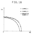
- FIG. 18 shows graphs with respect to current/voltage characteristics of the specimens obtained in Examples 1 and 2 of the present invention and Comparative Example 2 which will be later described.
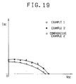
- FIG. 19 shows graphs with respect to further current/voltage characteristics of the specimens obtained in Examples 1 and 2 of the present invention and Comparative Example 2 which will be later described.
- FIG. 1 is a schematic cross section view illustrating the constitution of a pin junction solar cell as an example of the pin junction photovoltaic element of the present invention.
- the pin junction solar cell shown in FIG. l comprises a lower electrode 102, an n-type semiconductor layer 103, an i-type semiconductor layer 104, and a transparent electrode 106 being laminated in this order on a substrate 101.
- Reference numeral 106 stands for a collecting electrode disposed on the transparent electrode 106.
- This pin junction solar cell is of the type that light is impinged from the side of the p-type semiconductor layer 105.
- Each of the lower electrode 102 and the transparent electrode 106 serves as a means to output a photocurrent from the pin junction structure.
- the lower electrode 102 is connected to the n-type semiconductor layer 103 through an ohmic contact, and likewise, the transparent electrode 106 is contacted to the p-type semiconductor layer 105 through an ohmic contact.
- the substrate 101 may be electroconductive or electrically insulating, and it may be transparent or opaque.
- the electroconductive substrate can include, for example, metals such as Al, Fe, Cu, Ni, and Ag and alloys of these metals such as stainless steel.
- the substrate 101 comprises an electroconductive member selected from the group consisting the above metals and alloys
- the substrate may serve also as the lower electrode 102.
- the substrate may also serve as a current-outputting electrode (not shown in the figure).
- the electrically insulating substrate can include, for example, films or sheets of inorganic materials such as no-alkali glass, SiO2, Si3N4, Al2O3 and the like or synthetic resins such as polyimide, polyamide, polyester, polyethylene, polyethylene terephthalate, cellulose acetate, polypropylene, polyvinyl chloride, polystylene, epoxy resin and the like.
- inorganic materials such as no-alkali glass, SiO2, Si3N4, Al2O3 and the like or synthetic resins such as polyimide, polyamide, polyester, polyethylene, polyethylene terephthalate, cellulose acetate, polypropylene, polyvinyl chloride, polystylene, epoxy resin and the like.
- the electrocondutive substrate may comprise a member made of such metal or alloy as above mentioned which has a coat comprising any of the foregoing synthetic resins on the rear face thereof.
- the substrate 101 comprises such electrically insulating film or sheet as above mentioned, it is desired to form an electroconductive thin film of an electroconductive material such as a metal e.g. Al, Ag, Pt, Au, Ni, Ti, Mo, W, Fe, V, Cr or Cu, an alloy e.g. stainless steel, brass, or nichrome, or a transparent and conductive oxide (TCO) material e.g. SnO2, In2O3, or ITO (In2O3 + SnO2) on the surface of the electrically insulating substrate on which a deposited film (the lower electrode 102 or a semiconductor layer) is to be disposed by a metal plating process, a vacuum deposition process process or a sputtering process.
- the electroconductive film formed on the surface of the electrically insulating may function as the foregoing current outputting electrode.
- the substrate 101 even if it is composed of an electroconductive material, may be provided with a metallic layer comprising a metal different from the constituent metal of the substrate on the surface thereof on which a deposited film is to be formed in order to improve the reflection coefficient of long wavelength at the surface of the substrate and also in order to prevent occurrence of mutual diffusion of the constituent materials between the substrate 101 and the deposited film formed on the surface thereof.
- the substrate is constituted by a relatively transparent and conductive material, and a thin film of a transparent and conductive oxide or a metal having a thickness capable of allowing smooth light transmission therethrough is formed on the surface thereof.
- the pin junction solar cell of the type in which light is impinged from the side of the substrate will be later detailed.
- the surface of the substrate prefferably be flat surface or uneven wherein the surface is provided with minute irregularities.
- the irregularity may be of spherical, conical, or pyramid shape in which the maximum height is preferably 500 ⁇ to 5000 ⁇ .
- the pin junction solar cell of the present invention appropriate electrodes are used in accordance with the configuration of the pin junction solar cell to be obtained.
- the lower electrode transparent electrode (upper electrode) and collecting electrode.
- the upper electrode denotes the one to be placed on the side through which light is impinged
- the lower electrode denotes the one to be placed opposite to the upper electrode through the semiconductor layers being arranged between the two electrodes.
- the lower electrode 102 is disposed between the substrate 101 and the n-type semiconductor layer 103 as above described.
- the substrate can function also as the lower electrode 102.
- the lower electrode 102 may be disposed as a lower resistance electrode serving to output a current or in order to heighten the reflectivity of the incident light at the surface of the substrate so as to make it utilized more efficiently.
- the substrate 101 comprises an electrically insulating member, it is essential to dispose the lower electrode 102 serving to output a current, and the lower electrode is placed between the electrically insulating substrate 101 and the corresponding semiconductor layer.
- the lower electrode 102 may comprised of a thin film of a member selected from the group consisting of Ag, Au, Pt, Ni, Cr, Cu, Al, Ti, Zn, Mo, W and alloys of these metals.
- the thin film may be properly formed by way of the known vacuum deposition technique, electron-beam heating deposition technique or sputtering technique.
- the metallic thin film thus formed is not a resistive component for the pin junction solar cell.
- the metallic thin film consisting the lower electrode 102 should be of a sheet resistance preferably of 50 ⁇ or less, more preferably of 10 ⁇ or less.
- a diffusion preventive layer composed of an electroconductive material such as zinc oxide between the lower electrode 102 and the n-type semiconductor layer 103. (This is not shown in the figure).
- diffusion preventive layer is employed in this way, there are provided advantages that it prevents the metal elements constituting the lower electrode 102 from diffusing into the n-type semiconductor layer; it serves to cause multiple interference effects with the thin film and confine the light impinged within the semiconductor layer; and being provided with a certain resistant value, it prevents occurrence of short circuit, which would otherwise occur between the lower electrode 102 and the transparent electrode 106 through the semiconductor layers arranged between them due to pinholes and the like.
- the transparent electrode 106 is desired to have a light transmittance of more than 85% so that it serves to make the semiconductor layer efficiently absorb sunlight or fluorescent light. In addition to this, it is desired to have a sheet resistance of 100 ⁇ or less from the viewpoint of preventing the internal resistance of the pin junction solar cell from becoming great thereby impairing the performance.
- the transparent electrode 106 is desired to comprise a thin film of a metal oxide selected from the group consisting of SnO2, In2O3, ZnO, CdO, Cd2SnO4, and ITO (In2O3 + SnO2) or a semitransparent thin film of a metal selected from the group consisting of Au, Al and Cu.
- a metal oxide selected from the group consisting of SnO2, In2O3, ZnO, CdO, Cd2SnO4, and ITO (In2O3 + SnO2)
- a semitransparent thin film of a metal selected from the group consisting of Au, Al and Cu.
- the transparent electrode 106 is disposed on the p-type semiconductor layer 105. Therefore, it is necessary to constitute the transparent electrode 106 with a thin film member selected from the foregoing which is good in adhesion at least with the p-type semiconductor layer 105.
- the transparent electrode 106 comprising such thin film may be properly formed by way of the known resistance heating deposition technique, electron beam heating deposition technique, sputtering technique or spraying technique.
- the collecting electrode 107 is disposed on the transparent electrode 106 for the purpose of reducing the surface resistance of the transparent electrode.
- the collecting electrode 107 is desired to comprise a thin film of a member selected from the group consisting of Ag, Cr, Ni, Al, Au, Ti, Pt, Cu, Mo and alloys of these metals. It is possible for the collecting electrode to be constituted by a member comprising a plurality of such metallic thin films being laminated.
- the shape and the area of the collecting electrode 107 should be properly designed so that a sufficient quantity of light can be received by the semiconductor layer. Specifically as for the shape, it is desired to be such that it extends uniformly all over the light receiving face of the pin junction solar cell. As for the area, it is desired to be made such that it covers 15% or less of said light receiving face in a preferred embodiment or 10% or less in a more preferred embodiment.
- the member constituting the collecting electrode 107 is of a sheet resistance preferably of 50 ⁇ or less or more preferably of 10 ⁇ or less.
- the i-type semiconductor layer 104 is constituted by a a material capable of being adjusted for the band gap.
- Such material can include silicon-containing amorphous materials such as a-Si, a-SiGe, a-SiSn, a-SiPb, etc., microcrystal Si, polycrystal Si, compounds containing an element belonging to the group II and an element belonging to the group VI of the periodic table (hereinafter referred to as "group II-VI compound”) such as CdS, CdTe, etc., and compounds containing an element belonging to the group III and an element belonging to the group V of the periodic table (hereinafter referred to as "group III-V compound”) such as GaAs, InSb, etc.
- group II-VI compound compounds containing an element belonging to the group II and an element belonging to the group VI of the periodic table
- group III-V compound compounds containing an element belonging to the group III and an element belonging to the group V of the periodic table
- the thickness of the i-type semiconductor layer largely differs depending upon the kind of a material by which the layer is constituted. However, for instance, when it is constituted by a-Si, the thickness is desired to be 500 to 8000 ⁇ . Likewise, when it is constituted by other silicon-containing amorphous material such as a-SiGe, the thickness is desired to be 1000 to 5000 ⁇ .
- the band gap in the i-type semiconductor layer l04 is made such that it grades depending upon given positions in the thickness direction and becomes minimum at a given point in the thickness direction (this point will be hereinafter simply called "minimum point”). Particularly, the band gap becomes gradually widened as the distance from the minimum point to the interface between the i-type semiconductor layer 104 and the n-type semiconductor layer 103 becomes shortened. And the i-type semiconductor layer 104 is desired to be smoothly joined with the n-type semiconductor layer 103 such that the band gap is not discontinued at the composition face between the two layers.
- the band gap extending from the minimum point towards the n-type semiconductor layer is made such that its gradient is relatively gentle in the region situated on the side of the minimum point and is relatively steep in the region situated on the side of the n-type semiconductor layer l03.
- the band gap becomes gradually widened as the distance from the minimum point to the interface between the i-type semiconductor layer 104 and the p-type semiconductor layer 105 becomes shortened.
- the i-type semiconductor layer 104 is desired to be smoothly joined with the p-type semiconductor layer 105 such that the band gap is not discontinued at the composition face between the two layers.
- the optimum position of the minimum point in the i-type semiconductor layer is somewhat different depending upon the kind of a material used and the constitution of the pin junction solar cell, but in general, it is desired to be designed such that it is situated in the region near the p-type semiconductor layer in terms of the thickness direction of the i-type semiconductor layer 104.
- the minimum point is designed to be situated in the region between the interface with the p-type semiconductor layer 105 and the position corresponding to one third of the entire thickness of the i-type semiconductor layer 104 which is distant from said interface in the thickness direction of the i-type semiconductor layer l04.
- the minimum point is designed to be situated in the region between the interface with the p-type semiconductor layer 105 and the position corresponding to one fourth of the entire thickness of the i-type semiconductor layer l04 which is distant from said interface in the thickness direction of the i-type semiconductor layer 104.
- FIG. 2 is a schematic diagram illustrating the profile of an energy band of the semiconductor layer of a pin junction solar cell as an example of the pin junction photovoltaic element according to the present invention.
- CB denotes an edge of conduction band
- VB denotes an edge of valence electron band
- the band gap is made minimum (that is, minimum point) at the position (position B) which is situated near the p-type semiconductor layer in the region of the i-type semiconductor layer between the center of the i-type semiconductor layer and the interface A with the p-type semiconductor layer.
- the characteristics of the i-type semiconductor layer containing the region I AB , a region I BC and a region I CD are adjusted so that the band gap is maximum at the interface A between the i-type semiconductor layer and the p-type semiconductor layer and at the interface D between the i-type semiconductor layer and the n-type semiconductor layer and in addition, the gradient of the band gap between the minimum point B and the maximum point D on the side of the n-type semiconductor layer is relatively gentle in the region I BC near the minimum point B and relatively steep in the region I CD near the point D.
- the bad gap is linearly graded in the region I BC , the gradient thereof is then changed at the point C, and it is again linearly graded in the region I CD , wherein the gradient of the band gap in the region I BC is smaller than that in the region I CD .
- the region between the minimum point of the band gap and the interface with the n-type semiconductor layer is divided into three regions and the gradient of the band gap is made different in each of these three regions.
- the gradient of the band gap is step-wise widened from the minimum point towards the interface with the n-type semiconductor layer.
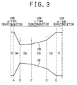
- FIG. 3 is a schematic diagram illustrating the profile of an energy band of the semiconductor layer of a pin junction solar cell as another example of the pin junction photovoltaic element according to the present invention in which the i-type semiconductor region situated between the minimum point B of the band gap and the interface E with the n-type semiconductor layer is divided into three regions I BC , I CD and I DE .
- the gradient of the band gap in the region I CD is wider than that in the region I BC
- the gradient of the band gap in the region I DE is wider than that in the region I CD .
- the thickness of the region I DE is desired to be preferably 510 ⁇ or more, more preferably 550 ⁇ or more.
- pin junction solar cell as a further example of the pin junction photovoltaic element according to the present invention which is of the constitution in which the i-type semiconductor layer region situated between the minimum point of the band gap and the interface with the n-type semiconductor layer is divided into mathematically infinite regions and the gradient of the band gap in each of the regions is changed.
- FIG. 4 is a schematic diagram illustrating the profile of an energy band of the semiconductor layer of a pin junction solar cell as a further example of the pin junction photovoltaic element according to the present invention in which the band gap is gradually graded from the minimum point B towards the interface D with the n-type semiconductor layer without being bent back in the course of grading.
- FIG. 5 is a schematic diagram of illustrating the profile of an energy band of the semiconductor layer of a pin junction solar cell having an intermediate layer as a still further example of the pin junction photovoltaic element according to the present invention.
- the band gap becomes discontinuous at the interface between the i-type semiconductor layer 104 and the n-type semiconductor layer 103 or at the interface the i-type semiconductor layer 104 and the p-type semiconductor layer 104 depending upon the kind of a constituent material used for the formation of each of said semiconductor layers.
- an appropriate layer capable of permitting the band gap to continuously transit therein that is, an intermediate layer
- an appropriate layer capable of permitting the band gap to continuously transit therein that is, an intermediate layer
- each of the two hatched regions B AE and B FD corresponds to the intermediate layer.
- the intermediate layer is disposed at the interface portion between the i-type semiconductor layer 104 and the n-type semiconductor layer 103 in the way as above mentioned, one would think that this cannot be distinguished from the region I DE of the i-type semiconductor layer shown in FIG. 3.
- the intermediate layer B FD is disposed with a thickness of 500 ⁇ or less from the interface with the n-type semiconductor layer l03.
- the gradient of the band gap of the region I DE of the i-type semiconductor layer situated on the side of the n-type semiconductor layer is continuously extended into the inside of the i-type semiconductor layer in the present invention.
- the gradient of the band gap of the region I DE on the side of the n-type semiconductor layer is situated at the portion in the i-type semiconductor layer where the internal electric field is relatively weak and because of this, said gradient contributes to promoting the transportation of a minority carrier to thereby improve the fill factor (F.F.).
- the value of the gradient of the band gap for each of the regions of the i-type semiconductor layer differs depending upon the kind of a material used and also depending upon the entire thickness of the i-type semiconductor layer.
- the gradient of the band gap of, for example, the region I BC of the i-type semiconductor layer on the side near the minimum point of the band gap of the i-type semiconductor layer is desired to be preferably 0.1 to 0.5 eV/ ⁇ m, more preferably 0.2 to 2 eV/ ⁇ m
- the gradient of the band gap of, for example, the region I CD , I CF or I DE of the i-type semiconductor layer on the side near the n-type layer is desired to be preferably 0.5 to 60 eV/ ⁇ m, more preferably 1.0 to 12 eV/ ⁇ m.
- the method of grading the band gap of the i-type semiconductor layer is different depending upon the kind of a material of which the i-type semiconductor layer is formed.
- the band gap can be graded by changing the elemental composition ratio. For example, it is known that in the case where the composition ratio of Si/Ge as for a-SiGe which is suitable for a solar cell, its band gap can be substantially linearly changed depending upon a change in the elemental composition ratio of Si/Ge.
- the bad gap thereof can be properly graded by continuously changing the elemental composition ratio thereof in the thickness direction in accordance with the above known method.
- its band gap can be properly graded by changing the hydrogen content or the size of crystal grains as desired.
- the n-type semiconductor layer 103 may be constituted by any of the foregoing materials usable for the formation of the i-type semiconductor layer 104.
- the n-type semiconductor layer 103 may be constituted also by other appropriate material having a band gap wider than that of a-Si such as a-SiC, a-SiN, a-SiO or the like.
- these materials are made to be of n-type by doping them with an appropriate dopant such as P, As, Sb, N, etc. upon forming the n-type semiconductor layer.
- the p-type semiconductor layer 105 may be constituted by any of the materials usable for the formation of the n-type semiconductor layer 103.
- any of those materials is made to be of p-type by doping it with an appropriate dopant such as B, Al, Ga, In, etc. upon forming the p-type semiconductor layer.
- n-type semiconductor layer 103 and the p-type semiconductor layer 105 is desired to be such that is low in resistance, small in activation energy and little in defect.
- the semiconductor layer positioned on the side through which light is impinged is designed to have a wider band gap and to be thin in thickness so that light transmission is heightened.
- each of the n-type semiconductor layer 103 and the p-type semiconductor layer 105 the optimum value thereof largely differs depending upon the kind of a material to be used for the formation of each of them.
- the thickness of each of them is desired to be in the range of from 30 to 500 ⁇ .
- the foregoing pin junction solar cell having the configuration shown in FIG. 1 is of the type in which light is impinged from the side opposite the substrate 101. This configuration can be changed to such that light is impinged from the side of the substrate.
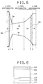
- FIG. 6 is a schematic cross section view illustrating the configuration of a pin junction solar cell of the type in which light is impinged from the side of the substrate.
- the pin junction solar cell shown in FIG. 6 comprises a transparent electrode 116, an n-type semiconductor layer ll3, an i-type semiconductor layer 114, an n-type semiconductor layer 115, and a lower electrode 112 being laminated in this order on a light transmissive substrate 111.
- Each of the transparent electrode 116, the n-type semiconductor layer 113, the i-type semiconductor layer 114, the n-type semiconductor layer 115, and the lower electrode 112 is formed in the same manner as above described of the pin junction solar cell shown in FIG. 1.
- the substrate 111 in the pin junction solar cell shown in FIG. 6 is desired to have been applied with an electroconductive oxide thin film or a metallic thin film of a thickness capable of permitting light to transmit therethrough to the surface thereof.
- the transparent electrode 116 is positioned between the substrate lll and the n-type semiconductor layer 113, the transparent electrode is desired to be constituted by a material having a good adhesion not only with the substrate 111 but also with the n-type semiconductor layer 113.
- the pin junction solar cell of the present invention may be a pin junction multicells-stacked solar cell comprising a plurality of pin junction photovoltaic elements respectively, for example, of the same constitution as the pin junction element of the pin junction solar cell shown in FIG. 1 being stacked.
- Such solar cell module is prepared in a manner that a plurality of such solar cell units are electrically connected either in series or in parallel to thereby integrate them, whereby obtaining an integrated body, a layer capable of protecting the surface thereof is mounted to the integrated body, and outputting terminals are provided to the resultant.
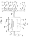
- This film-forming apparatus serves to form a deposited film on a substrate by means of a high frequency plasma CVD process, and it is of the known constitution.
- reference numeral 201 stands for a deposition chamber provided with a gas feed pipe 208 serving to introduce a film-forming raw material gas into said deposition chamber and an exhaust pipe 206 connected through an exhaust valve (not shown) to a vacuum pump 207.
- a substrate holder 204 and a high frequency electrode 204 to be opposite to said substrate holder.
- the substrate holder 204 is constituted by a conductive material, and it is electrically grounded.
- Reference numeral 101 stand for a substrate placed on the surface of the substrate holder 204.
- Reference numeral 205 stands for an electric heater installed in the substrate holder 204. The electric heater 205 serves to heat the substrate 101.
- the high frequency electrode 203 is electrically connected through a matching box (not shown) to a high frequency power source 202 which is electrically grounded.
- the other end of the gas feed pipe 208 is connected to raw material gas reservoirs (not shown) through branch pipes 209 provided with excit valves 210, mass flow controllers 212 and main valves 211 for the reservoirs.
- An appropriate raw material gas is reserved in each of the reservoirs.
- the raw material gas from each of the reservoirs is introduced into the deposition chamber 201 through the main valve 211, the mass flow controller 212, the excit valve 210 and the gas feed pipe 208 while its flow rate being controlled.
- the flow rate of each of the film-forming raw material gases to be thus introduced into the deposition chamber 20l upon film formation can be properly changed as desired by controlling the corresponding mass flow controller.
- Each of the mass flow controllers 211 is designed such that it can be properly controlled by a microcomputer (not shown). Thus, a desired flow rate pattern can be attained by programing said microcomputer.
- Film formation in this film-forming apparatus is performed, for example, in such a manner that the inside of the deposition chamber 201 is evacuated to a predetermined vacuum degree by the action of the vacuum pump 207, one or more kinds of film-forming raw material gases are introduced thereinto through the gas feed pipe 208 while controlling their flow rates as desired, simultaneously the high frequency power source 202 is switched on to apply a predetermined high frequency power to the high frequency electrode 203 to thereby cause glow discharge, whereby forming a deposited film on the surface of the substrate 101 being maintained at a desired temperature.
- Film formation using the film-forming apparatus shown in FIG. 7 in this example was performed as follows.
- a SUS 304 stainless steel plate of 5 cm x 5 cm in size having a mirror ground uneven surface of 0.05 ⁇ m in Rmax.
- this substrate 101 On the surface of this substrate 101 were successively formed a 1000 ⁇ thick Ag film and a 4000 ⁇ thick ZnO film to be the lower electrode 102 by a conventional high frequency sputtering method. At the time of forming said Ag thin film, the substrate was maintained at about 300 °C in order to make the surface of said Ag film to be uneven (to be textured in other words).
- the substrate having the lower electrode 102 formed thereon was placed on the surface of the substrate holder 204 of the film-forming apparatus shown in FIG. 7. Then, the inside of the deposition chamber 201 was evacuated by actuating the vacuum pump 207 to bring it to a vacuum degree of about 1 x 10 ⁇ 6 Torr. The vacuum degree in this case was observed by an ion gage (not shown).
- the heater 205 was actuated to heat the substrate 101 to about 300 °C. After the temperature of the substrate 101 became constant at this temperature, the main valve 211 and the exit valve 210 were operated to introduce Si2H6 gas into the deposition chamber 201 at a flow rate of 1 sccm while controlling its flow rate by means of the mass flow controller 212.
- H2 gas and PH3/H2 gas (diluted to 5%) were introduced into the deposition chamber 201 at respective flow rates of 50 sccm and 1 sccm.
- the gas pressure in the deposition chamber 201 was adjusted to and maintained at 1.2 Torr.
- the high frequency power source 202 was switched on to apply a high frequency power of l.5 W to the high frequency electrode 203, to thereby cause glow discharge in the deposition chamber.
- This film forming procedure was continued for 2 minutes.
- an about 200 ⁇ thick n-type a-Si:H film to be the n-type semiconductor layer 103 on the lower electrode 102.
- the application of the high frequency power and the introduction of the gases were suspended.
- the inside of the deposition chamber 201 was evacuated to a vacuum degree of about 1 x 10 ⁇ 6 Torr. Then film formation was performed in the same manner as in the case of forming the n-type semiconductor layer 103 under the following conditions. raw material gases used & their flow rates:
- the resultant non-doped a-SiGe:H film was found to have such band gap graded in the thickness direction as shown in FIG. 9.
- the inside of the deposition chamber 201 was evacuated to a vacuum degree of about 1 x 10 ⁇ 6 Torr.
- the p-type semiconductor layer 105 was formed in the same manner as in the case of forming the n-type semiconductor layer 103 under the following conditions.
- the application of the high frequency power and the introduction of the gases were terminated.
- the resultant was cooled, and it was transferred into a conventional vacuum deposition apparatus, wherein on the previously formed p-type semiconductor layer was formed a 700 ⁇ thick ITO film to be the transparent electrode 106.
- the sample thus obtained was cut into a plurality of specimens respectively of 1 cm x 1 cm in size.
- On each of the specimens was formed an aluminum thin film to be the collecting electrode 107 by a conventional electron beam heating deposition process.
- a plurality of solar cell samples there were obtained a plurality of solar cell samples.
- the characteristics to sunlight were examined by subjecting it to irradiation with AM-l.5 light of 100 mW/cm2 in intensity, which has spectra approximate to sunlight spectra in terms of AM value, using a solar simulator with a xenon lamp.
- AM-1.5 light of 100 mW/cm2 in intensity was irradiated through a filter (which does not permit light of less than 600 nm in wavelength to transmit therethrough) to each of the solar cell samples, to thereby examine its characteristics to long wavelength light with respect to the same evaluation items as in the above.
- the above procedures of forming the i-type semiconductor layer 104 were repeated to form a non-doped a-SiGe:H film on a glass plate.
- the profile of the optical band gap (Eg opt) was observed based on the wavelength properties in the relation between a given wavelength and light extinction coefficient which were obtained in accordance with a conventional optical band gap evaluating method, for example, disclosed in The Basis of Amorphous Semiconductors, edited by M. Kikuchi et al, pp. 90-92, published by Kabushiki Kaisha Ohm Sha, May l0, l983).
- the Ge content was observed by a commercially available X-ray microanalyzer (XMA).
- XMA X-ray microanalyzer
- Table 1 the results shown in Table 1 were graphically illustrated in FIG. 9. From what shown in Table 1 and FIG. 9, it is understood that the gradient of the optical band gap in the region of the i-type semiconductor layer 104 situated on the side of the n-type semiconductor layer 103, that is, in the region between C and D in FIG. 9, is 2.7 eV/ ⁇ m; the gradient of the optical band gap between the minimum point B of the optical band gap of the i-type semiconductor layer and said point C is 0.67 eV/ ⁇ m; and the gradient of the former optical band gap is greater than that of the latter optical band gap.
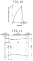
- the i-type layer comprising a-SiGe:H film was formed by repeating the same procedures of forming the i-type semiconductor layer 104 in Example 1, except that GeH4 gas was introduced into the deposition chamber 201 following the flow rate pattern shown in FIG. 10. Particularly in this respect, the mass flow controller for the GeH4 gas was controlled so that the flow rate of GeH4 gas followed the convex curve from the interface (D point in FIG. l0) with the n-type semiconductor layer 103 to the minimum point (B point in FIG. l0) of the band gap of an i-type semiconductor layer to be formed.
- the sample thus obtained was cut into a plurality of specimens respectively of 1 cm x 1 cm in size.
- On each of the specimens was formed an aluminum thin film to be the collecting electrode 107 by a conventional electron beam heating deposition process.
- a plurality of solar cell samples there were obtained a plurality of solar cell samples.
- AM-1.5 light of 100 mW/cm2 in intensity was irradiated through a filter (which does not permit light of less than 600 nm in wavelength to transmit therethrough) to each of the solar cell samples, to thereby examine its characteristics to long wavelength light with respect to the same evaluation items as in the above.
- This solar cell is one that does not have any gradient in the band gap of the i-type semiconductor layer.
- FIG. 16 shows the profile of an energy band of this solar cell.
- an intermediate layer B AE a graded intermediate layer B EB and a graded intermediate layer in the i-type semiconductor layer in order to reduce a discontinuation in the band gap at the interface between the p-type semiconductor layer and the i-type semiconductor layer and at the interface between the n-type semiconductor layer and the i-type semiconductor layer and in order to reduce interface states.
- the optical band gap Eg opt of the region I BF in the i-type semiconductor layer is l.45 eV.
- the comparative pin junction a-SiGe solar cell of the known constitution was prepared by repeating the procedures of Example 1, except for the step of forming the i-type semiconductor layer.
- the i-type layer of the comparative pin junction solar cell was formed by repeating the same procedures of forming the i-type semiconductor layer 104 in Example 1, except that GeH4 gas was introduced into the deposition chamber 201 while controlling the flow rate thereof from 0 sccm to 0.6 sccm, to thereby form a 200 ⁇ thick i-type film as the i-type semiconductor layer containing the foregoing intermediate layer and the foregoing two graded intermediate layers with the band gap constitution shown in FIG. 16.
- the sample thus obtained was cut into a plurality of specimens respectively of 1 cm x 1 cm in size.
- On each of the specimens was formed an aluminum thin film to be the collecting electrode 107 by a conventional electron beam heating deposition process.
- a plurality of solar cell samples there were obtained a plurality of solar cell samples.
- AM-1.5 light of l00 mW/cm2 in intensity was irradiated through a filter (which does not permit light of less than 600 nm in wavelength to transmit therethrough) to each of the solar cell samples, to thereby examine its characteristics to long wavelength light with respect to the same evaluation items as in the above.
- This solar cell is such that the band gap of a region I BC comprising an i-type semiconductor adjacent to the n-type semiconductor layer is widened on the side of the n-type semiconductor layer, the band gap is minimum at the boundary portion between a region I EB and a region I BC of the i-type semiconductor layer, and an intermediate layer B AE is present between a p-type semiconductor region P and the region I EB .
- This comparative solar cell was prepared by repeating the procedures of Example 1, except for the step of forming the i-type semiconductor layer.
- the i-type layer of the comparative pin junction solar cell was formed by repeating the same procedures of forming the i-type semiconductor layer 104 in Example 1, except that GeH4 gas was introduced into the deposition chamber 201 while controllin the flow rate thereof from 0 sccm to 0.6 sccm, to thereby form a 200 ⁇ thick i-type semiconductor layer having the band gap constitution shown in FIG. 17.
- the sample thus obtained was cut into a plurality of specimens respectively of 1 cm x 1 cm in size.
- On each of the specimens was formed an aluminum thin film to be the collecting electrode 107 by a conventional electron beam heating deposition process.
- a plurality of solar cell samples there were obtained a plurality of solar cell samples.
- AM-1.5 light of 100 mW/cm2 in intensity was irradiated through a filter (which does not permit light of less than 600 nm in wavelength to transmit therethrough) to each of the solar cell samples, to thereby examine its characteristics to long wavelength light with respect to the same evaluation items as in the above.
- Film formation using the film-forming apparatus shown in FIG. 7 in this example was performed as follows.
- the substrate 111 there was provided a no-alkali glass (commercially available under the trade name : No.7059 glass, produced by Corning Glass Works Company) of 5 cm x 5 cm in size.
- this substrate lll On the surface of this substrate lll were successively formed a 1800 ⁇ thick ITO film and a 200 ⁇ thick SnO2 film to be the transparent electrode 1116 by a conventional vacuum deposition high method, followed by subjecting to pattering into a lattice pattern.
- the substrate having the transparent electrode 116 formed thereon was placed on the surface of the substrate holder 204 of the film-forming apparatus shown in FIG. 7. Then, the inside of the deposition chamber 201 was evacuated by actuating the vacuum pump 207 to bring it to a vacuum degree of about 1 x 10 ⁇ 6 Torr. The vacuum degree in this case was observed by an ion gage (not shown).
- the heater 205 was actuated to heat the substrate lll to about 260 °C. After the temperature of the substrate lll became constant at this temperature, the main valve 2ll and the exit valve 210 were operated to introduce Si2H6 gas into the deposition chamber 201 at a flow rate of 1 sccm while controlling its flow rate by means of the mass flow controller 212.
- H2 gas and PH3/H2 gas (diluted to 5%) and CH4 gas were introduced into the deposition chamber 201 at respective flow rates of 50 sccm, 1 sccm and 4 sccm.
- the gas pressure in the deposition chamber 20l was adjusted to and maintained at 1.2 Torr.
- the high frequency power source 202 was switched on to apply a high frequency power of l.5 W to the high frequency electrode 203, to thereby cause glow discharge in the deposition chamber.
- This film forming procedure was continued for 2 minutes.
- an about l20 ⁇ thick n-type a-SiC:H film to be the n-type semiconductor layer 113 on the transparent electrode ll6.
- the application of the high frequency power and the introduction of the gases were suspended.
- the inside of the deposition chamber 20l was evacuated to a vacuum degree of about l x l0 ⁇ 6 Torr.
- an intermediate layer comprising a-SiC:H was formed in the region adjacent to the n-type semiconductor layer by introducing CH4 gas at a linearly reducing flow rate starting at 4 sccm and ending at 0 sccm at the time when the period of 3 minutes laps as shown in Table 12 while not introducing the GH4 gas, and during last 3 minute's period, another intermediate layer comprising a-Si:H was formed without introducing the GeH4 gas.
- the resultant i-type semiconductor layer was found to have such band gap structure as shown in FIG. 13.
- the region B FD corresponds to the former intermediate layer and the region B AE corresponds to the latter intermediate layer.
- the inside of the deposition chamber 20l was evacuated to a vacuum degree of about 1 x 10 ⁇ 6 Torr.
- the p-type semiconductor layer 115 was formed in the same manner as in the case of forming the n-type semiconductor layer 113 under the following conditions.
- the application of the high frequency power and the introduction of the gases were terminated.
- the resultant was cooled, and it was transferred into a conventional vacuum deposition apparatus, wherein on the previously formed p-type semiconductor layer were successively formed a 200 ⁇ thick Cr film and a 1800 ⁇ thick Al film to be the lower electrode 112, followed by subjecting to patterning.
- the sample thus obtained was cut into a plurality of specimens respectively of l cm x 1 cm in size. Thus, there were obtained a plurality of solar cell samples.
- AM-l.5 light of 100 mW/cm2 in intensity was irradiated through a filter (which does not permit light of less than 600 nm in wavelength to transmit therethrough) to each of the solar cell samples, to thereby examine its characteristics to long wavelength light with respect to the same evaluation items as in the above.
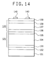
- pin junction tandem type solar cell comprising two pin junction solar cell units being stacked of the configuration shown in FIG. 14.
- the pin junction tandem type solar cell shown in FIG. 14 comprises a lower electrode 132, a first pin junction cell unit l2l (comprising a first n-type semiconductor layer 133, a first i-type semiconductor layer 134 and a first p-type semiconductor layer l35 being laminated), a second pin junction solar cell unit l22 (comprising a second n-type semiconductor layer l36, a second i-type semiconductor layer 137 and a second p-type semiconductor layer 138 being laminated) and a transparent electrode 139 being stacked in this order on a substrate 131.
- Reference numeral 140 stands for a collecting electrode disposed on the transparent electrode 139.
- the first i-type semiconductor layer 134 has a bad gap graded in the thickness direction as well as the i-type semiconductor layer of the pin junction solar cell obtained in Example 1, but the second i-type semiconductor layer l37 does not have such graded band gap.
- This pin junction tandem type solar cell was prepared in the following manner.
- this substrate 131 On the surface of this substrate 131 were successively formed a 1000 ⁇ thick Ag film and a 4000 ⁇ thick ZnO film to be the lower electrode 132 by a conventional high frequency sputtering method.
- the substrate having the lower electrode 132 formed thereon was placed on the surface of the substrate holder 204 of the film-forming apparatus shown in FIG. 7.
- Example 2 by repeating the procedures of Example 1, on the lower electrode 132 were formed the first n-type semiconductor layer l33 and the first i-type semiconductor layer 134. Thereafter, the procedures of forming the p-type semiconductor layer were repeated, except that the substrate temperature was changed to 260 °C, to thereby form the first p-type semiconductor layer 135. Thus, there was formed the first pin junction solar cell unit l2l.
- Example 1 Successively the procedures of Example 1 for forming the n-type semiconductor layer in Example 1 were repeated, except that the substrate temperature was changed to 240 °C, to thereby form the second n-type semiconductor layer 136 of 180 ⁇ in thickness on the previously formed first p-type semiconductor layer 135.
- the application of the high frequency power and the introduction of the gases were suspended.
- the inside of the deposition chamber 201 was evacuated to a vacuum degree of about 1 x 10 ⁇ 6 Torr.
- the formation of the second i-type semiconductor layer 137 was performed in the same manner as in the case of forming the n-type semiconductor layer in Example 1 and under the following conditions. raw material gases used & their flow rates:
- Example 1 Successively the procedures of Example 1 for forming the p-type semiconductor layer were repeated, except that the substrate temperature was changed to 200 °C, to thereby form the second p-type semiconductor layer 138 of 50 ⁇ in thickness on the previously formed second i-type semiconductor layer 137.
- the application of the high frequency power and the introduction of the gases were terminated.
- the resultant was cooled, and it was transferred into a conventional vacuum deposition apparatus, wherein on the previously formed p-type semiconductor layer 138 was formed a 700 ⁇ thick ITO film to be the transparent electrode 139.
- the sample thus obtained was cut into a plurality of specimens respectively of 1 cm x 1 cm in size.
- On each of the specimens was formed an aluminum thin film to be the collecting electrode 140 by a conventional electron beam heating deposition process.
- a plurality of solar cell samples there were obtained a plurality of solar cell samples.
- AM-l.5 light of l00 mW/cm2 in intensity was irradiated through a filter (which does not permit light of less than 600 nm in wavelength to transmit therethrough) to each of the solar cell samples, to thereby examine its characteristics to long wavelength light.
- each of the solar cell samples was found to be excel in the characteristics to long wavelength light. From these results, it was found that any of the solar cell samples exhibits an improved photoelectric conversion efficiency.
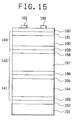
- the pin junction triple cell type solar cell shown in FIG. 15 comprises a lower electrode 152, a first pin junction cell unit 141 (comprising a first n-type semiconductor layer 153, a first i-type semiconductor layer 154 and a first p-type semiconductor layer 155 being laminated), a second pin junction solar cell unit 142 (comprising a second n-type semiconductor layer 156, a second i-type semiconductor layer 157 and a second p-type semiconductor layer 158 being laminated), a third pin junction solar cell unit 143 (comprising a third n-type semiconductor layer 159, a third i-type semiconductor layer 160 and a third p-type semiconductor layer 161 being laminated), and a transparent electrode l62 being stacked in this order on a substrate 151.
- Reference numeral 163 stands for a collecting electrode disposed on the transparent electrode 162.
- the first i-type semiconductor layer 154 has a bad gap graded in the thickness direction as well as the i-type semiconductor layer of the pin junction solar cell obtained in Example 2, but each of the second and third i-type semiconductor layers 157 and 160 does not have such graded band gap.
- This pin junction triple cell type solar cell was prepared in the following manner.
- the substrate 151 there was provided a SUS 304 stainless steel plate.
- this substrate 151 On the surface of this substrate 151 were successively formed a 1000 ⁇ thick Ag film and a 4000 ⁇ thick ZnO film to be the lower electrode 152 by a conventional high frequency sputtering method.
- the substrate having the lower electrode 152 formed thereon was placed on the surface of the substrate holder 204 of the film-forming apparatus shown in FIG. 7.
- Example 2 for forming the i-type semiconductor layer were repeated, except that the substrate temperature was changed to 320 °C, to thereby form the first i-type semiconductor layer 154 comprising a-SiGe:H.
- Example 1 for forming the p-type semiconductor layer were repeated, except that the substrate temperature was changed to 300 °C, to thereby form the first p-type semiconductor layer 155.
- the first pin junction solar cell unit 141 with a pin junction having a graded band gap similar to that in Example 2 which is shown in FIG. 11.
- Example 1 for forming the n-type semiconductor layer were repeated, except that the substrate temperature was changed to 280 °C, to thereby form the second n-type semiconductor layer 156 comprising a-Si:H.
- Example 4 for forming the second i-type semiconductor layer were repeated, except that the substrate temperature was changed to 280 °C and film formation was performed for 75 minutes, to thereby form the second i-type semiconductor layer 157 comprising a 5000 ⁇ thick a-Si:H film.
- the procedures of Example 1 for forming the p-type semiconductor layer were repeated to thereby form the second p-type semiconductor layer 158.
- the second pin junction solar cell unit 142 with a pin junction not having a graded band gap.
- Example 1 for forming the n-type semiconductor layer were repeated, except that the substrate temperature was changed to 220 °C, to thereby form the third n-type semiconductor layer 159 comprising a-Si:H.
- Example 4 for forming the second i-type semiconductor layer were repeated, except that film formation was performed for 12 minutes, to thereby form the third i-type semiconductor layer 160 comprising a 800 ⁇ thick a-Si:H film.
- the procedures of Example 4 for forming the second p-type semiconductor layer were repeated to thereby form the third p-type semiconductor layer 161.
- the third pin junction solar cell unit 143 with a pin junction not having a graded band gap.
- the application of the high frequency power and the introduction of the gases were terminated.
- the resultant was cooled, and it was transferred into a conventional vacuum deposition apparatus, wherein on the previously formed p-type semiconductor layer 161 was formed a 700 ⁇ thick ITO film to be the transparent electrode 162.
- the sample thus obtained was cut into a plurality of specimens respectively of 1 cm x 1 cm in size.
- On each of the specimens was formed an aluminum thin film to be the collecting electrode 163 by a conventional electron beam heating deposition process.
- a plurality of solar cell samples there were obtained a plurality of solar cell samples.
- AM-1.5 light of 100 mW/cm2 in intensity was irradiated through a filter (which does not permit light of less than 600 nm in wavelength to transmit therethrough) to each of the solar cell samples, to thereby examine its characteristics to long wavelength light.
- each of the solar cell samples was found to be excel in the characteristics to long wavelength light. From these results, it was found that any of the solar cell samples exhibits an improved photoelectric conversion efficiency.
- a pin junction photovoltaic element having an i-type semiconductor layer formed of a band gap variable semiconductor material between a p-type semiconductor layer having a band gap wider than that of said i-type semiconductor layer and an n-type semiconductor layer having a band gap wider than that of said i-type semiconductor layer, characterized in that said i-type semiconductor layer contains a first region which is positioned on the side of said p-type semiconductor layer and has a graded band gap, a second region which is adjacent to said first region and has a graded band gap, and a third region which is positioned on the side of said n-type semiconductor layer and has a graded band gap; said i-type semiconductor layer has a minimum band gap at the boundary between said first region and said second region; the thickness of said first region is less than one second: of the thickness of said i-type semiconductor layer; and the gradient of the graded band gap of said third region is larger than that of the band gap of said second region.
Landscapes
- Photovoltaic Devices (AREA)
Applications Claiming Priority (2)
| Application Number | Priority Date | Filing Date | Title |
|---|---|---|---|
| JP2315924A JP2719230B2 (ja) | 1990-11-22 | 1990-11-22 | 光起電力素子 |
| JP315924/90 | 1990-11-22 |
Publications (3)
| Publication Number | Publication Date |
|---|---|
| EP0487114A2 true EP0487114A2 (de) | 1992-05-27 |
| EP0487114A3 EP0487114A3 (en) | 1993-09-22 |
| EP0487114B1 EP0487114B1 (de) | 1996-05-29 |
Family
ID=18071245
Family Applications (1)
| Application Number | Title | Priority Date | Filing Date |
|---|---|---|---|
| EP91120051A Expired - Lifetime EP0487114B1 (de) | 1990-11-22 | 1991-11-22 | Photovoltaisches Bauelement mit Pin-Übergang, mit einer i-Typ Halbleiter-Schicht bestehend aus einer Mehrzahl von Gebieten mit verschiedenen, gradierten Energiebandabständen |
Country Status (4)
| Country | Link |
|---|---|
| US (1) | US5252142A (de) |
| EP (1) | EP0487114B1 (de) |
| JP (1) | JP2719230B2 (de) |
| DE (1) | DE69119870T2 (de) |
Cited By (8)
| Publication number | Priority date | Publication date | Assignee | Title |
|---|---|---|---|---|
| EP0631329A1 (de) * | 1993-06-25 | 1994-12-28 | Showa Shell Sekiyu K.K. | Herstellungsverfahren einer aus amorphen Silizium bestehenden Solarzelle |
| EP1918966A1 (de) * | 2006-11-02 | 2008-05-07 | Dow Corning Corporation | Verfahren zur Herstellung einer Schicht mit gradiertem Bandabstand durch Abscheidung eines amorphen Stoffes aus einem Plasma |
| US7998785B2 (en) | 2006-11-02 | 2011-08-16 | Dow Corning Corporation | Film deposition of amorphous films with a graded bandgap by electron cyclotron resonance |
| WO2011129708A1 (en) * | 2010-04-16 | 2011-10-20 | Institutt For Energiteknikk | Thin film solar cell electrode with graphene electrode layer |
| US8349412B2 (en) | 2006-11-02 | 2013-01-08 | Ecole Polytechnique | Deposition of amorphous silicon films by electron cyclotron resonance |
| US8383210B2 (en) | 2006-11-02 | 2013-02-26 | Dow Corning Europe S.A. | Method of forming a film by deposition from a plasma |
| US8635972B2 (en) | 2006-11-02 | 2014-01-28 | Ecole Polytechnique | Device for forming a film by deposition from a plasma |
| US8859929B2 (en) | 2006-11-02 | 2014-10-14 | Dow Corning Corporation | Method and apparatus for forming a film by deposition from a plasma |
Families Citing this family (82)
| Publication number | Priority date | Publication date | Assignee | Title |
|---|---|---|---|---|
| JP2951146B2 (ja) * | 1992-04-15 | 1999-09-20 | キヤノン株式会社 | 光起電力デバイス |
| JP2761156B2 (ja) * | 1992-06-30 | 1998-06-04 | キヤノン株式会社 | 光起電力素子及びその製造方法、並びにそれを用いた発電装置 |
| US5668395A (en) * | 1994-11-22 | 1997-09-16 | Northwestern University | Composition for InSB and GaAs thin film on silicon substrate for use in photodetectors |
| US5594237A (en) * | 1995-02-24 | 1997-01-14 | The Whitaker Corporation | PIN detector having improved linear response |
| US7907319B2 (en) * | 1995-11-06 | 2011-03-15 | Qualcomm Mems Technologies, Inc. | Method and device for modulating light with optical compensation |
| US5818096A (en) * | 1996-04-05 | 1998-10-06 | Nippon Telegraph And Telephone Corp. | Pin photodiode with improved frequency response and saturation output |
| US6147391A (en) * | 1996-05-07 | 2000-11-14 | The Regents Of The University Of California | Semiconductor hetero-interface photodetector |
| US6074892A (en) | 1996-05-07 | 2000-06-13 | Ciena Corporation | Semiconductor hetero-interface photodetector |
| AU729609B2 (en) * | 1996-08-28 | 2001-02-08 | Canon Kabushiki Kaisha | Photovoltaic device |
| US8928967B2 (en) | 1998-04-08 | 2015-01-06 | Qualcomm Mems Technologies, Inc. | Method and device for modulating light |
| WO1999052006A2 (en) | 1998-04-08 | 1999-10-14 | Etalon, Inc. | Interferometric modulation of radiation |
| WO2003007049A1 (en) | 1999-10-05 | 2003-01-23 | Iridigm Display Corporation | Photonic mems and structures |
| US6548751B2 (en) * | 2000-12-12 | 2003-04-15 | Solarflex Technologies, Inc. | Thin film flexible solar cell |
| US8084265B2 (en) * | 2001-05-05 | 2011-12-27 | Alliance for Sustianable Energy, LLC | Method and Pd/V2 O5 device for H2 detection |
| US7122736B2 (en) * | 2001-08-16 | 2006-10-17 | Midwest Research Institute | Method and apparatus for fabricating a thin-film solar cell utilizing a hot wire chemical vapor deposition technique |
| JP2004134748A (ja) | 2002-07-26 | 2004-04-30 | Canon Inc | 光電変換素子の測定方法および装置、光電変換素子の製造方法及び製造装置 |
| TWI284443B (en) * | 2003-01-07 | 2007-07-21 | Au Optronics Corp | Automatic control system and method of laser energy |
| US6815790B2 (en) * | 2003-01-10 | 2004-11-09 | Rapiscan, Inc. | Position sensing detector for the detection of light within two dimensions |
| JP4171428B2 (ja) * | 2003-03-20 | 2008-10-22 | 三洋電機株式会社 | 光起電力装置 |
| US7256470B2 (en) * | 2005-03-16 | 2007-08-14 | Udt Sensors, Inc. | Photodiode with controlled current leakage |
| US8686529B2 (en) * | 2010-01-19 | 2014-04-01 | Osi Optoelectronics, Inc. | Wavelength sensitive sensor photodiodes |
| US7709921B2 (en) | 2008-08-27 | 2010-05-04 | Udt Sensors, Inc. | Photodiode and photodiode array with improved performance characteristics |
| US7655999B2 (en) | 2006-09-15 | 2010-02-02 | Udt Sensors, Inc. | High density photodiodes |
| US7656001B2 (en) * | 2006-11-01 | 2010-02-02 | Udt Sensors, Inc. | Front-side illuminated, back-side contact double-sided PN-junction photodiode arrays |
| US8519503B2 (en) * | 2006-06-05 | 2013-08-27 | Osi Optoelectronics, Inc. | High speed backside illuminated, front side contact photodiode array |
| US7576369B2 (en) * | 2005-10-25 | 2009-08-18 | Udt Sensors, Inc. | Deep diffused thin photodiodes |
| US7880258B2 (en) * | 2003-05-05 | 2011-02-01 | Udt Sensors, Inc. | Thin wafer detectors with improved radiation damage and crosstalk characteristics |
| US7242069B2 (en) * | 2003-05-05 | 2007-07-10 | Udt Sensors, Inc. | Thin wafer detectors with improved radiation damage and crosstalk characteristics |
| US7279731B1 (en) | 2006-05-15 | 2007-10-09 | Udt Sensors, Inc. | Edge illuminated photodiodes |
| US8035183B2 (en) * | 2003-05-05 | 2011-10-11 | Udt Sensors, Inc. | Photodiodes with PN junction on both front and back sides |
| US8164151B2 (en) * | 2007-05-07 | 2012-04-24 | Osi Optoelectronics, Inc. | Thin active layer fishbone photodiode and method of manufacturing the same |
| US7057254B2 (en) * | 2003-05-05 | 2006-06-06 | Udt Sensors, Inc. | Front illuminated back side contact thin wafer detectors |
| US8120023B2 (en) * | 2006-06-05 | 2012-02-21 | Udt Sensors, Inc. | Low crosstalk, front-side illuminated, back-side contact photodiode array |
| DE102005013537A1 (de) * | 2004-03-24 | 2005-10-20 | Sharp Kk | Fotoelektrischer Wandler und Herstellverfahren für einen solchen |
| US20070023081A1 (en) * | 2005-07-28 | 2007-02-01 | General Electric Company | Compositionally-graded photovoltaic device and fabrication method, and related articles |
| US7906723B2 (en) * | 2008-04-30 | 2011-03-15 | General Electric Company | Compositionally-graded and structurally-graded photovoltaic devices and methods of fabricating such devices |
| US7916980B2 (en) | 2006-01-13 | 2011-03-29 | Qualcomm Mems Technologies, Inc. | Interconnect structure for MEMS device |
| US7655542B2 (en) * | 2006-06-23 | 2010-02-02 | Applied Materials, Inc. | Methods and apparatus for depositing a microcrystalline silicon film for photovoltaic device |
| US7714300B1 (en) | 2006-06-27 | 2010-05-11 | Kla-Tencor Technologies Corporation | High-speed high-efficiency solid-state electron detector |
| US20080000522A1 (en) * | 2006-06-30 | 2008-01-03 | General Electric Company | Photovoltaic device which includes all-back-contact configuration; and related processes |
| US9178092B2 (en) | 2006-11-01 | 2015-11-03 | Osi Optoelectronics, Inc. | Front-side illuminated, back-side contact double-sided PN-junction photodiode arrays |
| US20080110486A1 (en) | 2006-11-15 | 2008-05-15 | General Electric Company | Amorphous-crystalline tandem nanostructured solar cells |
| US20080135089A1 (en) * | 2006-11-15 | 2008-06-12 | General Electric Company | Graded hybrid amorphous silicon nanowire solar cells |
| CN101569017B (zh) | 2006-12-25 | 2011-11-30 | 夏普株式会社 | 光电转换装置及其制造方法 |
| US7977568B2 (en) | 2007-01-11 | 2011-07-12 | General Electric Company | Multilayered film-nanowire composite, bifacial, and tandem solar cells |
| US20080173350A1 (en) * | 2007-01-18 | 2008-07-24 | Applied Materials, Inc. | Multi-junction solar cells and methods and apparatuses for forming the same |
| US20080223440A1 (en) * | 2007-01-18 | 2008-09-18 | Shuran Sheng | Multi-junction solar cells and methods and apparatuses for forming the same |
| US7582515B2 (en) * | 2007-01-18 | 2009-09-01 | Applied Materials, Inc. | Multi-junction solar cells and methods and apparatuses for forming the same |
| US8203071B2 (en) * | 2007-01-18 | 2012-06-19 | Applied Materials, Inc. | Multi-junction solar cells and methods and apparatuses for forming the same |
| US20080174028A1 (en) * | 2007-01-23 | 2008-07-24 | General Electric Company | Method and Apparatus For A Semiconductor Structure Forming At Least One Via |
| US20080173347A1 (en) * | 2007-01-23 | 2008-07-24 | General Electric Company | Method And Apparatus For A Semiconductor Structure |
| US20080245414A1 (en) * | 2007-04-09 | 2008-10-09 | Shuran Sheng | Methods for forming a photovoltaic device with low contact resistance |
| KR101359401B1 (ko) * | 2007-06-21 | 2014-02-10 | 주성엔지니어링(주) | 고효율 박막 태양전지와 그 제조방법 및 제조장치 |
| US7875486B2 (en) * | 2007-07-10 | 2011-01-25 | Applied Materials, Inc. | Solar cells and methods and apparatuses for forming the same including I-layer and N-layer chamber cleaning |
| US20090104733A1 (en) * | 2007-10-22 | 2009-04-23 | Yong Kee Chae | Microcrystalline silicon deposition for thin film solar applications |
| CN101842875A (zh) | 2007-11-02 | 2010-09-22 | 应用材料股份有限公司 | 在沉积处理间实施的等离子处理 |
| US20100053802A1 (en) * | 2008-08-27 | 2010-03-04 | Masaki Yamashita | Low Power Disk-Drive Motor Driver |
| KR101476120B1 (ko) * | 2008-06-12 | 2014-12-26 | 주성엔지니어링(주) | 박막형 태양전지 및 그 제조방법 |
| US8895842B2 (en) * | 2008-08-29 | 2014-11-25 | Applied Materials, Inc. | High quality TCO-silicon interface contact structure for high efficiency thin film silicon solar cells |
| US20100059110A1 (en) * | 2008-09-11 | 2010-03-11 | Applied Materials, Inc. | Microcrystalline silicon alloys for thin film and wafer based solar applications |
| GB2476019B (en) | 2008-09-15 | 2013-03-13 | Osi Optoelectronics Inc | Thin active layer fishbone photodiode with a shallow N+ layer and method of manufacturing the same |
| US8912428B2 (en) * | 2008-10-22 | 2014-12-16 | Epir Technologies, Inc. | High efficiency multijunction II-VI photovoltaic solar cells |
| JP5470633B2 (ja) * | 2008-12-11 | 2014-04-16 | 国立大学法人東北大学 | 光電変換素子及び太陽電池 |
| JP5525314B2 (ja) * | 2009-05-02 | 2014-06-18 | 株式会社半導体エネルギー研究所 | 半導体装置の作製方法 |
| US8399909B2 (en) | 2009-05-12 | 2013-03-19 | Osi Optoelectronics, Inc. | Tetra-lateral position sensing detector |
| US20110114177A1 (en) * | 2009-07-23 | 2011-05-19 | Applied Materials, Inc. | Mixed silicon phase film for high efficiency thin film silicon solar cells |
| WO2011046664A2 (en) * | 2009-10-15 | 2011-04-21 | Applied Materials, Inc. | A barrier layer disposed between a substrate and a transparent conductive oxide layer for thin film silicon solar cells |
| KR20110048406A (ko) * | 2009-11-02 | 2011-05-11 | 엘지이노텍 주식회사 | 태양전지 및 이의 제조방법 |
| US20110126875A1 (en) * | 2009-12-01 | 2011-06-02 | Hien-Minh Huu Le | Conductive contact layer formed on a transparent conductive layer by a reactive sputter deposition |
| US8895838B1 (en) | 2010-01-08 | 2014-11-25 | Magnolia Solar, Inc. | Multijunction solar cell employing extended heterojunction and step graded antireflection structures and methods for constructing the same |
| US20110232753A1 (en) * | 2010-03-23 | 2011-09-29 | Applied Materials, Inc. | Methods of forming a thin-film solar energy device |
| US8653360B2 (en) * | 2010-08-04 | 2014-02-18 | International Business Machines Corporation | Compositionally-graded band gap heterojunction solar cell |
| WO2012044980A2 (en) * | 2010-10-01 | 2012-04-05 | Applied Materials, Inc. | Gallium arsenide based materials used in thin film transistor applications |
| JP5622231B2 (ja) * | 2010-10-06 | 2014-11-12 | 三菱重工業株式会社 | 光電変換装置の製造方法 |
| US20120211069A1 (en) | 2011-02-23 | 2012-08-23 | Electronics And Telecommunications Research Institute | Thin-film solar cells and methods of fabricating the same |
| US20130019929A1 (en) * | 2011-07-19 | 2013-01-24 | International Business Machines | Reduction of light induced degradation by minimizing band offset |
| CN102496646A (zh) * | 2011-12-28 | 2012-06-13 | 普乐新能源(蚌埠)有限公司 | 光伏电池及其制备方法 |
| US8912615B2 (en) | 2013-01-24 | 2014-12-16 | Osi Optoelectronics, Inc. | Shallow junction photodiode for detecting short wavelength light |
| US20140299189A1 (en) * | 2013-04-04 | 2014-10-09 | Electronics And Telecommunications Research Institute | Solar cell |
| CN103227229B (zh) * | 2013-04-11 | 2017-02-08 | 于化丛 | 渐变带隙纳米硅薄膜及渐变带隙纳米硅薄膜太阳能电池 |
| DE102015006379B4 (de) * | 2015-05-18 | 2022-03-17 | Azur Space Solar Power Gmbh | Skalierbare Spannungsquelle |
| JP6619370B2 (ja) * | 2017-02-13 | 2019-12-11 | 日本電信電話株式会社 | 光反応装置 |
Family Cites Families (5)
| Publication number | Priority date | Publication date | Assignee | Title |
|---|---|---|---|---|
| US4471155A (en) * | 1983-04-15 | 1984-09-11 | Energy Conversion Devices, Inc. | Narrow band gap photovoltaic devices with enhanced open circuit voltage |
| US4542256A (en) * | 1984-04-27 | 1985-09-17 | University Of Delaware | Graded affinity photovoltaic cell |
| DE8430810U1 (de) * | 1984-10-19 | 1986-05-07 | Siemens AG, 1000 Berlin und 8000 München | Solarzelle mit graduellem Energiebandabstand mit einem aus amorphem Silizium bestehenden Halbleiterkorper |
| US4816082A (en) * | 1987-08-19 | 1989-03-28 | Energy Conversion Devices, Inc. | Thin film solar cell including a spatially modulated intrinsic layer |
| US5104455A (en) * | 1990-01-09 | 1992-04-14 | Sharp Kabushiki Kaisha | Amorphous semiconductor solar cell |
-
1990
- 1990-11-22 JP JP2315924A patent/JP2719230B2/ja not_active Expired - Fee Related
-
1991
- 1991-11-22 DE DE69119870T patent/DE69119870T2/de not_active Expired - Fee Related
- 1991-11-22 EP EP91120051A patent/EP0487114B1/de not_active Expired - Lifetime
- 1991-11-22 US US07/796,394 patent/US5252142A/en not_active Expired - Fee Related
Cited By (10)
| Publication number | Priority date | Publication date | Assignee | Title |
|---|---|---|---|---|
| EP0631329A1 (de) * | 1993-06-25 | 1994-12-28 | Showa Shell Sekiyu K.K. | Herstellungsverfahren einer aus amorphen Silizium bestehenden Solarzelle |
| EP1918966A1 (de) * | 2006-11-02 | 2008-05-07 | Dow Corning Corporation | Verfahren zur Herstellung einer Schicht mit gradiertem Bandabstand durch Abscheidung eines amorphen Stoffes aus einem Plasma |
| WO2008052705A1 (en) * | 2006-11-02 | 2008-05-08 | Dow Corning Corporation | Method for forming a film with a graded bandgap by deposition of an amorphous material from a plasma |
| US7964438B2 (en) | 2006-11-02 | 2011-06-21 | Dow Corning Corporation | Method for forming a film with a graded bandgap by deposition of an amorphous material from a plasma |
| US7998785B2 (en) | 2006-11-02 | 2011-08-16 | Dow Corning Corporation | Film deposition of amorphous films with a graded bandgap by electron cyclotron resonance |
| US8349412B2 (en) | 2006-11-02 | 2013-01-08 | Ecole Polytechnique | Deposition of amorphous silicon films by electron cyclotron resonance |
| US8383210B2 (en) | 2006-11-02 | 2013-02-26 | Dow Corning Europe S.A. | Method of forming a film by deposition from a plasma |
| US8635972B2 (en) | 2006-11-02 | 2014-01-28 | Ecole Polytechnique | Device for forming a film by deposition from a plasma |
| US8859929B2 (en) | 2006-11-02 | 2014-10-14 | Dow Corning Corporation | Method and apparatus for forming a film by deposition from a plasma |
| WO2011129708A1 (en) * | 2010-04-16 | 2011-10-20 | Institutt For Energiteknikk | Thin film solar cell electrode with graphene electrode layer |
Also Published As
| Publication number | Publication date |
|---|---|
| EP0487114B1 (de) | 1996-05-29 |
| DE69119870D1 (de) | 1996-07-04 |
| US5252142A (en) | 1993-10-12 |
| DE69119870T2 (de) | 1996-11-14 |
| JP2719230B2 (ja) | 1998-02-25 |
| JPH04188774A (ja) | 1992-07-07 |
| EP0487114A3 (en) | 1993-09-22 |
Similar Documents
| Publication | Publication Date | Title |
|---|---|---|
| EP0487114B1 (de) | Photovoltaisches Bauelement mit Pin-Übergang, mit einer i-Typ Halbleiter-Schicht bestehend aus einer Mehrzahl von Gebieten mit verschiedenen, gradierten Energiebandabständen | |
| US5913986A (en) | Photovoltaic element having a specific doped layer | |
| EP0509215B1 (de) | Mehrschichtiges photovoltaisches Element bestehend aus zumindest drei Basiszellen | |
| US6835888B2 (en) | Stacked photovoltaic device | |
| US6166319A (en) | Multi-junction photovoltaic device with microcrystalline I-layer | |
| US4496788A (en) | Photovoltaic device | |
| US6482668B2 (en) | Process for producing photovoltaic device | |
| JP2918345B2 (ja) | 光起電力素子 | |
| JP2962897B2 (ja) | 光起電力素子 | |
| US5981934A (en) | Photovoltaic element having a transparent conductive layer with specified fractal dimension and fractal property | |
| JP5222434B2 (ja) | 薄膜光電変換装置およびその製造方法 | |
| JP2846508B2 (ja) | 光起電力素子 | |
| JP2845383B2 (ja) | 光起電力素子 | |
| JP2895213B2 (ja) | 光起電力素子 | |
| JP2710246B2 (ja) | 光起電力素子 | |
| JP3046644B2 (ja) | 光起電力素子の製造方法 | |
| JPH10173216A (ja) | 光起電力素子 | |
| JPH10200147A (ja) | 光起電力素子 | |
| JPH10200146A (ja) | 光起電力素子 |
Legal Events
| Date | Code | Title | Description |
|---|---|---|---|
| PUAI | Public reference made under article 153(3) epc to a published international application that has entered the european phase |
Free format text: ORIGINAL CODE: 0009012 |
|
| AK | Designated contracting states |
Kind code of ref document: A2 Designated state(s): CH DE FR GB IT LI |
|
| PUAL | Search report despatched |
Free format text: ORIGINAL CODE: 0009013 |
|
| AK | Designated contracting states |
Kind code of ref document: A3 Designated state(s): CH DE FR GB IT LI |
|
| 17P | Request for examination filed |
Effective date: 19940208 |
|
| 17Q | First examination report despatched |
Effective date: 19940928 |
|
| GRAA | (expected) grant |
Free format text: ORIGINAL CODE: 0009210 |
|
| AK | Designated contracting states |
Kind code of ref document: B1 Designated state(s): CH DE FR GB IT LI |
|
| REF | Corresponds to: |
Ref document number: 69119870 Country of ref document: DE Date of ref document: 19960704 |
|
| REG | Reference to a national code |
Ref country code: CH Ref legal event code: NV Representative=s name: BOVARD AG PATENTANWAELTE |
|
| GRAH | Despatch of communication of intention to grant a patent |
Free format text: ORIGINAL CODE: EPIDOS IGRA |
|
| ITF | It: translation for a ep patent filed | ||
| ET | Fr: translation filed | ||
| PLBE | No opposition filed within time limit |
Free format text: ORIGINAL CODE: 0009261 |
|
| STAA | Information on the status of an ep patent application or granted ep patent |
Free format text: STATUS: NO OPPOSITION FILED WITHIN TIME LIMIT |
|
| 26N | No opposition filed | ||
| REG | Reference to a national code |
Ref country code: GB Ref legal event code: IF02 |
|
| PGFP | Annual fee paid to national office [announced via postgrant information from national office to epo] |
Ref country code: FR Payment date: 20041109 Year of fee payment: 14 |
|
| PGFP | Annual fee paid to national office [announced via postgrant information from national office to epo] |
Ref country code: GB Payment date: 20041117 Year of fee payment: 14 |
|
| PGFP | Annual fee paid to national office [announced via postgrant information from national office to epo] |
Ref country code: DE Payment date: 20041118 Year of fee payment: 14 |
|
| PGFP | Annual fee paid to national office [announced via postgrant information from national office to epo] |
Ref country code: CH Payment date: 20041129 Year of fee payment: 14 |
|
| PG25 | Lapsed in a contracting state [announced via postgrant information from national office to epo] |
Ref country code: IT Free format text: LAPSE BECAUSE OF NON-PAYMENT OF DUE FEES;WARNING: LAPSES OF ITALIAN PATENTS WITH EFFECTIVE DATE BEFORE 2007 MAY HAVE OCCURRED AT ANY TIME BEFORE 2007. THE CORRECT EFFECTIVE DATE MAY BE DIFFERENT FROM THE ONE RECORDED. Effective date: 20051122 Ref country code: GB Free format text: LAPSE BECAUSE OF NON-PAYMENT OF DUE FEES Effective date: 20051122 |
|
| PG25 | Lapsed in a contracting state [announced via postgrant information from national office to epo] |
Ref country code: LI Free format text: LAPSE BECAUSE OF NON-PAYMENT OF DUE FEES Effective date: 20051130 Ref country code: CH Free format text: LAPSE BECAUSE OF NON-PAYMENT OF DUE FEES Effective date: 20051130 |
|
| PG25 | Lapsed in a contracting state [announced via postgrant information from national office to epo] |
Ref country code: DE Free format text: LAPSE BECAUSE OF NON-PAYMENT OF DUE FEES Effective date: 20060601 |
|
| REG | Reference to a national code |
Ref country code: CH Ref legal event code: PL |
|
| GBPC | Gb: european patent ceased through non-payment of renewal fee |
Effective date: 20051122 |
|
| PG25 | Lapsed in a contracting state [announced via postgrant information from national office to epo] |
Ref country code: FR Free format text: LAPSE BECAUSE OF NON-PAYMENT OF DUE FEES Effective date: 20060731 |
|
| REG | Reference to a national code |
Ref country code: FR Ref legal event code: ST Effective date: 20060731 |