EP0480619B1 - Methods for data transfer to and from devices through a boundary-scan test access port - Google Patents
Methods for data transfer to and from devices through a boundary-scan test access port Download PDFInfo
- Publication number
- EP0480619B1 EP0480619B1 EP91309018A EP91309018A EP0480619B1 EP 0480619 B1 EP0480619 B1 EP 0480619B1 EP 91309018 A EP91309018 A EP 91309018A EP 91309018 A EP91309018 A EP 91309018A EP 0480619 B1 EP0480619 B1 EP 0480619B1
- Authority
- EP
- European Patent Office
- Prior art keywords
- bits
- register
- data
- bit
- under test
- Prior art date
- Legal status (The legal status is an assumption and is not a legal conclusion. Google has not performed a legal analysis and makes no representation as to the accuracy of the status listed.)
- Expired - Lifetime
Links
Images
Classifications
-
- G—PHYSICS
- G06—COMPUTING; CALCULATING OR COUNTING
- G06F—ELECTRIC DIGITAL DATA PROCESSING
- G06F11/00—Error detection; Error correction; Monitoring
- G06F11/22—Detection or location of defective computer hardware by testing during standby operation or during idle time, e.g. start-up testing
-
- G—PHYSICS
- G01—MEASURING; TESTING
- G01R—MEASURING ELECTRIC VARIABLES; MEASURING MAGNETIC VARIABLES
- G01R31/00—Arrangements for testing electric properties; Arrangements for locating electric faults; Arrangements for electrical testing characterised by what is being tested not provided for elsewhere
- G01R31/28—Testing of electronic circuits, e.g. by signal tracer
- G01R31/317—Testing of digital circuits
- G01R31/3181—Functional testing
- G01R31/3185—Reconfiguring for testing, e.g. LSSD, partitioning
- G01R31/318533—Reconfiguring for testing, e.g. LSSD, partitioning using scanning techniques, e.g. LSSD, Boundary Scan, JTAG
- G01R31/318555—Control logic
-
- G—PHYSICS
- G01—MEASURING; TESTING
- G01R—MEASURING ELECTRIC VARIABLES; MEASURING MAGNETIC VARIABLES
- G01R31/00—Arrangements for testing electric properties; Arrangements for locating electric faults; Arrangements for electrical testing characterised by what is being tested not provided for elsewhere
- G01R31/28—Testing of electronic circuits, e.g. by signal tracer
- G01R31/317—Testing of digital circuits
- G01R31/3181—Functional testing
- G01R31/3185—Reconfiguring for testing, e.g. LSSD, partitioning
- G01R31/318533—Reconfiguring for testing, e.g. LSSD, partitioning using scanning techniques, e.g. LSSD, Boundary Scan, JTAG
- G01R31/318544—Scanning methods, algorithms and patterns
- G01R31/318547—Data generators or compressors
-
- G—PHYSICS
- G01—MEASURING; TESTING
- G01R—MEASURING ELECTRIC VARIABLES; MEASURING MAGNETIC VARIABLES
- G01R31/00—Arrangements for testing electric properties; Arrangements for locating electric faults; Arrangements for electrical testing characterised by what is being tested not provided for elsewhere
- G01R31/28—Testing of electronic circuits, e.g. by signal tracer
- G01R31/317—Testing of digital circuits
- G01R31/3181—Functional testing
- G01R31/3185—Reconfiguring for testing, e.g. LSSD, partitioning
- G01R31/318533—Reconfiguring for testing, e.g. LSSD, partitioning using scanning techniques, e.g. LSSD, Boundary Scan, JTAG
- G01R31/318572—Input/Output interfaces
Definitions
- This invention relates to methods for efficiently transferring data to and from a data register.
- boundary scan To overcome some of the deficiencies incurred by testing of circuit boards using conventional probing techniques, a testing technique known as boundary scan has been developed. Testing of a circuit board using the technique of boundary scan requires that each individual active device (i.e., an integrated circuit) on a circuit board be provided with a plurality of boundary-scan cells (single-bit shift registers) each connected to a separate input/output pin of the device.
- the boundary-scan cells in each device are coupled in a serial chain to form a boundary data register which is serially coupled with the boundary-scan register of the other devices to form a board level serial boundary-scan chain.
- Testing of the devices coupled in such a serial boundary-scan chain is accomplished by shifting a stream of test bits into the chain of devices through a Test Access Port (TAP) on each device so that each bit in the stream, for interconnect test, is input to a corresponding one of the boundary-scan cells.
- TAP Test Access Port
- the test bit input to each cell is then applied to the cell to update it, i.e., to replace the current value of the bit stored therein with the value of the test bit.
- the boundary-scan cells associated with each device input pin connected to this output pin will be further updated.
- boundary-scan Test Access Port For example, a device, such as a microprocessor, might have its control store loaded with new micro-instructions, which, when executed, would cause the device to test itself.
- a device such as a microprocessor
- L 1 + L + L 2 successive blocks of data of the form (L 1 + L + L 2 ) bits must be shifted through the scan chain, where L 1 and L 2 are the cumulative numbers of scan cells in the chain upstream and downstream, respectively, of the test data register in the device to be loaded with data.
- each L-bit segment of interest is chosen to be "don't care" values.
- N data blocks or packets each of the form (L 1 + L + L 2 ) bits, must be shifted through the boundary-scan chain.
- a technique for efficiently transferring data to or from an L-bit (where L is an integer) test data register within a device under test serially coupled with the data register in at least one other device in a boundary-scan chain.
- the technique is practiced by first concatenating the L-bit segments of data to be successively transferred into the L-bit test data register ahead of a stream of L 1 bits of don't care values where L 1 is the number of serially connected scan cells of the registers upstream of the test data register in the device to be loaded with data.
- N is an integer
- the resultant data block or packet takes the form of a stream of (L 1 + NL) bits.
- the first L 1 bits of the (L 1 + NL) bit block are shifted through the scan chain of devices so as to flush any remaining bits stored in the first L 1 boundary-scan cells.
- the device under test is provided with a down counter which is loaded with the value of L 1 .
- the counter is decremented.
- Data transfer may be accomplished without the need to provide the device under test with an L 1 -bit down counter. Instead, the addressing of the device to which the N L-bit segments are to be transferred is made to "wrap around," such that when a predetermined upper address value is reached, the addressing starts from zero, rather than freezing at the highest value.
- the block of data to be read into the boundary-scan chain is obtained by concatenating a set of L ⁇ L 1 /L ⁇ - L 1 filler bits (having "don't care" values) to, and ahead of, a data stream of (L 1 + NL) bits of interest, the last L 1 bits of which are don't care values.
- the ⁇ L 1 /L ⁇ segments which are to be read in first are placed at the end of the block.
- the first packet of ⁇ L 1 /L ⁇ segments, which are don't care values, are shifted into the chain.
- the bits of each successive one of the next group of N - ⁇ L 1 /L ⁇ segments are shifted into the device under test each time the scan data register within the device is successively addressed.
- the address point associated with the L-bit register in the device will wrap around so that the initial group of ⁇ L 1 /L ⁇ segments is overwritten with the proper data.
- the present invention is directed to a scheme for achieving efficient data transfer to a test data register in a device under test, the register being serially coupled to a test data register in at least one other device in a scan chain.
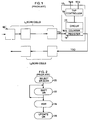
- FIG. 1 there is shown a block schematic diagram of a prior-art device 10 which is to be tested using boundary-scan techniques.
- the device 10 (hereinafter referred to as the device under test) is typically an active device, such as a memory or a microprocessor or the like, having at least one circuit 12 therein to which input and output connections are made via a set of input/output pins (not shown).
- test data register 14 Associated with the circuit 12 within the device 10 is a register 14, referred to as the test data register, which is provided within the circuit to facilitate boundary scan testing thereof in accordance with the procedure outlined in IEEE STD P1149.1, described in the document Standard Test Access Port and Boundary-Scan Architecture, sponsored by the Test Technology Committee of the IEEE Computer Society.
- the circuit 12 within the device 10, as well as the circuit within each of the other devices 10', may take various forms.
- the circuit 12 is assumed to be a memory (e.g., a RAM).
- an address counter 16 which serves to retain a value indicative of the location within the memory which is to store data, or from which data is to be read.
- Test Access Port controller (TAP) 18 whose details are discussed in the previously-mentioned Standard Test Access Port and Boundary-Scan Architecture document.
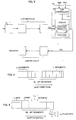
- the TAP controller 18 Among the operations controlled by the TAP controller 18 is the shift operation during which bits in a data stream are shifted through the device 10 and the devices 10′ in the same serial chain. For purposes of discussion, the operation of the TAP controller 18 will be described assuming that (L 1 + L + L 2 ) bits are to be shifted through the device 10 and the devices 10′ which are upstream and downstream therefrom. Referring now to FIG. 2, there is shown in flowchart form a summary or conceptual representation of steps executed by the TAP controller 18 of FIG. 1 to carry out shifting of data bits through the chain of devices 10.
- the first step (step 20) undertaken by the TAP controller 18 of FIG. 1 is to select the data register scan (shift) operation.
- Step 20 is initiated when the TAP controller 18 of FIG. 1 is supplied with a Test Mode Select (TMS) signal of a particular sequence.
- TMS Test Mode Select
- the TAP controller 18 causes the actual shifting of data (step 24).
- a successive one of the bits in the stream of test bits is shifted into a successive one of the cells in the register 14 in the boundary-scan chain in response to a successive "tick" (i.e., alternation of a periodic clock signal TCK input to the TAP controller 18).
- TMS Test Mode Select
- the shift step 22 is repeatedly executed to shift each of the bits in the stream of test bits (L 1 + L + L 2 ) into a separate one of the (L 1 + L + L 2 ) cells in the chain of devices 10 and 10′.
- the shifting operation is exited (step 24) whereupon an update operation (step 26) is executed during which the bit in each cell of each test data register 14 is applied to the corresponding input/output pin of the circuit 12 of FIG. 1.
- Efficient data transfer to and from the device under test 10 may be accomplished by modifying the device, as shown in FIG. 3, to incorporate a down-counter 28 which is controlled by the TAP controller 18.
- the counter 28 which is initially loaded with the value L 1 , is decremented each time a successive bit of the data stream is shifted into a successive one of the boundary-scan cells 16 in the boundary-scan chain of devices 10.
- the purpose in counting the first L 1 set of shift operations is to determine when the first L 1 bits in the data block (L 1 + NL) have been shifted into the L boundary-scan cells of the test data registers 14 in the devices 10' upstream of the test data in the device under test 10 so as to flush the data previously contained in these upstream cells. Otherwise, the test data in the device under test 10 could be loaded with "old" (i.e., meaningless) data.
- NL successive shift operations are additionally carried out so that a separate one of the N L-bit segments L A ,L B ,L C ...L N of interest is successively loaded into the boundary-scan data register 14. Every L clock cycles, a successive one of the L-bit segments then loaded into the test data register 14 is applied to the circuit 12 or, alternatively, the circuit applies a new L-bit segment to the register.
- the first N L-bit segments of the data block (L 1 + NL) are thus successively unpacked and loaded into the test data register 14 so that data can be transferred thereto or therefrom.
- the last L 1 bits of the data block (L 1 + NL) are provided to assure that the block is sufficiently long enough so that the last segments of interest up to 'N' can be successfully loaded when the last of the L 1 + NL shift operations is completed.
- the instant data transfer scheme is far more efficient.
- N the total number of clock cycles required would be on the order of L 1 + NL.
- the prior art scheme would require N(L 1 + L + L 2 ) operations.
- data transfer can be accomplished more rapidly.
- the instant data transfer technique while described for transferring data to a single test data register 14, can easily be employed to transfer data to multiple test data registers within the scan chain comprised of the device 10 under test and the devices 10' upstream and downstream therefrom.
- To efficiently transfer data to multiple test data registers 14 in a scan chain it would be necessary to concatenate the NL-bit segments to be transferred to each register behind the data block to be transferred to the register downstream therefrom.
- the counter 28 associated with each test data register 14 would have to be loaded with the appropriate value based on the number of scan cells in the test data registers upstream therefrom.
- the unpacking of a stream of bits of the form (L 1 + NL) can be achieved by controlling the manner in which the information from the test data register 14 is entered into the circuit 12, which, as previously indicated, is assumed to be a memory.
- the address counter 16 for storing the address of the location in the memory into which data is to be written or from which data is to be read.
- the address counter 16 associated with the memory circuit 12 operates to count upward from the lowest memory address to the highest and then freeze at the highest value. Assuming that the memory 12 is comprised of 256 words (i.e., storage locations), the address register 16, once it has addressed the 256th word, would retain the address of that word. To efficiently load the circuit 12 with data from the test data register 14, control of the address counter 16 is altered, through a program instruction, so that the address register "wraps around,” that is to say, it automatically returns to zero after addressing the 256th word.
- the stream of data entered to the boundary-scan chain was obtained by concatenating N separate L-bit segments to, and ahead of, a stream of L 1 filler bits.
- a slightly different data stream format is necessary, in the absence of the counter 28 of FIG. 3, to accomplish efficient data transfer.
- the data stream required for efficient data transfer contains an initial group of L ⁇ L 1 /L ⁇ - L 1 filler bits of don't care value.
- the reason for providing such a group of bits at the head of the data stream of interest is to ensure that the bits previously existing in the L 1 upstream boundary-scan cells in the boundary-scan chain of devices 10', together with the group of L ⁇ L 1 /L ⁇ - L 1 filler bits, comprises an integral number of L-bit segments.
- a block of N successive L-bit segments containing the data of interest is concatenated thereto, such that the first L ⁇ L 1 /L ⁇ bits in the block of NL bits lies at the end of the block.
- the reason for placing the first packet of L ⁇ L 1 /L ⁇ bits at the end of the block of NL bits will become better understood below.
- the TAP controller 18 of FIG. 1 To load the bit stream of (L 1 + NL + L ⁇ L 1 /L ⁇ - L 1 ), the TAP controller 18 of FIG. 1 enters its SHIFT state and commences the operations described in FIG. 3. As the shift operation 22 of FIG. 3 is successively carried out, the bits in the block (L 1 + NL + L ⁇ L 1 /L ⁇ - L 1 ) are unpacked by the device under test 10. Since the first packet of L ⁇ L 1 /L ⁇ bits in the block are don't care values, the first ⁇ L 1 /L ⁇ storage locations in the memory circuit 12 will be filled with filler bits.
- the next N - ⁇ L 1 /L ⁇ segments which contain valid data will be properly stored in the corresponding locations in the memory circuit 12 in accordance with address information in the address register 15 of FIG. 1.
- the value in the address register 15 wraps around to its lowest address value (zero) so that the initial ⁇ L 1 /L ⁇ segments in the memory circuit 12 are written over with valid data.
- the reason for placing the initial packet of ⁇ L 1 /L ⁇ segments in the data block of N L-bit segments is to compensate for the presence of L 1 scan cells of FIG. 1 in the devices 10' upstream of the device under test 10.
Landscapes
- Engineering & Computer Science (AREA)
- General Engineering & Computer Science (AREA)
- Physics & Mathematics (AREA)
- General Physics & Mathematics (AREA)
- Theoretical Computer Science (AREA)
- Computer Hardware Design (AREA)
- Quality & Reliability (AREA)
- Test And Diagnosis Of Digital Computers (AREA)
- Tests Of Electronic Circuits (AREA)
- Maintenance And Management Of Digital Transmission (AREA)
Applications Claiming Priority (2)
| Application Number | Priority Date | Filing Date | Title |
|---|---|---|---|
| US594516 | 1990-10-09 | ||
| US07/594,516 US5155732A (en) | 1990-10-09 | 1990-10-09 | Method and apparatus for data transfer to and from devices through a boundary-scan test access port |
Publications (3)
| Publication Number | Publication Date |
|---|---|
| EP0480619A2 EP0480619A2 (en) | 1992-04-15 |
| EP0480619A3 EP0480619A3 (ja) | 1994-02-23 |
| EP0480619B1 true EP0480619B1 (en) | 1996-07-10 |
Family
ID=24379213
Family Applications (1)
| Application Number | Title | Priority Date | Filing Date |
|---|---|---|---|
| EP91309018A Expired - Lifetime EP0480619B1 (en) | 1990-10-09 | 1991-10-02 | Methods for data transfer to and from devices through a boundary-scan test access port |
Country Status (5)
| Country | Link |
|---|---|
| US (1) | US5155732A (ja) |
| EP (1) | EP0480619B1 (ja) |
| JP (1) | JPH0731614B2 (ja) |
| KR (1) | KR920009113A (ja) |
| DE (1) | DE69120765T2 (ja) |
Families Citing this family (23)
| Publication number | Priority date | Publication date | Assignee | Title |
|---|---|---|---|---|
| US5254942A (en) * | 1991-04-25 | 1993-10-19 | Daniel D'Souza | Single chip IC tester architecture |
| JP2973641B2 (ja) * | 1991-10-02 | 1999-11-08 | 日本電気株式会社 | Tapコントローラ |
| US5377198A (en) * | 1991-11-27 | 1994-12-27 | Ncr Corporation (Nka At&T Global Information Solutions Company | JTAG instruction error detection |
| US5231314A (en) * | 1992-03-02 | 1993-07-27 | National Semiconductor Corporation | Programmable timing circuit for integrated circuit device with test access port |
| TW253097B (ja) * | 1992-03-02 | 1995-08-01 | At & T Corp | |
| DE4232271C1 (de) * | 1992-09-25 | 1994-02-17 | Siemens Ag | Elektronischer Baustein mit einer Schieberegisterprüfarchitektur (Boundary-Scan) |
| US5404526A (en) * | 1992-10-20 | 1995-04-04 | Dosch; Daniel G. | Improved method for accessing machine state information |
| US5448576A (en) * | 1992-10-29 | 1995-09-05 | Bull Hn Information Systems Inc. | Boundary scan architecture extension |
| US5333139A (en) * | 1992-12-30 | 1994-07-26 | Intel Corporation | Method of determining the number of individual integrated circuit computer chips or the like in a boundary scan test chain and the length of the chain |
| US5379302A (en) * | 1993-04-02 | 1995-01-03 | National Semiconductor Corporation | ECL test access port with low power control |
| US5490151A (en) * | 1993-07-26 | 1996-02-06 | At&T Corp. | Boundary scan cell |
| US6006343A (en) * | 1993-07-30 | 1999-12-21 | Texas Instruments Incorporated | Method and apparatus for streamlined testing of electrical circuits |
| US5544174A (en) * | 1994-03-17 | 1996-08-06 | The United States Of America As Represented By The Secretary Of The Air Force | Programmable boundary scan and input output parameter device for testing integrated circuits |
| US5513189A (en) * | 1994-05-25 | 1996-04-30 | Tandem Computers, Incorporated | Boundary scan system with improved error reporting using sentinel bit patterns |
| JP3849884B2 (ja) * | 1995-06-09 | 2006-11-22 | 富士通株式会社 | 2進数の1つのシーケンスを生成する装置、記憶モジュール内の障害に対するテストを行う方法、および記憶モジュールに対するテストを行うシステム |
| KR100240662B1 (ko) * | 1997-09-25 | 2000-01-15 | 윤종용 | 제이태그에 의한 다이나믹램 테스트장치 |
| US6032279A (en) * | 1997-11-07 | 2000-02-29 | Atmel Corporation | Boundary scan system with address dependent instructions |
| US6308290B1 (en) | 1999-05-20 | 2001-10-23 | International Business Machines Corporation | Look ahead scan chain diagnostic method |
| DE10032256C2 (de) * | 2000-07-03 | 2003-06-05 | Infineon Technologies Ag | Chip-ID-Register-Anordnung |
| US7188277B2 (en) * | 2003-03-28 | 2007-03-06 | Hewlett-Packard Development Company, L.P. | Integrated circuit |
| US7206983B2 (en) * | 2005-03-31 | 2007-04-17 | Lsi Logic Corporation | Segmented addressable scan architecture and method for implementing scan-based testing of integrated circuits |
| WO2010035238A1 (en) * | 2008-09-26 | 2010-04-01 | Nxp B.V. | Method for testing a partially assembled multi-die device, integrated circuit die and multi-die device |
| TWI640996B (zh) * | 2017-12-21 | 2018-11-11 | 新唐科技股份有限公司 | 記憶體電路及其測試方法 |
Family Cites Families (6)
| Publication number | Priority date | Publication date | Assignee | Title |
|---|---|---|---|---|
| JPS5864844A (ja) * | 1981-10-15 | 1983-04-18 | Victor Co Of Japan Ltd | 同期検出方式 |
| US4534028A (en) * | 1983-12-01 | 1985-08-06 | Siemens Corporate Research & Support, Inc. | Random testing using scan path technique |
| US4872169A (en) * | 1987-03-06 | 1989-10-03 | Texas Instruments Incorporated | Hierarchical scan selection |
| US4827476A (en) * | 1987-04-16 | 1989-05-02 | Tandem Computers Incorporated | Scan test apparatus for digital systems having dynamic random access memory |
| US4947357A (en) * | 1988-02-24 | 1990-08-07 | Stellar Computer, Inc. | Scan testing a digital system using scan chains in integrated circuits |
| US5079725A (en) * | 1989-11-17 | 1992-01-07 | Ibm Corporation | Chip identification method for use with scan design systems and scan testing techniques |
-
1990
- 1990-10-09 US US07/594,516 patent/US5155732A/en not_active Expired - Lifetime
-
1991
- 1991-10-02 DE DE69120765T patent/DE69120765T2/de not_active Expired - Fee Related
- 1991-10-02 EP EP91309018A patent/EP0480619B1/en not_active Expired - Lifetime
- 1991-10-07 JP JP3285417A patent/JPH0731614B2/ja not_active Expired - Fee Related
- 1991-10-08 KR KR1019910017570A patent/KR920009113A/ko not_active Application Discontinuation
Also Published As
| Publication number | Publication date |
|---|---|
| DE69120765T2 (de) | 1996-11-28 |
| EP0480619A2 (en) | 1992-04-15 |
| DE69120765D1 (de) | 1996-08-14 |
| EP0480619A3 (ja) | 1994-02-23 |
| JPH04263335A (ja) | 1992-09-18 |
| KR920009113A (ko) | 1992-05-28 |
| US5155732A (en) | 1992-10-13 |
| JPH0731614B2 (ja) | 1995-04-10 |
Similar Documents
| Publication | Publication Date | Title |
|---|---|---|
| EP0480619B1 (en) | Methods for data transfer to and from devices through a boundary-scan test access port | |
| US6049901A (en) | Test system for integrated circuits using a single memory for both the parallel and scan modes of testing | |
| US3940601A (en) | Apparatus for locating faults in a working storage | |
| US4404519A (en) | Testing embedded arrays in large scale integrated circuits | |
| US4754215A (en) | Self-diagnosable integrated circuit device capable of testing sequential circuit elements | |
| JP2636839B2 (ja) | デジタル集積回路 | |
| US4553090A (en) | Method and apparatus for testing a logic circuit using parallel to serial and serial to parallel conversion | |
| EP0160789B1 (en) | Test pattern generator | |
| JPH04212796A (ja) | 欠陥を許容できるシリアルメモリ | |
| JPH04278475A (ja) | 先読みパターン発生及びシミュレーションの方法及びシステム | |
| CN101297207A (zh) | Ic测试方法及设备 | |
| KR100690941B1 (ko) | 미리 기억된 가중치를 사용하는 가중치 랜덤 패턴 시험 | |
| WO1997011381A1 (fr) | Controleur de memoire | |
| US6594789B2 (en) | Input data capture boundary cell connected to target circuit output | |
| JP3987585B2 (ja) | コアのテスト制御 | |
| US5754758A (en) | Serial memory interface using interlaced scan | |
| US5305329A (en) | Delay data setting circuit and method | |
| JP3384272B2 (ja) | フェイルメモリ | |
| SU1429121A1 (ru) | Устройство дл формировани тестов | |
| JPH04221781A (ja) | 検査方法及び回路 | |
| US20020053055A1 (en) | Semiconductor device having a test mode | |
| US20050289421A1 (en) | Semiconductor chip | |
| Liu et al. | Techniques to reduce data volume and application time for transition test | |
| US6560289B1 (en) | Multi-tick transmission line and data storage element | |
| JP2867930B2 (ja) | 半導体装置 |
Legal Events
| Date | Code | Title | Description |
|---|---|---|---|
| PUAI | Public reference made under article 153(3) epc to a published international application that has entered the european phase |
Free format text: ORIGINAL CODE: 0009012 |
|
| AK | Designated contracting states |
Kind code of ref document: A2 Designated state(s): DE FR GB IT NL |
|
| PUAL | Search report despatched |
Free format text: ORIGINAL CODE: 0009013 |
|
| AK | Designated contracting states |
Kind code of ref document: A3 Designated state(s): DE FR GB IT NL |
|
| RAP3 | Party data changed (applicant data changed or rights of an application transferred) |
Owner name: AT&T CORP. |
|
| 17P | Request for examination filed |
Effective date: 19940811 |
|
| 17Q | First examination report despatched |
Effective date: 19950327 |
|
| GRAH | Despatch of communication of intention to grant a patent |
Free format text: ORIGINAL CODE: EPIDOS IGRA |
|
| GRAH | Despatch of communication of intention to grant a patent |
Free format text: ORIGINAL CODE: EPIDOS IGRA |
|
| GRAA | (expected) grant |
Free format text: ORIGINAL CODE: 0009210 |
|
| AK | Designated contracting states |
Kind code of ref document: B1 Designated state(s): DE FR GB IT NL |
|
| ITF | It: translation for a ep patent filed |
Owner name: JACOBACCI & PERANI S.P.A. |
|
| ET | Fr: translation filed | ||
| REF | Corresponds to: |
Ref document number: 69120765 Country of ref document: DE Date of ref document: 19960814 |
|
| PLBE | No opposition filed within time limit |
Free format text: ORIGINAL CODE: 0009261 |
|
| STAA | Information on the status of an ep patent application or granted ep patent |
Free format text: STATUS: NO OPPOSITION FILED WITHIN TIME LIMIT |
|
| 26N | No opposition filed | ||
| PGFP | Annual fee paid to national office [announced via postgrant information from national office to epo] |
Ref country code: NL Payment date: 20000925 Year of fee payment: 10 |
|
| PGFP | Annual fee paid to national office [announced via postgrant information from national office to epo] |
Ref country code: FR Payment date: 20010925 Year of fee payment: 11 |
|
| PGFP | Annual fee paid to national office [announced via postgrant information from national office to epo] |
Ref country code: GB Payment date: 20011008 Year of fee payment: 11 |
|
| PGFP | Annual fee paid to national office [announced via postgrant information from national office to epo] |
Ref country code: DE Payment date: 20011230 Year of fee payment: 11 |
|
| REG | Reference to a national code |
Ref country code: GB Ref legal event code: IF02 |
|
| PG25 | Lapsed in a contracting state [announced via postgrant information from national office to epo] |
Ref country code: NL Free format text: LAPSE BECAUSE OF NON-PAYMENT OF DUE FEES Effective date: 20020501 |
|
| NLV4 | Nl: lapsed or anulled due to non-payment of the annual fee |
Effective date: 20020501 |
|
| PG25 | Lapsed in a contracting state [announced via postgrant information from national office to epo] |
Ref country code: GB Free format text: LAPSE BECAUSE OF NON-PAYMENT OF DUE FEES Effective date: 20021002 |
|
| PG25 | Lapsed in a contracting state [announced via postgrant information from national office to epo] |
Ref country code: DE Free format text: LAPSE BECAUSE OF NON-PAYMENT OF DUE FEES Effective date: 20030501 |
|
| GBPC | Gb: european patent ceased through non-payment of renewal fee |
Effective date: 20021002 |
|
| PG25 | Lapsed in a contracting state [announced via postgrant information from national office to epo] |
Ref country code: FR Free format text: LAPSE BECAUSE OF NON-PAYMENT OF DUE FEES Effective date: 20030630 |
|
| REG | Reference to a national code |
Ref country code: FR Ref legal event code: ST |
|
| PG25 | Lapsed in a contracting state [announced via postgrant information from national office to epo] |
Ref country code: IT Free format text: LAPSE BECAUSE OF NON-PAYMENT OF DUE FEES;WARNING: LAPSES OF ITALIAN PATENTS WITH EFFECTIVE DATE BEFORE 2007 MAY HAVE OCCURRED AT ANY TIME BEFORE 2007. THE CORRECT EFFECTIVE DATE MAY BE DIFFERENT FROM THE ONE RECORDED. Effective date: 20051002 |