EP0473407A1 - Halbleiterbauelement mit einer getrennten aktiven Zone - Google Patents
Halbleiterbauelement mit einer getrennten aktiven Zone Download PDFInfo
- Publication number
- EP0473407A1 EP0473407A1 EP91307871A EP91307871A EP0473407A1 EP 0473407 A1 EP0473407 A1 EP 0473407A1 EP 91307871 A EP91307871 A EP 91307871A EP 91307871 A EP91307871 A EP 91307871A EP 0473407 A1 EP0473407 A1 EP 0473407A1
- Authority
- EP
- European Patent Office
- Prior art keywords
- region
- semiconductor device
- accordance
- bipolar transistor
- diffused
- Prior art date
- Legal status (The legal status is an assumption and is not a legal conclusion. Google has not performed a legal analysis and makes no representation as to the accuracy of the status listed.)
- Withdrawn
Links
- 239000004065 semiconductor Substances 0.000 title claims abstract description 33
- 239000012535 impurity Substances 0.000 claims abstract description 29
- 238000009792 diffusion process Methods 0.000 claims description 22
- VYPSYNLAJGMNEJ-UHFFFAOYSA-N Silicium dioxide Chemical compound O=[Si]=O VYPSYNLAJGMNEJ-UHFFFAOYSA-N 0.000 claims description 18
- 238000002955 isolation Methods 0.000 claims description 17
- 229910021420 polycrystalline silicon Inorganic materials 0.000 claims description 10
- 229920005591 polysilicon Polymers 0.000 claims description 10
- 229910052814 silicon oxide Inorganic materials 0.000 claims description 6
- 239000000758 substrate Substances 0.000 abstract description 16
- 235000014786 phosphorus Nutrition 0.000 description 33
- OAICVXFJPJFONN-UHFFFAOYSA-N Phosphorus Chemical compound [P] OAICVXFJPJFONN-UHFFFAOYSA-N 0.000 description 32
- 229910052698 phosphorus Inorganic materials 0.000 description 32
- 239000011574 phosphorus Substances 0.000 description 32
- ZOXJGFHDIHLPTG-UHFFFAOYSA-N Boron Chemical compound [B] ZOXJGFHDIHLPTG-UHFFFAOYSA-N 0.000 description 24
- 229910052796 boron Inorganic materials 0.000 description 24
- 230000000052 comparative effect Effects 0.000 description 21
- 238000005468 ion implantation Methods 0.000 description 19
- 229910052787 antimony Inorganic materials 0.000 description 14
- WATWJIUSRGPENY-UHFFFAOYSA-N antimony atom Chemical compound [Sb] WATWJIUSRGPENY-UHFFFAOYSA-N 0.000 description 14
- 238000000034 method Methods 0.000 description 13
- XUIMIQQOPSSXEZ-UHFFFAOYSA-N Silicon Chemical compound [Si] XUIMIQQOPSSXEZ-UHFFFAOYSA-N 0.000 description 12
- 238000005530 etching Methods 0.000 description 12
- XHXFXVLFKHQFAL-UHFFFAOYSA-N phosphoryl trichloride Chemical compound ClP(Cl)(Cl)=O XHXFXVLFKHQFAL-UHFFFAOYSA-N 0.000 description 12
- 229910052710 silicon Inorganic materials 0.000 description 12
- 239000010703 silicon Substances 0.000 description 12
- 229910052581 Si3N4 Inorganic materials 0.000 description 10
- HQVNEWCFYHHQES-UHFFFAOYSA-N silicon nitride Chemical compound N12[Si]34N5[Si]62N3[Si]51N64 HQVNEWCFYHHQES-UHFFFAOYSA-N 0.000 description 10
- 239000013078 crystal Substances 0.000 description 7
- 229910019213 POCl3 Inorganic materials 0.000 description 6
- 230000007547 defect Effects 0.000 description 6
- 235000012239 silicon dioxide Nutrition 0.000 description 6
- 239000000377 silicon dioxide Substances 0.000 description 6
- 230000005540 biological transmission Effects 0.000 description 5
- 238000005259 measurement Methods 0.000 description 5
- 230000003647 oxidation Effects 0.000 description 5
- 238000007254 oxidation reaction Methods 0.000 description 5
- IJGRMHOSHXDMSA-UHFFFAOYSA-N Atomic nitrogen Chemical compound N#N IJGRMHOSHXDMSA-UHFFFAOYSA-N 0.000 description 4
- 239000012299 nitrogen atmosphere Substances 0.000 description 4
- 230000015572 biosynthetic process Effects 0.000 description 3
- 238000001312 dry etching Methods 0.000 description 3
- 238000010438 heat treatment Methods 0.000 description 3
- QVGXLLKOCUKJST-UHFFFAOYSA-N atomic oxygen Chemical compound [O] QVGXLLKOCUKJST-UHFFFAOYSA-N 0.000 description 2
- 239000012159 carrier gas Substances 0.000 description 2
- 239000007789 gas Substances 0.000 description 2
- 229910052757 nitrogen Inorganic materials 0.000 description 2
- 239000001301 oxygen Substances 0.000 description 2
- 229910052760 oxygen Inorganic materials 0.000 description 2
- 238000012986 modification Methods 0.000 description 1
- 230000004048 modification Effects 0.000 description 1
Images


Classifications
-
- H—ELECTRICITY
- H10—SEMICONDUCTOR DEVICES; ELECTRIC SOLID-STATE DEVICES NOT OTHERWISE PROVIDED FOR
- H10D—INORGANIC ELECTRIC SEMICONDUCTOR DEVICES
- H10D62/00—Semiconductor bodies, or regions thereof, of devices having potential barriers
- H10D62/10—Shapes, relative sizes or dispositions of the regions of the semiconductor bodies; Shapes of the semiconductor bodies
- H10D62/124—Shapes, relative sizes or dispositions of the regions of semiconductor bodies or of junctions between the regions
-
- H—ELECTRICITY
- H10—SEMICONDUCTOR DEVICES; ELECTRIC SOLID-STATE DEVICES NOT OTHERWISE PROVIDED FOR
- H10D—INORGANIC ELECTRIC SEMICONDUCTOR DEVICES
- H10D10/00—Bipolar junction transistors [BJT]
- H10D10/40—Vertical BJTs
- H10D10/421—Vertical BJTs having both emitter-base and base-collector junctions ending at the same surface of the body
-
- H—ELECTRICITY
- H10—SEMICONDUCTOR DEVICES; ELECTRIC SOLID-STATE DEVICES NOT OTHERWISE PROVIDED FOR
- H10D—INORGANIC ELECTRIC SEMICONDUCTOR DEVICES
- H10D62/00—Semiconductor bodies, or regions thereof, of devices having potential barriers
- H10D62/10—Shapes, relative sizes or dispositions of the regions of the semiconductor bodies; Shapes of the semiconductor bodies
- H10D62/124—Shapes, relative sizes or dispositions of the regions of semiconductor bodies or of junctions between the regions
- H10D62/126—Top-view geometrical layouts of the regions or the junctions
Definitions
- the present invention relates to a semiconductor device, and more specifically to a silicon semiconductor device.
- an impurity diffused region has been formed without being divided, regardless of the size of the inpurity diffused region.
- the lattice constant of the impurity diffused region has deviated from an inherent lattice constant of a silicon crystal. If a crystal strain caused by the deviation of the lattice constant exceeds an elastic limit of the silicon, crystal defect (misfit dislocation) occurs in the impurity diffused region and on the periphery of the impurity diffused region. This is well known to persons skilled in the art. For example, it was reported in Journal of Applied Physics, Vol.
- misfit dislocation occurred in the case of diffusing P2O5 at 1000°C for 15 minutes so as to obtain a phosphorus concentration of 3x10²² atoms/cm3 at a wafer surface. If this misfit dislocation penetrates an emitter-base junction and a base-collector junction of a bipolar transistor and a drain region and a source region of a MOS transistor, it becomes a cause for a junction leakage. Therefore, it has been a conventional practice to set the impurity diffusion concentration at a level which does not allow the misfit to occur.
- the impurity concentration has been restrained to prevent misfits which would otherwise occur in a surface of the diffused region because the impurity concentration becomes very high at the surface of the diffused region. As a result, it has not been possible to sufficiently reduce the resistance of the diffused region.
- Another object of the present invention is to provide a semiconductor device having an impurity diffused region of a reduced resistance without crystal defect and therefore without leakage which would be caused by the crystal defect.
- a semiconductor device having an active region formed of an impurity diffused region which is divided into a plurality of impurity diffused sub-regions separated from each other but electrically coupled to each other.
- each of impurity diffused sub-regions is smaller than the impurity diffused region in the prior art, no misfit dislocation occurs. Therefore, the impurity diffused sub-regions can be diffused with impurities to a degree of concentration which is higher than the impurity concentration of the conventional semiconductor device. Accordingly, the resistance of the impurity diffused region can be sufficiently reduced.
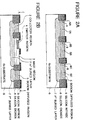
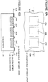
- FIG. 1 there is shown a diagrammatic plan view of a first embodiment of the semiconductor device in accordance with the present invention.
- Figures 2A and 2B are diagrammatic sectional views taken along the line IIA-IIA and the line IIB-IIB in Figure 1, respectively.
- the first embodiment includes a silicon substrate 6 including a boron diffused region 5 formed for electric contact for the substrate, the boron diffused region 5 being divided into a plurality of boron diffused sub-regions 5A, 5B and 5C by a device isolation silicon dioxide 1.
- the first embodiment was manufactured as follows: Arsenics (As) were selectively doped in one portion of a P-type silicon substrate 6 having a specific resistance of 10 ⁇ cm so as to form an n+ buried layer 11 having the concentration of 5x10¹⁹ atoms/cm3, and borons (B) were selectively doped in another portion of the P-type silicon substrate 6 so as to form a p+ buried layer 7 having the concentration of 2x10¹⁸ atoms/cm3. Then, an n-type epitaxial layer having a thickness of 1 ⁇ m was grown, and a device isolation region 8 of silicon dioxide was formed by using a conventional fine etching technology and a conventional selective oxidation technique. At this time, diffusion windows 8A for forming the boron diffused sub-regions 5A, 5B and 5C were formed by the device isolation region 8, as seen from figures 1, 2A and 2B.
- borons were ion-implanted at a dose of 6x 10¹⁵ atoms/cm2 through the boron diffused sub-region formation windows 8A, and then, a heat treatment was performed.
- the boron diffused sub-regions 5A, 5B and 5C were formed separately from each other as shown in Figures 1 and 2A.
- the boron diffused sub-regions 5A, 5B and 5C are electrically connected to each other since these sub-regions form the electric contact for the substrate.
- a collector region 2, a base region 3, and an emitter region 4 were formed as shown for example by using a mask formed in a silicon dioxide layer and a silicon nitride layer 9. Thus, a bipolar transistor was formed.
- FIGS 8, 9A and 9B two comparative examples of the bipolar transistor were formed in accordance with the same process for the first embodiment, except that the boron diffused region 5 was not divided.
- FIGs 8, 9A and 9B portions corresponding to those shown in Figures 1, 2A and 2B were given the same Reference Numerals, and explanation thereof will be omitted for simplification of description.
- the ion-implantation dose for the boron diffused region 5 was 1x10¹⁵ atoms/cm2 in a first one of the comparative examples, and 5x10¹⁵ atoms/cm2 in a second one of the comparative examples.
- the bipolar transistor in accordance with the first embodiment and the bipolar transistors in accordance with the prior art were examined by a transmission electron microscope so as to know occurrence of dislocations in the boron diffused region.
- the prior art bipolar transistor manufactured with the boron ion-implantation dose of 5x10¹⁵ atoms/cm2 57 dislocations occurred at average per a rectangular size of 3 ⁇ mx40 ⁇ m in the boron diffused region. Two dislocations at average of the found dislocations extended into the base region and/or the collector region.
- the bipolar transistor in accordance with the first embodiment and in the prior art bipolar transistor manufactured with the boron ion-implantation dose of 1x10¹⁵ atoms/cm2 no dislocation was found.
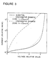
- FIG. 3 shows the result of the measurement. It would be understood that the bipolar transistor in accordance with the first embodiment has a leakage current, which is remarkably smaller than that of the prior art bipolar transistor manufactured with the boron ion-implantation dose of 5x10¹⁵ atoms/cm2, and which is comparable to that of the prior art bipolar transistor manufactured with the boron ion-implantation dose of 1x10¹⁵ atom/cm2.
- the resistance of the boron diffused region was measured.
- the resistance of the boron diffused region formed with the boron ion-implantation dose of 1x10¹⁵atoms/cm2 was about five times the resistance of the boron diffused region in the bipolar transistor in accordance with the first embodiment and the boron diffused region formed with the boron ion-implantation dose of 5x10¹⁵ atoms/cm2.
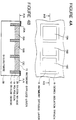
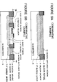
- FIG 4A there is shown a diagrammatic plan view of a second embodiment of the semiconductor device in accordance with the present invention.
- Figure 4B is a diagrammatic sectional views taken along the line IVB-IVB in figure 4A.
- the second embodiment is featured in that an antimony diffused region 15 is divided into a plurality of antimony diffused sub-regions by a device isolation trench 16.
- the second embodiment was manufactured as follows: In one portion of a P-type silicon substrate 29 having a specific resistance of 15 ⁇ cm, a device isolation trench 16 having a plan pattern as shown was formed by using a conventional fine etching technology, a conventional dry etching, and a polysilicon or silicon oxide growth technique. The device isolation trench 16 is coated with a silicon dioxide layer 18 and filled with a polysilicon 19. Then, an antimony diffusion window 20A was formed in a silicon oxide layer and a silicon nitride layer 20 by heat oxidation of the substrate surface, growth of silicon nitride, and a conventional fine etching technology.
- antimonies were ion-implanted at a dose of 5x10¹⁵ atoms/cm2 through the diffused sub-region formation windows 20A, and then, a heat treatment was performed at 1200°C under a nitrogen atmosphere for 5 hours.
- a plurality of antimony diffused sub-regions 15A, 15B and 15C were formed separately from each other by the device isolation trench 16, and an n+p junction diode was formed.
- the antimony diffused sub-regions 15A, 15B and 15C are electrically connected to each other.
- FIGS. 10A and 10B two comparative examples of the n+p junction diode were formed in accordance with the same process for the second embodiment, except that the antimony diffused region 15 was not divided.
- FIGS 10A and 10B portions corresponding to those shown in Figures 4A and 4B were given the same Reference Numerals, and explanation thereof will be omitted for simplification of description.
- the ion-implantation dose for the antimony diffused region 15 was 1x10¹⁵ atoms/cm2 in a first one of the comparative examples, and 5x10¹⁵ atoms/cm2 in a second one of the comparative examples.
- n+p diode in accordance with the second embodiment and the n+p diodes in accordance with the prior art were examined by a transmission electron microscope so as to know occurrence of dislocations in the antimony diffused region.
- n+p diode manufactured with the antimony ion-implantation dose of 5x10¹⁵ atoms/cm2 34 dislocations occurred at average per a rectangular size of 3 ⁇ mx15 ⁇ m in the antimony diffused region.
- no dislocation was found in the n+p diode in accordance with the second embodiment and in the prior art n+p diode manufactured with the antimony ion-implantation dose of 1x10¹⁵ atoms/cm2, no dislocation was found.
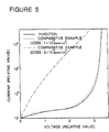
- Figure 5 shows the result of the measurement. It would be understood that the n+p diode in accordance with the second embodiment has a leakage current, which is remarkably smaller than that of the prior art n+p diode manufactured with the antimony ion-implantation dose of 5x10¹⁵ atoms/cm2, and which is comparable to that of the prior art n+p diode manufactured with the antimony ion-implantation dose of 1x10¹⁵ atoms/cm2.
- FIG. 6A there is shown a diagrammatic plan view of a third embodiment of the semiconductor device in accordance with the present invention.
- Figure 6B is a diagrammatic sectional views taken along the line VIB-VIB in figure 6A.
- the third embodiment is featured in that an phosphorus diffused region 21 is divided into a plurality of phosphorus diffused sub-regions.
- the third embodiment was manufactured as follows: On a P-type silicon substrate 22 having a specific resistance of 10 ⁇ cm, an phosphorus diffusion windovv 24A was formed by forming a silicon oxide layer 23 by heat oxidation of the substrate surface, by forming a silicon nitride layer 24 by growth of silicon nitride, and by selectively etching the stacked double layer by a conventional fine etching technology.
- phosphoruses were ion-implanted at a dose of 6x10¹⁵ atoms/cm2 through the diffused sub-region formation windovvs 24A, and then, a heat treatment was performed at 1100°C under a nitrogen atmosphere for 2 hours.
- a plurality of phosphorus diffused sub-regions 21A, 21B and 21C were formed separately from each other, and an n+p junction diode was formed.
- the phosphorus diffused sub-regions 21A, 21B and 21C are electrically connected to each other.
- FIG. 11 A and 11B two comparative examples of the n+p junction diode were formed in accordance with the same process for the third embodiment, except that the phosphorus diffused region 21 was not divided.
- FIG. 11A and 11B portions corresponding to those shown in figures 6A and 6B were given the same Reference Numerals,.and explanation thereof will be omitted for simplification of description.
- the ion-implantation dose for the phosphorus diffused region 21 was 1x10¹⁵ atoms/cm2 in a first one of the comparative examples, and 5x10¹⁵ atoms/cm2 in a second one of the comparative examples.
- n+p diode in accordance with the third embodiment and the n+p diodes in accordance with the prior art were examined by a transmission electron microscope so as to know occurrence of dislocations in the phosphorus diffused region.
- n+p diode manufactured with the phosphorus ion-implantation dose of 6x10¹⁵ atoms/cm2 37 dislocations occured at average per a rectangular size of 4 ⁇ mx10 ⁇ m the phosphorus diffused region.
- no dislocation was found in the n+p diode in accordance with the third embodiment and in the prior art n+p diode manufactured with the phosphorus ion-implantation dose of 1x10¹⁵ atoms/cm2, no dislocation was found.
- Figure 7 shows the result of the measurement. It would be understood that the n+p diode in accordance with the third embodiment has a leakage current, which is remarkably smaller than that of the prior art n+p diode manufactured with the phosphorus ion-implantation dose of 6x10¹⁵ atoms/cm2, and which is comparable to that of the prior art n+p diode manufactured with the phosphorus ion-implantation dose of 1x10¹⁵ atoms/cm2.
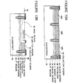
- FIG. 12 there is shown a diagrammatic plan view of a fourth embodiment of the semiconductor device in accordance with the present invention.
- Figures 13A and 13B are diagrammatic sectional views taken along the line XIIIA-XIIIA and the line XIIIB-XIIIB in Figure 12, respectively.
- the fourth embodiment is featured in that a collector region is divided into a plurality of collector sub-regions by a device isolation trench.
- the fourth embodiment was manufactured as follows: Arsenics (As) were selectively doped in one portion of a P-type silicon substrate 30 having a specific resistance of 10 ⁇ cm so as to form an n+ buried layer 32 having the concentration of 5x10¹⁹ atoms/cm3. Then, an n-type epitaxial layer having a thickness of 1 ⁇ m was grown, and a device isolation trench 34 was formed by a conventional fine etching technology, a conventional dry etching method and a conventional polysilicon growth technique. The device isolation trench 34 is coated with a silicon dioxide layer 36 and filled with a polysilicon 38. Under the device isolation trench 34, a stopper 40 of a p+ region is formed.
- a collector diffusion window was formed by forming a silicon oxide layer by heat oxidation of the substrate surface, by forming a silicon nitride layer 42 by growth of silicon nitride, and by selectively etching the stacked double layer by a conventional fine etching technology. Then, using a carrier gas composed of a mixed gas of nitrogen and oxygen and including 1000ppm of POCl3, diffusion was performed at 950°C for 15 minutes. In addition, phosphorus was further diffused at 1000°C under a nitrogen atmosphere for 20 minutes, so that a collector region 44 was formed. This collector region was divided into collector sub-regions 44A, 44B and 44C separately from each other by the device isolation trench 34. Thereafter, a base region 46 and an emitter region 48 were formed by an ion-implantation process. Similarly to the first embodiment, the collector sub-regions 44A, 44B and 44C are electrically connected to each other.
- the bipolar transistor in accordance with the fourth embodiment and the bipolar transistors in accordance with the prior art were examined by a transmission electron microscope so as to know occurrence of dislocations in the boron diffused region.
- 26 dislocations occurred at average per a rectangular size of 2 ⁇ mx20 ⁇ m in the collector region. Two dislocations at average of the found dislocations extended into the base region and the emitter region.
- no dislocation was found in the bipolar transistor in accordance with the fourth embodiment and in the prior art bipolar transistor manufactured with the phosphorus diffusion of 6 minutes.
- the bipolar transistor in accordance with the fourth embodiment had a cutoff frequency which was 1.3 times the cutoff frequency of the prior art bipolar transistor manufactured with the phosphorus diffusion of 6 minutes. This improvement of the cutoff frequency is considered to have been obtained because of the resistance of the collector region reduced without occurrence of dislocation in the collector region.
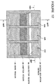
- FIG. 15 there is shown a diagrammatic plan view of a fifth embodiment of the semiconductor device in accordance with the present invention.
- Figures 16A and 16B are diagrammatic sectional views taken along the line XVIA-XVIA and the line XVIB-XVIB in Figure 15, respectively.
- the fifth embodiment is featured in that a collector region is divided into into plurality of collector sub-regions without using a device isolation trench.
- the fifth embodiment was manufactured as follows: Similarly to the fourth embodiment, arsenics (As) were selectively doped in one portion of a P-type silicon substrate 50 having a specific resistance of 10 ⁇ cm so as to form an n+ buried layer 52. Then, an n-type epitaxial layer having a thickness of 1 ⁇ m was grown, and a device isolation trench 54 was formed by a conventional fine etching technology, a conventional dry etching method and a conventional polysilicon growth technique. The device isolation trench 54 is coated with a silicon dioxide layer 56 and filled with a polysilicon 58. Under the device isolation trench 54, a stopper 60 of a p+ region is formed.
- a collector diffusion window was formed by forming a silicon oxide layer by heat oxidation of the substrate surface, by forming a silicon nitride layer by growth of silicon nitride, and by selectively etching the stacked double layer by a conventional fine etching technology.
- This collector diffusion window was into three in this fifth embodiment.
- a polysilicon layer 62 is formed on the collector diffusion window by growth of a polysilicon and a conventional fine etching technology. Then, using a carrier gas composed of a mixed gas of nitrogen and oxygen and including 1000ppm of POCl3, diffusion was performed at 950°C for 15 minutes. In addition, phosphorus was further diffused at 1000°C under a nitrogen atmosphere for 20 minutes, so that a collector region 64 was formed.
- This collector region was divided into collector sub-regions 64A, 64B and 64C separately from each other by the three collector diffusion windows. But, the collector sub-regions 64A, 64B and 64C are electrically connected to each other by the phosphorus diffused polysilicon layer 62. Thereafter, a base region 66 and an emitter region 68 were formed by an ion-implantation process, by utilizing for example a silicon nitride layer 70.
- FIGS 20A and 20B two comparative examples of the bipolar transistor were formed in accordance with the same process for the fifth embodiment, except that the collector region 64 was not divided.
- a plan view of these comparative examples is the same as Figure 18, and therefore, the plan view will be omitted.
- FIGs 20 and 20B portions corresponding to those shown in Figures 15, 16A and 16B were given the same Reference Numerals, and explanation thereof will be omitted for simplification of description.
- phosphorus was diffused by using 1000ppm of POCl3 at 950°C for 6 minutes, and in a second one of the comparative examples, phosphorus was diffused by using 1000ppm of POCl3 at 950°C for 15 minutes.
- the bipolar transistor in accordance with the fifth embodiment and the bipolar transistors in accordance with the prior art were examined by a transmission electron microscope so as to know occurrence of dislocations in the boron diffused region.
- 27 dislocations occurred at average per a rectangular size of 2 ⁇ mx20 ⁇ m in the collector region.
- Two dislocations at average of the found dislocations extended into the base region and the emitter region.
- no dislocation was found in the bipolar transistor in accordance with the fifth embodiment and in the prior art bipolar transistor manufactured with the phosphorus diffusion of 6 minutes.
- the bipolar transistor in accordance with the fifth embodiment has a leakage current which is remarquably smaller than that of the prior art bipolar transistor manufactured with the phosphorus diffusion of 15 minutes, and which is comparable to that of the prior art bipolar transistor manufactured with the phosphorus diffusion of 6 minutes.
- the cutoff frequency which is one index indicative of the high frequency operation performance of the bipolar transistor was measured.
- the bipolar transistor in accordance with the fifth embodiment had a cutoff frequency which was 1.2 times the cutoff frequency of the prior art bipolar transistor manufactured with the phosphorus diffusion of 6 minutes. This improvement of the cutoff frequency is considered to have been obtained because of the resistance of the collector region reduced without occurrence of dislocation in the collector region.
- the semiconductor device in accordance with the present invention has an impurity diffused region having a reduced resistance without crystal defect and therefore without leakage which would be caused by the crystal defect. Therefore, the semiconductor device in accordance with the present invention can operate at a high speed.
Landscapes
- Bipolar Transistors (AREA)
- Electrodes Of Semiconductors (AREA)
Applications Claiming Priority (2)
| Application Number | Priority Date | Filing Date | Title |
|---|---|---|---|
| JP22613290A JP3145694B2 (ja) | 1990-08-28 | 1990-08-28 | 半導体装置 |
| JP226132/90 | 1990-08-28 |
Publications (1)
| Publication Number | Publication Date |
|---|---|
| EP0473407A1 true EP0473407A1 (de) | 1992-03-04 |
Family
ID=16840351
Family Applications (1)
| Application Number | Title | Priority Date | Filing Date |
|---|---|---|---|
| EP91307871A Withdrawn EP0473407A1 (de) | 1990-08-28 | 1991-08-28 | Halbleiterbauelement mit einer getrennten aktiven Zone |
Country Status (3)
| Country | Link |
|---|---|
| US (1) | US5285101A (de) |
| EP (1) | EP0473407A1 (de) |
| JP (1) | JP3145694B2 (de) |
Families Citing this family (3)
| Publication number | Priority date | Publication date | Assignee | Title |
|---|---|---|---|---|
| JP3360970B2 (ja) * | 1995-05-22 | 2003-01-07 | 株式会社東芝 | 半導体装置の製造方法 |
| US5820736A (en) * | 1996-12-23 | 1998-10-13 | Bouziane; Richard | Pyrolysing apparatus |
| US6624031B2 (en) * | 2001-11-20 | 2003-09-23 | International Business Machines Corporation | Test structure and methodology for semiconductor stress-induced defects and antifuse based on same test structure |
Citations (8)
| Publication number | Priority date | Publication date | Assignee | Title |
|---|---|---|---|---|
| US3958267A (en) * | 1973-05-07 | 1976-05-18 | National Semiconductor Corporation | Current scaling in lateral pnp structures |
| US4202005A (en) * | 1978-11-20 | 1980-05-06 | Trw Inc. | Distributed collector ballast resistor structure |
| EP0029369A2 (de) * | 1979-11-20 | 1981-05-27 | Fujitsu Limited | Verfahren zur Herstellung einer Halbleitervorrichtung |
| FR2592526A1 (fr) * | 1985-12-31 | 1987-07-03 | Radiotechnique Compelec | Circuit integre comportant un transistor lateral |
| FR2601504A1 (fr) * | 1986-07-09 | 1988-01-15 | Radiotechnique Compelec | Dispositif semiconducteur comportant un transistor pour logique integree a injection |
| EP0322380A2 (de) * | 1987-12-22 | 1989-06-28 | STMicroelectronics S.r.l. | Verfahren, um die Kollektorfläche eines lateralen PNP Transistors differentiel zu vergrössern während des elektrischen Tests einer integrierten Schaltung auf einem Wafer |
| EP0328286A2 (de) * | 1988-02-11 | 1989-08-16 | Exar Corporation | Vertikaler PNP-Kielfachkollektortransistor |
| EP0337720A2 (de) * | 1988-04-11 | 1989-10-18 | Synergy Semiconductor Corporation | Herstellungsprozess für Hochleistungsbipolarstruktur |
Family Cites Families (3)
| Publication number | Priority date | Publication date | Assignee | Title |
|---|---|---|---|---|
| JPS6266672A (ja) * | 1985-09-19 | 1987-03-26 | Sharp Corp | 半導体装置 |
| JPH027529A (ja) * | 1988-06-27 | 1990-01-11 | Nec Corp | バイポーラトランジスタ及びその製造方法 |
| JP2894777B2 (ja) * | 1990-03-02 | 1999-05-24 | 日本電気株式会社 | 半導体装置 |
-
1990
- 1990-08-28 JP JP22613290A patent/JP3145694B2/ja not_active Expired - Fee Related
-
1991
- 1991-08-28 US US07/751,113 patent/US5285101A/en not_active Expired - Fee Related
- 1991-08-28 EP EP91307871A patent/EP0473407A1/de not_active Withdrawn
Patent Citations (8)
| Publication number | Priority date | Publication date | Assignee | Title |
|---|---|---|---|---|
| US3958267A (en) * | 1973-05-07 | 1976-05-18 | National Semiconductor Corporation | Current scaling in lateral pnp structures |
| US4202005A (en) * | 1978-11-20 | 1980-05-06 | Trw Inc. | Distributed collector ballast resistor structure |
| EP0029369A2 (de) * | 1979-11-20 | 1981-05-27 | Fujitsu Limited | Verfahren zur Herstellung einer Halbleitervorrichtung |
| FR2592526A1 (fr) * | 1985-12-31 | 1987-07-03 | Radiotechnique Compelec | Circuit integre comportant un transistor lateral |
| FR2601504A1 (fr) * | 1986-07-09 | 1988-01-15 | Radiotechnique Compelec | Dispositif semiconducteur comportant un transistor pour logique integree a injection |
| EP0322380A2 (de) * | 1987-12-22 | 1989-06-28 | STMicroelectronics S.r.l. | Verfahren, um die Kollektorfläche eines lateralen PNP Transistors differentiel zu vergrössern während des elektrischen Tests einer integrierten Schaltung auf einem Wafer |
| EP0328286A2 (de) * | 1988-02-11 | 1989-08-16 | Exar Corporation | Vertikaler PNP-Kielfachkollektortransistor |
| EP0337720A2 (de) * | 1988-04-11 | 1989-10-18 | Synergy Semiconductor Corporation | Herstellungsprozess für Hochleistungsbipolarstruktur |
Non-Patent Citations (3)
| Title |
|---|
| PATENT ABSTRACTS OF JAPAN vol. 10, no. 352 (E-458) 27 November 1986, & JP-A-61 152068 (HITACHI LTD.) 10 July 1986, * |
| PATENT ABSTRACTS OF JAPAN vol. 11, no. 257 (E-534) 20 August 1987, & JP-A-62 066672 (SHARP CORP.) 26 March 1987, * |
| PROCEEDINGS OF THE 1988 BIPOLAR CIRCUITS AND TECHNOLOGY MEETING 12 September 1988, MINNEAPOLIS, MINNESOTA pages 199 - 201; Lj. RISTIC et al.: "A CMOS bipolar transistor with a locally doped base in the proximity of the emitter as a magnetic field sensor" * |
Also Published As
| Publication number | Publication date |
|---|---|
| JP3145694B2 (ja) | 2001-03-12 |
| US5285101A (en) | 1994-02-08 |
| JPH04107829A (ja) | 1992-04-09 |
Similar Documents
| Publication | Publication Date | Title |
|---|---|---|
| US6218254B1 (en) | Method of fabricating a self-aligned bipolar junction transistor in silicon carbide and resulting devices | |
| US5620907A (en) | Method for making a heterojunction bipolar transistor | |
| US4507171A (en) | Method for contacting a narrow width PN junction region | |
| EP0274278A1 (de) | MOS-Feldeffekttransistor und dessen Herstellungsmethode | |
| EP0090940A2 (de) | Verfahren zum Herstellen von Emitter- und intrinsic-Basisgebieten eines bipolaren Transistors | |
| US3925120A (en) | A method for manufacturing a semiconductor device having a buried epitaxial layer | |
| EP0779664A2 (de) | Anordnung mit einem Heteroübergang-Bipolartransistor | |
| JPS62219636A (ja) | 半導体装置 | |
| KR970053503A (ko) | 게이트 전극 및 소스와 드레인 영역 사이의 단락을 없애는 얕은 불순물 영역을 구비한 반도체 디바이스 및 이를 제조하는 공정 | |
| US6087683A (en) | Silicon germanium heterostructure bipolar transistor with indium doped base | |
| US3299329A (en) | Semiconductor structures providing both unipolar transistor and bipolar transistor functions and method of making same | |
| US11158722B2 (en) | Transistors with lattice structure | |
| Burghartz et al. | Selective epitaxy base transistor (SEBT) | |
| EP0473407A1 (de) | Halbleiterbauelement mit einer getrennten aktiven Zone | |
| US6930011B2 (en) | Semiconductor device with a bipolar transistor, and method of manufacturing such a device | |
| US6642096B2 (en) | Bipolar transistor manufacturing | |
| US5504363A (en) | Semiconductor device | |
| US5506156A (en) | Method of fabricating bipolar transistor having high speed and MOS transistor having small size | |
| JP2652995B2 (ja) | 半導体装置およびその製造方法 | |
| US6740560B1 (en) | Bipolar transistor and method for producing same | |
| KR100293978B1 (ko) | 바이폴라트랜지스터및그제조방법 | |
| KR940001257B1 (ko) | 반도체 소자 제조방법 | |
| KR940010913B1 (ko) | 고내압 바이폴라 트랜지스터 및 그 제조방법 | |
| EP0600693A2 (de) | Selektives Grabenätzen und selbstausrichtende Basis-Emitter-Struktur | |
| JPS60137072A (ja) | 接合型電界効果トランジスタの製造方法 |
Legal Events
| Date | Code | Title | Description |
|---|---|---|---|
| PUAI | Public reference made under article 153(3) epc to a published international application that has entered the european phase |
Free format text: ORIGINAL CODE: 0009012 |
|
| 17P | Request for examination filed |
Effective date: 19910912 |
|
| AK | Designated contracting states |
Kind code of ref document: A1 Designated state(s): DE FR GB |
|
| 17Q | First examination report despatched |
Effective date: 19941103 |
|
| STAA | Information on the status of an ep patent application or granted ep patent |
Free format text: STATUS: THE APPLICATION IS DEEMED TO BE WITHDRAWN |
|
| 18D | Application deemed to be withdrawn |
Effective date: 19960802 |