EP0472357B1 - Integrierter Halbleiterschaltkreis - Google Patents
Integrierter Halbleiterschaltkreis Download PDFInfo
- Publication number
- EP0472357B1 EP0472357B1 EP91307502A EP91307502A EP0472357B1 EP 0472357 B1 EP0472357 B1 EP 0472357B1 EP 91307502 A EP91307502 A EP 91307502A EP 91307502 A EP91307502 A EP 91307502A EP 0472357 B1 EP0472357 B1 EP 0472357B1
- Authority
- EP
- European Patent Office
- Prior art keywords
- substrate
- integrated circuit
- gate
- conductive path
- monolithic integrated
- Prior art date
- Legal status (The legal status is an assumption and is not a legal conclusion. Google has not performed a legal analysis and makes no representation as to the accuracy of the status listed.)
- Expired - Lifetime
Links
Images







Classifications
-
- H—ELECTRICITY
- H10—SEMICONDUCTOR DEVICES; ELECTRIC SOLID-STATE DEVICES NOT OTHERWISE PROVIDED FOR
- H10D—INORGANIC ELECTRIC SEMICONDUCTOR DEVICES
- H10D84/00—Integrated devices formed in or on semiconductor substrates that comprise only semiconducting layers, e.g. on Si wafers or on GaAs-on-Si wafers
- H10D84/01—Manufacture or treatment
-
- H—ELECTRICITY
- H10—SEMICONDUCTOR DEVICES; ELECTRIC SOLID-STATE DEVICES NOT OTHERWISE PROVIDED FOR
- H10D—INORGANIC ELECTRIC SEMICONDUCTOR DEVICES
- H10D84/00—Integrated devices formed in or on semiconductor substrates that comprise only semiconducting layers, e.g. on Si wafers or on GaAs-on-Si wafers
- H10D84/01—Manufacture or treatment
- H10D84/02—Manufacture or treatment characterised by using material-based technologies
- H10D84/05—Manufacture or treatment characterised by using material-based technologies using Group III-V technology
-
- H—ELECTRICITY
- H10—SEMICONDUCTOR DEVICES; ELECTRIC SOLID-STATE DEVICES NOT OTHERWISE PROVIDED FOR
- H10W—GENERIC PACKAGES, INTERCONNECTIONS, CONNECTORS OR OTHER CONSTRUCTIONAL DETAILS OF DEVICES COVERED BY CLASS H10
- H10W20/00—Interconnections in chips, wafers or substrates
- H10W20/20—Interconnections within wafers or substrates, e.g. through-silicon vias [TSV]
Definitions
- the present invention relates to a semiconductor integrated circuit for processing a high frequency signal such as microwave signal, and more particularly to a structure of a microwave monolithic integrated circuit for preventing electrostatic breakdown in the fabricating process thereof.
- FIG 10 is a plan view showing a semiconductor integrated circuit of a high frequency switch as an example of a semiconductor integrated circuit utilizing a dielectric substrate in accordance with a prior art.
- reference character Q1 designates a field effect transistor (hereinafter referred to as 'FET') constructed on a dielectric substrate 1, which has a source S, a gate G, and a drain D.
- a first transmission line T1 is connected to the gate G of the FET Q1 and the electric length thereof is usually established at one fourth wavelength of the microwave signal, which enables impedance matching of the first transmission line T1 with the gate G.
- a capacitor C1 is connected to the first transmission line T1 and this is also connected to the grounding bonding pad P2.
- a gate bias bonding pad P1 is provided in contact with the node of the first transmission line T1 and the first capacitor C1.
- a second transmission line T2 is connected to the source S of the FET Q1.
- a via-hole V is provided for connecting the second transmission line T2 with a rear surface electrode 4 produced at the rear surface of the dielectric substrate 1.
- Reference characters M1 and M2 designate transmission lines connected to the source S and the drain D of the FET Q1, respectively.
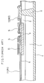
- Figure 11 is a cross sectional view showing the device of figure 10 and schematically shows the FET portion, the via-hole portion, and the connecting relation between these and the transmission lines T1 and T2.
- Figure 11 does not completely coincide with a plane pattern of figure 10.
- reference numeral 2 designates a semiconductor layer such as GaAs produced on a dielectric substrate 1 by such as epitaxial growth method.
- An operating layer 3 of the FET Q1 is produced in the semiconductor layer 2 by implanting n conductivity type impurities such as silicon using such as ion implantation method.
- a source electrode S and a drain electrode D are produced on the operating layer 3 and a gate electrode G is produced on the operating layer 3 between the both electrodes.
- an insulating substrate comprising such as sapphire or alumina is used for the dielectric substrate 1
- gold-germanium alloy is used for the source S and the drain D which are in ohmic contact with the operating layer 3
- aluminum is used for the gate electrode G which is in Schottky contact with the operating layer 3.
- the transmission lines M1, M2, T1, and T2 comprise metal material.
- Reference numeral 5 designates an insulating film on which the transmission lines T1 and T2 are produced.
- the other same reference numerals as those shown in figure 10 designate the same parts.
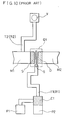
- Figure 12 shows an equivalent circuit of the above-described semiconductor integrated circuit.
- An RF input terminal 7 and an RF output terminal 8 are connected to the transmission lines M1 and M2, respectively.
- a gate bias voltage power supply 9 is corrected to the gate bias bonding pad P1.
- the other same reference numerals as those shown in figures 10 and 11 designate the same portions.
- a high frequency signal such as microwave signal is input to the RF input terminal 7, supplied to the FET Q1 through the transmission line M1, and output from the RF output terminal 8 through the transmission line M2.
- the transmission line T1 and the capacitor C1 form a gate bias circuit of the FET Q1, and in this example a voltage bias is applied to the gate G of the FET from the gate bias power supply 9 which is provided outside the dielectric substrate 1, through the gate bias bonding pad P1.
- the electrical length of the transmission line T1 is usually established at one fourth wavelength of the microwave signal and the end terminal of the transmission line T1 is grounded at a high frequency via the capacitor C1. Therefore, viewed at the gate of the FET Q1, the impedance of the transmission line T1 becomes infinite, which prevents the microwave signal from leaking to the gate G of the FET through the gate-source or the gate-drain capacitance of the FET Q1.
- a resistor R1 can be used instead of the transmission line T1.
- the value of the resistor R1, typically 1 K ⁇ which is sufficiently higher than characteristics impedance of the-transmission line M1, typically 50 ⁇ enables preventing the microwave signal from leaking to the gate G of the FET through the gate-source or gate-drain capacitance of the FET Q1.
- the resistor R1 can be made of a semiconductor layer or a thin film resistor.
- the capacitor C1 also prevents unrequired high frequency signal from being applied to the gate of the FET Q1 from outside of the dielectric substrate 1 through the gate bonding pad P1.
- the capacitor C1 is grounded at the rear surface electrode via the grounding bonding pad P2, it can be grounded inside the dielectric substrate 1 using a via-hole.
- the transmission line T2 produces a source voltage bias circuit of the FET Q1, and in this example, the source voltage bias circuit of the FET Q1 is grounded at the rear surface electrode 4.
- the electrical length of the transmission line T2 is established at one fourth wavelength of the microwave signal.
- the microwave signal is prevented from leaking to the transmission line T2 from the transmission line M1.
- a second resistor R2 is used in place of the transmission line T2
- establishing the value of the resistor R2 at a value, typically 1 k ⁇ , sufficiently higher than the characteristic impedance of the transmission line M1, typically 50 ⁇ enables preventing the leakage of the microwave signal.
- the attenuation quantity of the intensity of the microwave signal input from the RF input terminal 7 is controlled by varying the gate bias voltage of the FET Q1, more concretely by varying the drain-source resistance of the FET Q1 in a range from a sufficiently small value of several ⁇ to a sufficiently large value of several M ⁇ , thereby enabling taking out a signal from the RF output terminal 8.
- an electrical length of the transmission line T2 is established at one fourth wavelength, but a microwave switching circuit which can make the microwave signal input from the RF output terminal 8 grounded or opened at the FET Q1 can be obtained by directly grounding the source S of the FET Q1 with the transmission line T2 and the transmission line M1 dispensed with.
- Figure 13 is a plan view showing a semiconductor integrated circuit constituting a high frequency switch which is a prior art example of a semiconductor integrated circuit using a semi-insulating semiconductor substrate.
- Figure 14 is a cross sectional view thereof and this schematically shows the FET portion, the via-hole portion, and the connecting relation between these and the transmission lines T1 and T2.
- the same reference numerals as those shown in figures 10 and 11 designate the same portions.
- a semi-insulating semiconductor substrate 14 is used in place of the dielectric substrate in the semiconductor integrated circuit shown in figures 10 to 12 and the source S and the drain D of the FET Q1 are connected to the rear surface electrode 4 via the substrate resistor 6.
- the bias circuit of the source S is provided at the outside, the second transmission line T2 and the via-hole V are not used for connecting the source S to the rear surface electrode.
- Figure 15 shows an equivalent circuit of the semiconductor integrated circuit of figure 13.
- reference numeral 6 designates a substrate resistor between the source S, drain D and the rear surface electrode 4.
- the same reference numerals as those shown in figure 12 designate the same portions.
- a source bias is applied from outside of the semi-insulating semiconductor substrate 1 using a circuit construction for applying DC bias such as biastee .
- a substrate resistor 6 exists between the rear surface electrode 4 and the source S or the drain D of the FET as shown in figure 14, differently from the case of using a semi-insulating dielectric substrate such as sapphire substrate, and the value of this substrate resistor 6 is usually more than 1 M ⁇ . Therefore, the circuit operation is similar as that of the equivalent circuit of figure 12.
- the prior art semiconductor integrated circuit which has a construction as described above, where the gate of the FET Q1 is insulated from the source or the drain of the FET Q1 from a view point of DC, has a following problem. That is, in a process of fabricating a semiconductor integrated circuit such as a chip separation process, pure water which is blown to a wafer while cutting a semiconductor integrated circuit substrate by a dicing-saw causes the electrification of the gate bias circuit, that is, the electrification of the bonding pads for the gate, the source, and the drain which are not covered with passivation films, and this results an electrostatic breakdown of a gate.
- the resistance of the pn junction element is smaller than the serial resistance of the gate, the impedance at the gate changes and the impedance matching is not performed in the microwave circuit. As a result, a leakage or reflection of the transmitting microwave arises exerting unfavorable influence on the input side circuit.
- the present invention is directed to solving the above described problems and has for its object to provide a microwave monolithic integrated circuit that prevents the electrification of the gate bias circuit without arising impedance mismatching at the gate, and the destruction caused by the electrification of the gate of the FET in the gate fabrication process of a field effect transistor is prevented.
- static electricity charged to the gate bias bonding pad or the capacitor constituting the gate bias circuit in the fabrication process flows not through the gate of the FET but through the auxiliary current path, whereby the gate-can be protected from the electrostatic breakdown.
- Figure 1 shows a high frequency switch semiconductor integrated circuit as an example of semiconductor integrated circuit using a dielectric substrate in accordance with a first embodiment of the present invention.
- Figure 2 is a cross sectional view thereof showing the FET portion, the via-hole portion, and the connecting relation between these and the transmission lines T1 and T2.
- Figure 3 shows an equivalent circuit thereof.
- These figures 1 to 3 correspond to figures 10 to 12 which show a prior art example and the same reference numerals designate the same or corresponding portions.
- the first transmission line T1 is connected to the rear surface electrode via the third resistor R3 of about 100 K ⁇ .
- This resistor R3 has a sufficiently high resistance value,as described above and affects almost no influence on the gate bias circuit.
- a via-hole V1 is produced in the vicinity of the transmission line T1.
- a third resistor R3 comprising a refractory metal silicide layer such as nichrome (alloy of nickel and chrome), tungsten silicide, or molybdenum silicide, is produced on an insulating film 5 between the via-hole V and the transmission line T1.
- This resistor R3 is connected to the transmission line T1 at its one end and to the rear surface electrode 4 through the via-hole V at its other end.
- a GaAs semiconductor layer 2 is epitaxially grown on a wafer substrate 1 comprising such as sapphire, and subsequently n conductivity type impurity such as silicon is ion implanted into the GaAs semiconductor layer 2 to produce an operating layer 3 at a surface region of the semiconductor layer 2.
- a gold-germanium alloy layer is patterned on the operating layer 3 and a source S and a drain D are produced from the gold-germanium alloy layer. Thereafter, an aluminum layer is patterned to produce a gate G. Then, an electrode layer E comprising gold is produced at a position corresponding to the via-hole which is produced in the later process.
- an insulating film 5 is patterned on the entire surface, a third resistor layer R3 comprising the above described refractory metal silicide layer is patterned, and then a first and a second transmission lines T1 and T2, transmission lines M1 and M2, and gate bonding pads P1 and P2 all comprising metal material are produced. At this time, the capacitor C1 is also produced and portions other than the bonding pad portion are covered by a passivation film.
- the sapphire substrate 1 is etched back from the rear surface side to a predetermined thickness, a via-hole V is produced by etching, and further the entire surface is gilded by gold so as to bury the via-hole and produce a rear surface electrode 4.
- the wafer substrate is separated into chips by a dicing-saw.
- the semiconductor integrated circuit is devised so as to be able to suppress generation of static electricity in the fabrication process, there are some cases where sufficient countermeasure cannot be implemented.
- chip separation with a dicing-saw it is necessary to spray pure water to the dielectric substrate at a high pressure in order to wash out the dust generated by cutting.
- the pure water has high resistance and is likely to be charged, electrode portions such as an exposed bonding pad produced on the dielectric substrate is easily electrified by charges conveyed by the pure water.
- the drain D of the FET Q1 in this embodiment is not connected to the rear surface electrode 4 via such as a bias circuit
- the drain D of a normally-on type transistor which is a GaAs FET usually used for a microwave is connected to the source S through the operating layer 3, which means the drain D is grounded at the rear surface electrode 4 through the source S so that the drain D does not have a high voltage due to electrification, either.
- Electrostatic breakdown of the gate due to electrification in the fabrication process can be prevented because the gate G, the source S, and the drain D of the FET Q1 are grounded at the rear surface electrode directly or via the resistor.
- the source is grounded at the rear surface electrode through a second transmission line, not a source but a drain can be grounded. Furthermore, either the source or drain electrode can be grounded directly to the rear surface electrode not through the transmission line but through a via-hole which is produced directly below the source or the drain represented by broken lines in figure 2.
- the gate G and the capacitor C1 are connected by a first transmission line and the source S and the rear surface electrode 4 are connected by a second transmission line, respectively, but they can be connected by a first and a second resistors R1 and R2, respectively as explained in the prior art.
- Figure 4 to figure 6 show a second embodiment of the present invention.
- This second embodiment is a semiconductor integrated circuit constituting a high frequency switch using a semi-insulating semiconductor substrate.
- Figure 4 to figure 6 are a plan view, a cross sectional view, and an equivalent circuit diagram corresponding to figure 1 to figure 3, respectively.
- a semi-insulating semiconductor substrate 14 is used in place of the insulating dielectric substrate in the semiconductor integrated circuit of the first embodiment and the source S and the drain D of the FET Q1 are connected to the rear surface electrode via the substrate resistor 6. Further, since the bias circuit of the source S is provided at the outside, a second transmission line T2 and a via-hole V for connecting the source S to the rear surface electrode are not used.
- the gate G of the FET Q1 is grounded at the rear surface electrode 4 through the third resistor R3, therefore, the charges conveyed by such as pure water used for washing in the semiconductor fabrication process flow into the rear surface electrode through the third resistor so that the gate G does not have a high voltage due to electrification.
- the source S of the FET Q1 is not connected to the rear surface electrode 4 through the via-hole V differently from first embodiment, the semi-insulating semiconductor substrate 1 is used as a dielectric substrate and the source S and the drain D are grounded at the rear surface electrode 4 via the substrate resistor 6; therefore neither the source S nor the drain D has a high voltage due to electrification.
- Electrostatic breakdown of the gate caused by the electrification in the fabrication process can be prevented because the gate G, the source S, and the drain D of the FET Q1 are grounded at the rear surface electrode directly or via the resistor.
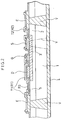
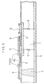
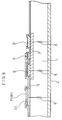
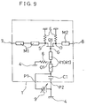
- FIG. 7 to figure 9 show a plan view, a cross sectional view, and an equivalent circuit diagram of a semiconductor integrated circuit in accordance with a third embodiment of the present invention, which correspond to figure 4 to figure 6, respectively.
- an ohmic electrode O1 is produced below a portion of the first transmission line T1 in the construction of the second embodiment, and thus the gate G and the rear surface electrode 4 are connected with each other.
- the ohmic electrode O1 has sufficiently large area so that the electric resistance between the gate G and the rear surface electrode 4 becomes as small as that of the substrate resistor 6.
- the other construction is the same as those of the second embodiment.
- the source S of the FET Q1 is not connected to the rear surface electrode 4 through the via-hole V.
- the source S and the drain D are connected to the rear surface electrode 4 via the substrate resistor 6 and neither of them has a high voltage due to electrification.
- the gate G of the FET Q1 is grounded at the rear surface electrode 4 via the substrate resistor 6 and the gate G does not have a high voltage due to electrification.
- the gate G, the source S and the drain D of the FET Q1 are grounded at the rear surface electrode directly or via the resistor, electrostatic breakdown of-the gate due to electrification can be prevented.
- a high frequency switch circuit is shown as an example of a semiconductor integrated circuit in the above illustrated embodiment, an amplifier, an oscillator, a phase-shifter, or an attenuator can be adopted in place of a switch, and a microwave semiconductor integrated circuit having a gate bias circuit similar to the above illustrated embodiment can be used with the same effects.
- a third resistor comprising a refractory metal silicide is produced on the insulting film on the substrate, but in a case where a semi-insulating semiconductor substrate is used as shown in the second embodiment, the third resistor can be produced by an ion implantation at a surface portion of the substrate.
- a gate bias circuit of a field effect transistor is connected to the rear surface electrode via a high resistance auxiliary current path. Therefore, static electricity charged to the gate bias bonding pad and the capacitor constituting the gate bias circuit flows through an auxiliary current path and almost no static electricity flows to the gate of the FET, so that the electrostatic breakdown of the gate in the semiconductor fabrication process can be prevented.
- the auxiliary current path is constructed of an electrode wiring which is in ohmic contact with the semi-insulating semiconductor substrate, and thus the substrate resistance of a semi-insulating semiconductor substrate functions similarly as the above described auxiliary current path. Therefore, the via-hole or a wiring for connecting a gate with a rear surface electrode can be dispensed with, thereby the construction is simplified.
Landscapes
- Junction Field-Effect Transistors (AREA)
- Semiconductor Integrated Circuits (AREA)
Claims (11)
- Monolithische integrierte Mikrowellenschaltung mit:
einem Substrat (1), das entweder aus einem dielektrischen isolierenden Material oder aus einem halbleitenden halbisolierenden Material besteht;
einer Masse-Flächenelektrode (4), die an einer rückseitigen Oberfläche des Substrats (1) vorgesehen ist;
einem Feldeffekttransistor, der Source-, Gate- und Drainelekroden (S,G,D) beinhaltet, die an einer vorderseitigen Oberfläche des Substrats (1) vorgesehen sind;
einer Gatevorspannungs-Verbindungsanschlußfläche (P1), die an der vorderseitigen Oberfläche des Substrats (1) in einem Abstand von der Gateelektrode (G) vorgesehen ist und ein Vorspannungspotential an die Gateelektrode (G) anlegt; und
einem ersten leitenden Pfad (T1(R1)), der sich zwischen der Gatevorspannungs-Verbindungsanschlußfläche (P1) und der Gateelektrode (G) erstreckt und diese verbindet, und welcher an die Gateelektrode (G) impedanzangepaßt ist;
wobei die monolithische integrierte Mikrowellenschaltung gekennzeichnet ist durch:
einen zweiten leitenden Pfad (R3 & V; 01 & 6), genauer gesagt einen Gleichstrom-Kurzschlußpfad mit einem hohen Widerstand, welcher sich aus einem Bereich des ersten leitenden Pfads (T1(R1)) zu der Masse-Flächenelektrode (4) erstreckt, wobei der Widerstand (R3;6) des zweiten leitenden Pfads (R3 & V; 01 & 6) so hoch ist, daß eine Impedanzbelastung bei Wechselstrom unbedeutend ist und ein Mikrowellenbetrieb im wesentlichen unverändert ist, während nichtsdestoweniger ein wirkungsvoller und alternativer Entladungspfad für eine elektrostatische Ladung geliefert wird, welche ansonsten während der Herstellung an der Gateelektrode (G) und/oder der Gatevorspannungs-Verbindungsanschlußfläche (P1) gespeichert werden würde. - Monolithische integrierte Mikrowellenschaltung (z.B. Figuren 1-3) nach Anspruch 1, bei der:
das Substrat (1) aus einem dielektrischen Material besteht;
der Feldeffekttransistor (S,G,D,) in und auf einer Schicht (2) eines Halbleitermaterials vorgesehen ist, das sich auf der vorderseitigen Oberfläche des Substrats befindet;
eine der Source- und Drainelektroden (S,D) durch einen ersten Durchgangsleiter (V), der sich von der Schicht (2) durch das Substrat (1) erstreckt, an die Masse-Flächenelektrode (4) angeschlossen ist; und
der zweite leitende Pfad (R3 & V) einen zweiten Durchgangsleiter (V) beinhaltet, der sich ebenso von der Schicht (2) durch das Substrat (1) erstreckt. - Monolithische integrierte Mikrowellenschaltung (z.B. Figuren 4-6) nach Anspruch 1 bei der:
das Substrat (1) aus einem halbleitenden halbisolierenden Material besteht;
der Feldeffekttransistor (S,G,D) in und auf einer aktiven Schicht (3) vorgesehen ist, die auf einem vorderseitigen Oberflächenbereich des Substrats (1) definiert ist; und
der zweite leitende Pfad (R3 & V) einen Durchgangsleiter (V) beinhaltet, der sich von der vorderseitigen Oberfläche zu der rückseitigen Oberfläche des Substrats (1) erstreckt. - Monolithische integrierte Mikrowellenschaltung (z.B. Figuren 7-9) nach Anspruch 1, bei der:
das Substrat (1) aus einem halbleitenden halbisolierenden Material besteht;
der Feldeffekttransistor (S,G,D) in und auf einer aktiven Schicht (3) vorgesehen ist, die in einem vorderseitigen Oberflächenbereich des Substrats definiert ist;
der zweite leitende Pfad (01 & 6) einen ohmschen Kontakt (01), der den ersten leitenden Pfad (T1(R1)) und das Substrat (1) verbindet und einen mit Widerstand behafteten Pfad (6) durch das Substrat (1) beinhaltet, der den ohmschen Kontakt (01) und die Masse-Flächenelektrode verbindet. - Monolithische integrierte Mikrowellenschaltung nach Anspruch 2 oder 3, bei der der zweite leitende Pfad (R3 & V) einen Widerstand (R3) aus einer schwer schmelzenden Metall-Siliziumverbindung beinhaltet, der eine elektrische Verbindung zwischen dem ersten leitenden Pfad (T1(R1)) und dem zweiten Durchgangsleiter (V) bzw. dem Durchgangsleiter (V) liefert.
- Monolithische integrierte Mikrowellenschaltung nach Anspruch 3, bei der der zweite leitende Pfad (R3 & V) einen Widerstand (R3) beinhaltet, der aus einem ionenimplantierten Oberflächenbereich des Substrats (1) zusammengesetzt ist.
- Monolithische integrierte Mikrowellenschaltung nach Anspruch 4, bei der der ohmsche Kontakt (01) aus einer solchen Fläche besteht, daß der elektrische Widerstand zwischen der Gateelektrode (G) und der Masse-Flächenelektrode (4) so klein ist, wie der Substratwiderstand (6) zwischen jeder der Source- und Drainelektroden (S,D) und der Masse-Flächenelektrode (4).
- Monolithische integrierte Mikrowellenschaltung nach Anspruch 2, bei der sich der erste Durchgangsleiter (V) direkt unterhalb der einen der Source- und Drainelektroden (S,D) befindet.
- Monolithische integrierte Mikrowellenschaltung nach einem der vorhergehenden Ansprüche, bei der ein Kondensator (C1) vorgesehen ist, der den ersten leitenden Pfad (T1(R1)) an eine zusätzliche Verbindungsanschlußfläche (P2) anschließt.
- Monolithische integrierte Mikrowellenschaltung nach einem der vorhergehenden Ansprüche, bei der der erste leitende Pfad (T1(R1)) eine Übertragungsleitung oder einen Widerstand aufweist.
- Monolithische integrierte Mikrowellenschaltung nach einem der vorhergehenden Ansprüche, bei der der Feldeffekttransistor (S,G,D) als ein Hochfrequenz-Schaltelement betrieben und verwendet wird.
Applications Claiming Priority (2)
| Application Number | Priority Date | Filing Date | Title |
|---|---|---|---|
| JP2223687A JPH04103138A (ja) | 1990-08-22 | 1990-08-22 | 半導体集積回路 |
| JP223687/90 | 1990-08-22 |
Publications (3)
| Publication Number | Publication Date |
|---|---|
| EP0472357A2 EP0472357A2 (de) | 1992-02-26 |
| EP0472357A3 EP0472357A3 (en) | 1992-08-26 |
| EP0472357B1 true EP0472357B1 (de) | 1995-07-26 |
Family
ID=16802077
Family Applications (1)
| Application Number | Title | Priority Date | Filing Date |
|---|---|---|---|
| EP91307502A Expired - Lifetime EP0472357B1 (de) | 1990-08-22 | 1991-08-14 | Integrierter Halbleiterschaltkreis |
Country Status (4)
| Country | Link |
|---|---|
| US (1) | US5170235A (de) |
| EP (1) | EP0472357B1 (de) |
| JP (1) | JPH04103138A (de) |
| DE (1) | DE69111528T2 (de) |
Families Citing this family (15)
| Publication number | Priority date | Publication date | Assignee | Title |
|---|---|---|---|---|
| JPH077159A (ja) * | 1992-06-26 | 1995-01-10 | Fukushima Nippon Denki Kk | 電界効果トランジスタバイアス回路 |
| FR2697698A1 (fr) * | 1992-11-04 | 1994-05-06 | Philips Electronique Lab | Dispositif semiconducteur comprenant un circuit amplificateur distribué monolithiquement intégré, à large bande et fort gain. |
| JP2565283B2 (ja) * | 1993-05-17 | 1996-12-18 | 日本電気株式会社 | モノリシックマイクロ波集積回路 |
| JP3089448B2 (ja) * | 1993-11-17 | 2000-09-18 | 松下電器産業株式会社 | 液晶表示用パネルの製造方法 |
| WO1996015553A1 (en) * | 1994-11-15 | 1996-05-23 | Advanced Micro Devices, Inc. | Transistor structure with specific gate and pad areas |
| JP3191685B2 (ja) * | 1996-06-20 | 2001-07-23 | 株式会社村田製作所 | 高周波半導体デバイス |
| JPH10126307A (ja) * | 1996-10-21 | 1998-05-15 | Murata Mfg Co Ltd | 高周波複合部品 |
| DE19806817C1 (de) * | 1998-02-18 | 1999-07-08 | Siemens Ag | EMV-optimierter Leistungsschalter |
| US7230319B2 (en) * | 2005-04-04 | 2007-06-12 | Tdk Corporation | Electronic substrate |
| JP4745007B2 (ja) * | 2005-09-29 | 2011-08-10 | 三洋電機株式会社 | 半導体装置及びその製造方法 |
| US20070248128A1 (en) * | 2006-04-25 | 2007-10-25 | Nl Nanosemiconductor Gmbh | Double-sided monolithically integrated optoelectronic module with temperature compensation |
| WO2015178050A1 (ja) * | 2014-05-21 | 2015-11-26 | シャープ株式会社 | 電界効果トランジスタ |
| JP6617590B2 (ja) * | 2016-02-03 | 2019-12-11 | 富士通株式会社 | 半導体装置 |
| USD928336S1 (en) | 2020-07-08 | 2021-08-17 | Pso-Rite.Com Llc | Massager |
| USD928337S1 (en) | 2020-09-17 | 2021-08-17 | Pso-Rite.Com Llc | Massager |
Family Cites Families (7)
| Publication number | Priority date | Publication date | Assignee | Title |
|---|---|---|---|---|
| DE3377960D1 (en) * | 1982-06-30 | 1988-10-13 | Fujitsu Ltd | A field-effect semiconductor device |
| DE3850855T2 (de) * | 1987-11-13 | 1994-11-10 | Nissan Motor | Halbleitervorrichtung. |
| JPH01143502A (ja) * | 1987-11-30 | 1989-06-06 | Matsushita Electric Ind Co Ltd | マイクロ波集積回路 |
| JPH0256961A (ja) * | 1988-08-22 | 1990-02-26 | Nippon Telegr & Teleph Corp <Ntt> | 膜抵抗素子の製造方法 |
| EP0401410B1 (de) * | 1989-06-08 | 1993-12-29 | Siemens Aktiengesellschaft | Schaltungsanordnung zum Schutz elektronischer Schaltungen vor Überspannung |
| US5028819A (en) * | 1990-06-08 | 1991-07-02 | Zilog, Inc. | High CMOS open-drain output buffer |
| JPH06130027A (ja) * | 1992-10-16 | 1994-05-13 | Nisshin Steel Co Ltd | LaF3基固体電解質を使用する酸素センサー |
-
1990
- 1990-08-22 JP JP2223687A patent/JPH04103138A/ja active Pending
-
1991
- 1991-08-14 DE DE69111528T patent/DE69111528T2/de not_active Expired - Fee Related
- 1991-08-14 EP EP91307502A patent/EP0472357B1/de not_active Expired - Lifetime
- 1991-08-20 US US07/747,652 patent/US5170235A/en not_active Expired - Fee Related
Also Published As
| Publication number | Publication date |
|---|---|
| US5170235A (en) | 1992-12-08 |
| DE69111528T2 (de) | 1996-02-01 |
| EP0472357A3 (en) | 1992-08-26 |
| JPH04103138A (ja) | 1992-04-06 |
| DE69111528D1 (de) | 1995-08-31 |
| EP0472357A2 (de) | 1992-02-26 |
Similar Documents
| Publication | Publication Date | Title |
|---|---|---|
| EP0472357B1 (de) | Integrierter Halbleiterschaltkreis | |
| US5313083A (en) | R.F. switching circuits | |
| JP3745901B2 (ja) | Mesfetを用いたスイッチ回路 | |
| US4168507A (en) | Structure and technique for achieving reduced inductive effect of undesired components of common lead inductance in a semiconductive RF power package | |
| US6967517B2 (en) | Switching device | |
| US4789846A (en) | Microwave semiconductor switch | |
| US5214275A (en) | Optically controlled microwave switch and signal switching system | |
| US4359754A (en) | Semiconductor device | |
| KR100676803B1 (ko) | 반도체 장치 | |
| EP1618653B1 (de) | Hf-begrenzerschaltung | |
| JP3709770B2 (ja) | 半導体スイッチ回路および半導体装置 | |
| EP0439230B1 (de) | Aktive Überbrückung zur Verhinderung von Hochfrequenzversorgungsschwankungen in integrierten Schaltungen | |
| US5309006A (en) | FET crossbar switch device particularly useful for microwave applications | |
| US5031006A (en) | Semiconductor device having a Schottky decoupling diode | |
| JPH05206369A (ja) | マイクロ波デバイス用パッケージ | |
| US20200402975A1 (en) | Monolithic component comprising a gallium nitride power transistor | |
| KR100582621B1 (ko) | 스위치 회로 장치 | |
| EP0481113B1 (de) | Digital regulierte FET-Dämpfungseinrichtungen | |
| US5119052A (en) | GaAs monolithic waveguide switch | |
| JPS62269366A (ja) | モノリシツクマイクロ波集積回路 | |
| US6982463B2 (en) | Integrated circuit with reduced coupling via the substrate | |
| US4786881A (en) | Amplifier with integrated feedback network | |
| JP3137290B2 (ja) | 電界効果デバイスを用いたデイジタル制御可変減衰器 | |
| JP3913326B2 (ja) | 単極双投型半導体スイッチ集積回路 | |
| JPH05121662A (ja) | 半導体集積回路 |
Legal Events
| Date | Code | Title | Description |
|---|---|---|---|
| PUAI | Public reference made under article 153(3) epc to a published international application that has entered the european phase |
Free format text: ORIGINAL CODE: 0009012 |
|
| AK | Designated contracting states |
Kind code of ref document: A2 Designated state(s): DE FR GB |
|
| PUAL | Search report despatched |
Free format text: ORIGINAL CODE: 0009013 |
|
| AK | Designated contracting states |
Kind code of ref document: A3 Designated state(s): DE FR GB |
|
| 17P | Request for examination filed |
Effective date: 19921102 |
|
| 17Q | First examination report despatched |
Effective date: 19930301 |
|
| GRAA | (expected) grant |
Free format text: ORIGINAL CODE: 0009210 |
|
| AK | Designated contracting states |
Kind code of ref document: B1 Designated state(s): DE FR GB |
|
| REF | Corresponds to: |
Ref document number: 69111528 Country of ref document: DE Date of ref document: 19950831 |
|
| ET | Fr: translation filed | ||
| PLBE | No opposition filed within time limit |
Free format text: ORIGINAL CODE: 0009261 |
|
| STAA | Information on the status of an ep patent application or granted ep patent |
Free format text: STATUS: NO OPPOSITION FILED WITHIN TIME LIMIT |
|
| REG | Reference to a national code |
Ref country code: GB Ref legal event code: 746 Effective date: 19960611 |
|
| 26N | No opposition filed | ||
| REG | Reference to a national code |
Ref country code: FR Ref legal event code: D6 |
|
| PGFP | Annual fee paid to national office [announced via postgrant information from national office to epo] |
Ref country code: FR Payment date: 19990810 Year of fee payment: 9 |
|
| PGFP | Annual fee paid to national office [announced via postgrant information from national office to epo] |
Ref country code: GB Payment date: 19990811 Year of fee payment: 9 |
|
| PGFP | Annual fee paid to national office [announced via postgrant information from national office to epo] |
Ref country code: DE Payment date: 19990816 Year of fee payment: 9 |
|
| PG25 | Lapsed in a contracting state [announced via postgrant information from national office to epo] |
Ref country code: GB Free format text: LAPSE BECAUSE OF NON-PAYMENT OF DUE FEES Effective date: 20000814 |
|
| GBPC | Gb: european patent ceased through non-payment of renewal fee |
Effective date: 20000814 |
|
| PG25 | Lapsed in a contracting state [announced via postgrant information from national office to epo] |
Ref country code: FR Free format text: LAPSE BECAUSE OF NON-PAYMENT OF DUE FEES Effective date: 20010430 |
|
| PG25 | Lapsed in a contracting state [announced via postgrant information from national office to epo] |
Ref country code: DE Free format text: LAPSE BECAUSE OF NON-PAYMENT OF DUE FEES Effective date: 20010501 |
|
| REG | Reference to a national code |
Ref country code: FR Ref legal event code: ST |