EP0471935A2 - Schaltungsanordnung zum Überwachen einer Matrix aus bistabilen Matrixpunkten - Google Patents
Schaltungsanordnung zum Überwachen einer Matrix aus bistabilen Matrixpunkten Download PDFInfo
- Publication number
- EP0471935A2 EP0471935A2 EP91109646A EP91109646A EP0471935A2 EP 0471935 A2 EP0471935 A2 EP 0471935A2 EP 91109646 A EP91109646 A EP 91109646A EP 91109646 A EP91109646 A EP 91109646A EP 0471935 A2 EP0471935 A2 EP 0471935A2
- Authority
- EP
- European Patent Office
- Prior art keywords
- reset
- row
- lines
- potential
- line
- Prior art date
- Legal status (The legal status is an assumption and is not a legal conclusion. Google has not performed a legal analysis and makes no representation as to the accuracy of the status listed.)
- Granted
Links
Images

Classifications
-
- G—PHYSICS
- G11—INFORMATION STORAGE
- G11C—STATIC STORES
- G11C29/00—Checking stores for correct operation ; Subsequent repair; Testing stores during standby or offline operation
- G11C29/04—Detection or location of defective memory elements, e.g. cell constructio details, timing of test signals
- G11C29/50—Marginal testing, e.g. race, voltage or current testing
-
- G—PHYSICS
- G09—EDUCATION; CRYPTOGRAPHY; DISPLAY; ADVERTISING; SEALS
- G09F—DISPLAYING; ADVERTISING; SIGNS; LABELS OR NAME-PLATES; SEALS
- G09F9/00—Indicating arrangements for variable information in which the information is built-up on a support by selection or combination of individual elements
- G09F9/30—Indicating arrangements for variable information in which the information is built-up on a support by selection or combination of individual elements in which the desired character or characters are formed by combining individual elements
- G09F9/37—Indicating arrangements for variable information in which the information is built-up on a support by selection or combination of individual elements in which the desired character or characters are formed by combining individual elements being movable elements
- G09F9/375—Indicating arrangements for variable information in which the information is built-up on a support by selection or combination of individual elements in which the desired character or characters are formed by combining individual elements being movable elements the position of the elements being controlled by the application of a magnetic field
-
- G—PHYSICS
- G09—EDUCATION; CRYPTOGRAPHY; DISPLAY; ADVERTISING; SEALS
- G09G—ARRANGEMENTS OR CIRCUITS FOR CONTROL OF INDICATING DEVICES USING STATIC MEANS TO PRESENT VARIABLE INFORMATION
- G09G3/00—Control arrangements or circuits, of interest only in connection with visual indicators other than cathode-ray tubes
- G09G3/20—Control arrangements or circuits, of interest only in connection with visual indicators other than cathode-ray tubes for presentation of an assembly of a number of characters, e.g. a page, by composing the assembly by combination of individual elements arranged in a matrix no fixed position being assigned to or needed to be assigned to the individual characters or partial characters
-
- G—PHYSICS
- G09—EDUCATION; CRYPTOGRAPHY; DISPLAY; ADVERTISING; SEALS
- G09G—ARRANGEMENTS OR CIRCUITS FOR CONTROL OF INDICATING DEVICES USING STATIC MEANS TO PRESENT VARIABLE INFORMATION
- G09G2300/00—Aspects of the constitution of display devices
- G09G2300/04—Structural and physical details of display devices
- G09G2300/0469—Details of the physics of pixel operation
- G09G2300/0473—Use of light emitting or modulating elements having two or more stable states when no power is applied
-
- G—PHYSICS
- G09—EDUCATION; CRYPTOGRAPHY; DISPLAY; ADVERTISING; SEALS
- G09G—ARRANGEMENTS OR CIRCUITS FOR CONTROL OF INDICATING DEVICES USING STATIC MEANS TO PRESENT VARIABLE INFORMATION
- G09G2300/00—Aspects of the constitution of display devices
- G09G2300/08—Active matrix structure, i.e. with use of active elements, inclusive of non-linear two terminal elements, in the pixels together with light emitting or modulating elements
- G09G2300/088—Active matrix structure, i.e. with use of active elements, inclusive of non-linear two terminal elements, in the pixels together with light emitting or modulating elements using a non-linear two-terminal element
- G09G2300/0895—Active matrix structure, i.e. with use of active elements, inclusive of non-linear two terminal elements, in the pixels together with light emitting or modulating elements using a non-linear two-terminal element having more than one selection line for a two-terminal active matrix LCD, e.g. Lechner and D2R circuits
-
- G—PHYSICS
- G09—EDUCATION; CRYPTOGRAPHY; DISPLAY; ADVERTISING; SEALS
- G09G—ARRANGEMENTS OR CIRCUITS FOR CONTROL OF INDICATING DEVICES USING STATIC MEANS TO PRESENT VARIABLE INFORMATION
- G09G2310/00—Command of the display device
- G09G2310/02—Addressing, scanning or driving the display screen or processing steps related thereto
- G09G2310/0264—Details of driving circuits
- G09G2310/0267—Details of drivers for scan electrodes, other than drivers for liquid crystal, plasma or OLED displays
-
- G—PHYSICS
- G09—EDUCATION; CRYPTOGRAPHY; DISPLAY; ADVERTISING; SEALS
- G09G—ARRANGEMENTS OR CIRCUITS FOR CONTROL OF INDICATING DEVICES USING STATIC MEANS TO PRESENT VARIABLE INFORMATION
- G09G2310/00—Command of the display device
- G09G2310/02—Addressing, scanning or driving the display screen or processing steps related thereto
- G09G2310/0264—Details of driving circuits
- G09G2310/0275—Details of drivers for data electrodes, other than drivers for liquid crystal, plasma or OLED displays, not related to handling digital grey scale data or to communication of data to the pixels by means of a current
-
- G—PHYSICS
- G09—EDUCATION; CRYPTOGRAPHY; DISPLAY; ADVERTISING; SEALS
- G09G—ARRANGEMENTS OR CIRCUITS FOR CONTROL OF INDICATING DEVICES USING STATIC MEANS TO PRESENT VARIABLE INFORMATION
- G09G2330/00—Aspects of power supply; Aspects of display protection and defect management
- G09G2330/12—Test circuits or failure detection circuits included in a display system, as permanent part thereof
Definitions
- the invention relates to a circuit arrangement for a display device with a matrix consisting of n rows and m columns of bistable matrix points, each having an electromagnet, one connection with its associated column line and the other connection depending on the current direction via oppositely polarized diodes with its associated row set line and its associated row reset line are connected, in which the column lines, the row set lines and the row reset lines of the matrix can be controlled by a processor, a column decoder and a row decoder when setting or resetting so that the column lines are cyclically one after the other Set counter potential or reset counter potential can be controlled, each row set line with set potential or all row reset lines with reset potential being cyclically controllable in each individual column control.
- a circuit arrangement of this type is known from B. Karpf: “Bistable Large Electromagnetic Displays” in “The Electronics Technician” 7/84, pages 62 to 65.
- This known circuit arrangement is only used for setting and resetting the matrix points; monitoring with checking the individual matrix points is not provided in this known circuit arrangement.
- Pages 32 and 34 of the magazine eee, number 23 of Nov. 18, 1986 show a matrix control in which the control signals are transmitted to the row lines of the matrix via optocouplers. This known matrix control also has no monitoring of the matrix points.
- a first optocoupler light-emitting diode connected to the set potential is connected to each column line, which emits a first output signal when set counter-potential is applied, that a second optocoupler light-emitting diode lying at the reset potential is connected to each column line, which outputs a second output signal when the reset counter potential is applied, that a third optocoupler light-emitting diode connected to the set counter potential is connected to each line set line, which emits a third output signal when the set potential is applied that a fourth optocoupler line connected to the reset counter potential Light-emitting diode is connected, which emits a fourth output signal when the reset potential is applied, that the optocoupler light-emitting diodes, by means of assigned photo receivers, supply output signals to a code converter which outputs comparison information to the processor, and there the processor this comparison information for agreement with the checked the column decoder and the row decoder supplied to the set or reset information and at
- a part of the matrix can be checked during each set and reset process. Only one optocoupler may respond to both setting and resetting. This is monitored by the additional code converter, which only outputs assigned information to the processor when the optocoupler output information is properly present.
- the code converter can e.g. forward binary information to reduce the number of information lines.
- the processor can easily, e.g. via a table which compares the information supplied by the code converter with the setting or resetting information which it is currently delivering to the column decoder and the row decoder. In this way, the part of the matrix involved is checked during each setting and resetting process.
- one embodiment provides that a predeterminable current range is monitored by means of current monitoring circuits when setting and resetting.
- the predefinable current range is predetermined by the minimum and maximum current of the matrix point and the current monitoring circuits are looped into the lines to the set and reset potential in the row decoder.
- the error signal also occurs when the current monitoring circuits determine whether the current range that can be predetermined is exceeded or not.
- the current range of a matrix point can also be monitored in such a way that the set and reset circuits are routed via a common current monitoring circuit, which in the Power supply power unit is housed.
- the reset process can be shortened in that a column line and, at the same time, a plurality of row reset lines can be controlled during the reset, and in that a current monitoring circuit is looped into each row reset line.
- the structure of the matrix can also be such that the columns and the rows are interchangeable.
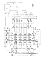
- the structure of a matrix M consists of m columns and n rows. At the intersection of column lines x1 to xm and row lines ys1 to ysn or yr1 to yrn, the matrix points consisting of an electromagnet R and two diodes Ds and Dr are connected. As shown in FIG. 1, one connection of the electromagnet R is connected to the assigned column line x1 to xm, while the other connection is connected via the one diode Ds to the assigned row setting line ys1 to ysn and via the other diode Dr to the assigned one Row reset line yr1 to yrn is connected. When setting, a set counter potential -Us is applied column by column.
- the row setting lines ys1 to ysn are applied synchronously and in pulses in succession with a setting potential + Us.
- the setting information is supplied by a processor P (not shown) to a column decoder Dx and a row decoder Dy.
- switches s1 and u1 only the thickly drawn circuit is effective in the control process shown in FIG. 1. Schematically specified contacts s1 to sn, r1 to rn and u1 to un pass on the addressing.
- the electromagnet designated with R is activated, which occurs via the addressing of the column decoder Dx and the row decoder Dy on the column line x1 with set counter potential -Us and via the row set line ys1, then only the optocoupler LEDs Osx1 and Osy1 respond when the Matrix has no errors.
- the output signals of these two optocoupler light-emitting diodes are fed to a code converter Dz via photo receivers of these optocouplers (not shown). Via the code converter Dz, these output signals are converted into binary information, which reaches a processor P on a reduced number z of information lines. This information can be easily compared in processor P with the pending set information. If a match is found, there is no error in the matrix M and no error signal is emitted.
- no optocoupler may respond to a control clock of a matrix point that is not to be set, whereas the optocoupler light-emitting diodes Osx1 and Osy1 connected to the assigned column line, for example x1, and the assigned row set line, for example ys1, must respond to a matrix point to be set. In this way, the controlled matrix points and therefore also the matrix M are checked with each control cycle.
- the optocoupler light-emitting diodes Osx1 to Osxm assigned to the column lines x1 to xm are combined with the optocoupler light-emitting diodes Orx1 to Orxm, which are also assigned to the column lines which are necessary for checking the matrix M during the reset process.
- These optocoupler light-emitting diodes Orx1 to Orxm are connected to the reset potential -Ur and respond when the reset counter potential is applied to the column lines x1 to xm + Ur is switched. As shown in FIG. 2, this is done in the column decoder Dx with schematically indicated addressing contacts u1 to um, which are controlled by the processor P.
- the optocoupler light-emitting diodes Ory1 to Oryn are also connected to the reset counter potential + Ur and respond when the assigned row reset line yr1 to yrn carries the reset potential -Ur.
- the electromagnet R When reset, the electromagnet R receives its current via the diode Dr, while when the electromagnet R is set, the current flows via the diode Ds. Setting and resetting is done by reversing the current. While the setting of the row setting lines ys1 to ysn in accordance with the desired setting depends on the position of the contacts s1 to sn when setting in the row decoder Dy, the column lines x1 to xm are acted upon by the setting counter potential -Us in each control cycle.
- the optocoupler light-emitting diodes Osy1 to Osyn and Ory1 to Oryn assigned to the line set lines ys1 to ysn and the line reset lines yr1 to yrn with the downstream photo receivers are also combined to form a unit Oy.
- the unit Ox has m set lines ms and m reset lines mr, while the unit Oy has n set outputs ns and n reset outputs nr corresponding to the number of lines. Checking in a control cycle is very simple because none of these outputs may carry a signal during the control pause.
- the line decoder Dy measures the current both when setting and when resetting.
- This current is monitored by current monitoring circuits SÜs and SÜr, it can be in a predetermined range, e.g. is given by the minimum and maximum current of a matrix point. Even if the current monitoring circuit SÜs or SÜr registers that the current range is below or exceeded during a set or reset cycle, an error signal is given, since then there is also an error in the matrix.
- the comparison information corresponding to the set or reset information is derived via the code converter Dz, so that the processor P can determine whether or not it matches - in the event of a mismatch, this can be done immediately or only after repeated detection of the mismatch Error signal are given.
- the current monitoring can also be carried out differently. It is thus possible to provide a common, central current monitoring circuit for the setting and resetting process, which is then accommodated in the central power supply part of the circuit arrangement.
- the reset can also be done so that a column line, e.g. x1, together with several row reset lines yr1 to yrn can be controlled.
- the control is again pulsed and synchronous.
- all of the matrix points connected to the driven row reset lines yr1 to yrn and leading to the driven column line x1 are reset.
- separate current monitoring circuits are then assigned to all line reset lines which are actuated at the same time. These current monitoring circuits can also be used several times if the matrix is divided into several such line blocks and is included in the control sequence of the processor.
Landscapes
- Engineering & Computer Science (AREA)
- Physics & Mathematics (AREA)
- General Physics & Mathematics (AREA)
- Theoretical Computer Science (AREA)
- Computer Hardware Design (AREA)
- Control Of Indicators Other Than Cathode Ray Tubes (AREA)
- Use Of Switch Circuits For Exchanges And Methods Of Control Of Multiplex Exchanges (AREA)
- Interface Circuits In Exchanges (AREA)
- Debugging And Monitoring (AREA)
- Electronic Switches (AREA)
- Devices For Indicating Variable Information By Combining Individual Elements (AREA)
- Tests Of Electronic Circuits (AREA)
- Monitoring And Testing Of Transmission In General (AREA)
Abstract
Description
- Die Erfindung betrifft eine Schaltungsanordnung für eine Anzeigevorrichtung mit einer aus n Zeilen und m Spalten bestehenden Matrix aus bistabilen Matrixpunkten, die jeweils einen Elektromagneten aufweisen, dessen einer Anschluß mit seiner zugeordneten Spaltenleitung und dessen anderer Anschluß stromrichtungsabhängig über entgegengesetzt gepolte Dioden mit seiner zugeordneten Zeilen-Setzleitung und seiner zugeordneten Zeilen-Rücksetzleitung verbunden sind, bei der die Spaltenleitungen, die Zeilen-Setzleitungen und die Zeilen-Rücksetzleitungen der Matrix über einen Prozessor, einen Spaltendekoder und einen Zeilen- dekoder beim Setzen oder Rücksetzen so ansteuerbar sind, daß die Spaltenleitungen zyklisch nacheinander mit Setzgegenpotential oder Rücksetzgegenpotential ansteuerbar sind, wobei bei jeder einzelnen Spaltenansteuerung zyklisch nacheinander alle Zeilen-Setzleitungen mit Setzpotential oder alle Zeilen-Rücksetzleitungen mit Rücksetzpotential ansteuerbar sind.
- Eine Schaltungsanordnung dieser Art ist aus B. Karpf: "Bistabile elektromagnetische Großanzeigen" in "Der Elektroniker" 7/84, Seiten 62 bis 65, bekannt. Diese bekannte Schaltungsanordnung dient lediglich zum Setzen und Rücksetzen der Matrixpunkte, eine Überwachung mit Überprüfung der einzelnen Matrixpunkte ist bei dieser bekannten Schaltungsanordnung nicht vorgesehen.
- Aus der Zeitschrift eee, Nummer 23 vom 18. Nov. 1986 ist auf den Seiten 32 und 34 eine Matrixansteuerung gezeigt, bei der die Ansteuersignale über Optokoppler auf die Zeilenleitungen der Matrix gegeben werden. Auch diese bekannte Matrixansteuerung weist keine Überwachung der Matrixpunkte auf.
- Es ist Aufgabe der Erfindung, eine Schaltungsanordnung der eingangs erwähnten Art zu schaffen, mit der beim Setzen und beim Rücksetzen der Matrixpunkte eine Überprüfung der Matrix auf Fehler vorgenommen wird, ohne daß dafür ein erheblicher Mehraufwand erforderlich ist.
- Diese Aufgabe wird nach der Erfindung dadurch gelöst, daß mit jeder Spaltenleitung eine an dem Setzpotential liegende erste Optokoppler-Leuchtdiode verbunden ist, die bei angelegtem Setzgegenpotential ein erstes Ausgangssignal abgibt, daß mit jeder Spaltenleitung eine an dem Rücksetzpotential liegende zweite Optokoppler-Leuchtdiode verbunden ist, die bei angelegtem Rücksetzgegenpotential ein zweites Ausgangssignal abgibt, daß mit jeder Zeilen-Setzleitung eine an dem Setzgegenpotential liegende dritte Optokoppler-Leuchtdiode verbunden ist, die bei angelegtem Setzpotential ein drittes Ausgangssignal abgibt, daß mit jeder Zeilen-Rücksetzleitung eine an dem Rücksetzgegenpotential liegende vierte Optokoppler-Leuchtdiode verbunden ist, die bei angelegtem Rücksetzpotential ein viertes Ausgangssignal abgibt, daß die Optokoppler-Leuchtdioden mittels zugeordneter Fotoempfänger Ausgangssignale einem Codewandler zuführen, der eine Vergleichsinformation an den Prozessor abgibt, und daß der Prozessor diese Vergleichsinformation auf Übereinstimmung mit der dem Spaltendekoder und dem Zeilendekoder zugeführten Setz- oder Rücksetzinformation überprüft und bei ein- oder mehrmaligem Fehlen der Übereinstimmung ein Fehlersignal abgibt.
- Mit Hilfe der an die Spaltenleitungen, die Zeilen-Setzleitungen und die Zeilen-Rücksetzleitungen angelegten Potentiale und angeschalteten Optokoppler kann bei jedem Setz- und Rücksetzvorgang ein Teil der Matrix überprüft werden. Es darf sowohl beim Setzen als auch beim Rücksetzen stets nur ein einziger Optokoppler ansprechen. Dies wird durch den zusätzlichen Codewandler überwacht, der nur bei ordnungsgemäß anstehender Ausgangsinformation der Optokoppler eine zugeordnete Information an den Prozessor abgibt. Dabei kann der Codewandler z.B. eine Binärinformation weiterleiten, um die Anzahl der Informationsleitungen zu reduzieren. Der Prozessor kann auf einfache Weise, z.B. über eine Tabelle, die vom Codewandler zugeführte Information mit der Setz- oder Rücksetzinformation vergleichen, die er gerade an den Spaltendekoder und den Zeilendekoder abgibt. Auf diese Weise wird bei jedem Setz-und Rücksetzvorgang der beteiligte Teil der Matrix überprüft.
- Um Kurzschlüsse und Unterbrechungen eines Matrixpunktes erfassen zu können, sieht eine Ausgestaltung vor, daß mittels Stromüberwachungsschaltungen beim Setzen und Rücksetzen ein vorgebbarer Strombereich überwacht ist. Der vorgebbare Strombereich ist dabei durch den Minimal-und Maximalstrom des Matrixpunktes vorgegeben und die Stromüberwachungsschaltungen sind im Zeilendekoder in die Leitungen zum Setz- und Rücksetzpotential eingeschleift.
- Für die Fehleranzeige ist nach einer weiteren Ausgestaltung vorgesehen, daß das Fehlersignal auch auftritt, wenn die Stromüberwachungsschaltungen ein Unter- oder Überschreiten des vorgebbaren Strombereiches feststellen.
- Das Setzen und Rücksetzen eines Matrixpunktes ist dabei vorzugsweise so, daß die Ansteuerung der Spaltenleitungen mit dem Setzgegenpotential bzw. dem Rücksetzgegenpotential und die Ansteuerung der Zeilen-Setzleitungen mit Setzpotential bzw. der Zeilen-Rücksetzleitungen mit Rücksetzpotential synchron und impulsförmig erfolgen.
- Der Strombereich eines Matrixpunktes läßt sich auch so überwachen, daß der Setz- und der Rücksetzstromkreis über eine gemeinsame Stromüberwachungsschaltung geführt ist, die im Stromversorgungs-Leistungsteil untergebracht ist.
- Der Rücksetzvorgang läßt sich nach einer Ausgestaltung dadurch verkürzen, daß beim Rücksetzen eine Spaltenleitung und gleichzeitig mehrere Zeilen-Rücksetzleitungen ansteuerbar sind und daß in jede Zeilen-Rücksetzleitung eine Stromüberwachungsschaltung eingeschleift ist.
- Der Aufbau der Matrix kann auch so sein, daß die Spalten und die Zeilen vertauschbar sind.
- Die Erfindung wird anhand eines in den Zeichnungen dargestellten Ausführungsbeispiels näher erläutert. Es zeigt:
- Fig. 1 schematisch eine Matrix mit Matrixpunkten und Prüfstromkreisen zum Feststellen von Fehlern in der Matrix, wobei der Matrixpunkt der Spalte 1 und der Zeile 1 gesetzt wird, und
- Fig. 2 denselben Matrixaufbau, wobei allerdings der Matrixpunkt der Spalte 1 und der Zeile 1 gerade zurückgesetzt wird.
- Der Aufbau einer Matrix M besteht aus m Spalten und n Zeilen. An den Kreuzungspunkten von Spaltenleitungen x1 bis xm und Zeilenleitungen ys1 bis ysn bzw. yr1 bis yrn sind die aus einem Elektromagneten R und aus zwei Dioden Ds und Dr bestehenden Matrixpunkte angeschaltet. Wie die Fig. 1 zeigt, ist der eine Anschluß des Elektromagneten R an die zugeordnete Spaltenleitung x1 bis xm angeschlossen, während der andere Anschluß über die eine Diode Ds an die zugeordnete Zeilen-Setzleitung ys1 bis ysn und über die andere Diode Dr an die zugeordnete Zeilen-Rücksetzleitung yr1 bis yrn angeschlossen ist. Beim Setzen wird Spalte um Spalte mit einem Setzgegenpotential -Us beaufschlagt. Bei jeder impulsförmigen Spaltenansteuerung werden die Zeilen-Setzleitungen ys1 bis ysn synchron und impulsförmig nacheinander mit einem Setzpotential + Us beaufschlagt. Die Setzinformation liefert ein nicht dargestellter Prozessor P an einen Spaltendekoder Dx und einen Zeilendekoder Dy. Wie mit Schaltern s1 und u1 angedeutet ist, wird bei dem in Fig. 1 gezeigten Steuervorgang nur der dick ausgezogene Stromkreis wirksam. Schematisch angegebene Kontakte s1 bis sn, r1 bis rn und u1 bis un geben die Adressierung weiter.
- Damit zusammen mit dem Setzvorgang die Matrix überprüft werden kann, ist an jede Spaltenleitung x1 bis xm eine auf das Setzgegenpotential -Us ansprechende Optokoppler-Leuchtdiode Osx1 bis Osxm angeschaltet. An die Zeilen-Setzleitungen ys1 bis ysn sind auf das Setzpotential ansprechende Optokoppler-Leuchtdioden Osy1 bis Osyn angeschaltet. Die Optokoppler-Leuchtdioden Osx1 bis Osxm der Spaltenleitungen x1 bis xm sind mit dem Setzpotential + Us und die Optokoppler-Leuchtdioden Osy1 bis Osyn der Zeilen-Setzleitungen ys1 bis ysn mit dem Setzgegenpotential -Us verbunden.
- Wird der mit R bezeichnete Elektromagnet angesteuert, der über die Adressierung des Spaltendekoders Dx und des Zeilendekoders Dy auf der Spaltenleitung x1 mit Setzgegenpotential -Us und über die Zeilen-Setzleitung ys1 erfolgt, dann sprechen nur die Optokoppler-Leuchtdioden Osx1 und Osy1 an, wenn die Matrix keinen Fehler aufweist. Die Ausgangssignale dieser beiden Optokoppler-Leuchtdioden werden über nicht dargestellte Fotoempfänger dieser Optokoppler einem Codewandler Dz zugeführt. Über den Codewandler Dz werden diese Ausgangssignale in eine binäre Information umgewandelt, die auf einer reduzierten Anzahl z von Informationsleitungen zu einem Prozessor P gelangt. Diese Information kann im Prozessor P auf einfache Weise mit der anstehenden Setzinformation verglichen werden. Wird dabei Übereinstimmung festgestellt, dann liegt in der Matrix M kein Fehler vor und es wird auch kein Fehlersignal abgegeben.
- Mit fortschreitendem Steuerzyklus werden der Reihe nach die übrigen Zeilen-Setzleitungen bis ysn angesteuert, wobei jedesmal die Spaltenleitung x1 impulsförmig mit angesteuert wird. Dann wiederholt sich dasselbe Spiel mit der Spaltenleitung x2 und wieder allen Zeilen-Setzleitungen ys1 bis ysn bis schließlich am Ende des Steuerzyklus die Spaltenleitung xm in den Unterzyklus mit den Zeilen-Setzleitungen ys1 bis ysn angesteuert wird. Auf diese Weise werden nacheinander alle Matrixpunkte angesteuert und gesetzt, wenn neben der angesteuerten Spaltenleitung x1 bis xm auch die angesteuerte Zeilen-Setzleitung ys1 bis ysn das richtige Potential erhält. Kontakte s1 können dabei entsprechend den zu setzenden Matrixpunkten vom Prozessor P ausgewählt und über den Zeilen- Dekoder Dy angesteuert werden. Bei einem Steuertakt eines nicht zu setzenden Matrixpunktes darf daher kein Optokoppler ansprechen, während bei einem zu setzenden Matrixpunkt die mit der zugeordneten Spaltenleitung, z.B. x1, und der zugeordneten Zeilen-Setzleitung, z.B. ys1, verbundenen Optokoppler-Leuchtdioden Osx1 und Osy1 ansprechen müssen. Auf diese Weise erfolgt mit jedem Steuertakt eine Überprüfung der angesteuerten Matrixpunkte und daher auch der Matrix M. Die den Spaltenleitungen x1 bis xm zugeordneten Optokoppler-Leuchtdioden Osx1 bis Osxm werden mit den ebenfalls den Spaltenleitungen zugeordneten Optokoppler-Leuchtdioden Orx1 bis Orxm zu einer Baueinheit Ox zusammengefaßt, die für die Überprüfung der Matrix M beim Rücksetzvorgang erforderlich sind. Diese Optokoppler-Leuchtdioden Orx1 bis Orxm sind mit dem Rücksetzpotential -Ur verbunden und sprechen an, wenn auf die Spaltenleitungen x1 bis xm das Rücksetzgegenpotential + Ur geschaltet wird. Wie die Fig. 2 zeigt, erfolgt dies im Spaltendekoder Dx mit schematisch angedeuteten Adressierungskontakten u1 bis um, die vom Prozessor P gesteuert werden.
- Außerdem sind an die Zeilen-Rücksetzleitungen yr1 bis yrn die Optokoppler-Leuchtdioden Ory1 bis Oryn angeschaltet, die mit dem Rücksetzgegenpotential + Ur verbunden sind und ansprechen, wenn die zugeordnete Zeilen-Rücksetzleitung yr1 bis yrn das Rücksetzpotential -Ur führt.
- Beim Rücksetzen erhält der Elektromagnet R über die Diode Dr seinen Strom, während beim Setzen des Elektromagneten R der Strom über die Diode Ds fließt. Setzen und Rücksetzen erfolgt also durch Stromumkehr. Während beim Setzen im Zeilen-Dekoder Dy die Ansteuerung der Zeilen-Setzleitungen ys1 bis ysn entsprechend der gewünschten Einstellung abhängig von der Stellung der Kontakte s1 bis sn ist, werden die Spaltenleitungen x1 bis xm in jedem Steuertakt mit dem Setzgegenpotential -Us beaufschlagt. Beim Rücksetzen werden dagegen alle Zeilen-Rücksetzleitungen yr1 bis yrn in den zugeordneten Steuertakten mit dem Rücksetzpotential -Ur beaufschlagt, während den Spaltenleitungen x1 bis xm in den Steuertakten das Rücksetzgegenpotential + Ur zugeführt wird. Auf diese Weise werden auch beim Steuerzyklus des Rücksetzens die Matrixpunkte und damit die Matrix M auf Fehler überprüft.
- Auch die den Zeilen-Setzleitungen ys1 bis ysn und den Zeilen-Rücksetzleitungen yr1 bis yrn zugeordneten Optokoppler-Leuchtdioden Osy1 bis Osyn und Ory1 bis Oryn mit den nachgeschalteten Fotoempfängern werden zu einer Einheit Oy zusammengefaßt. Die Einheit Ox hat m Setzleitungen ms und m Rücksetzleitungen mr, während die Einheit Oy entsprechend der Zeilenzahl n Setzausgänge ns und n Rücksetzausgänge nr hat. Die Überprüfung in einem Steuertakt ist sehr einfach, denn in der Steuerpause darf keiner dieser Ausgänge ein Signal führen. Bei einem Setztakt darf nur ein einziger Setzausgang ms und ein einziger Setzausgang ns ein Ausgangssignal führen, während bei einem Rücksetztakt nur ein einziger Rücksetzausgang mr und ein einziger Rücksetzausgang nr ein Ausgangssignal führen darf. Dabei müssen aber beim Setz- und beim Rücksetztakt diese beiden Ausgangssignale auch gleichzeitig anwesend sein. Fehlt ein Ausgangssignal, dann liegt an dem angesteuerten Matrixpunkt ein Fehler vor.
- Um die Überprüfung noch weiterzuführen, wird im Zeilendekoder Dy sowohl beim Setzen als auch beim Rücksetzen der Strom gemessen. Dieser Strom wird durch Stromüberwachungsschaltungen SÜs und SÜr überwacht, er kann in einem vorgegebenen Bereich liegen, der z.B. durch den Minimal-und Maximalstrom eines Matrixpunktes gegeben ist. Auch wenn während eines Setz- oder Rücksetztaktes die Stromüberwachungsschaltung SÜs oder SÜr ein Unter- oder Überschreiten dieses Strombereiches registriert, wird ein Fehlersignal gegeben, da dann ebenfalls ein Fehler in der Matrix vorliegt.
- In jedem Setztakt und in jedem Rücksetztakt wird über den Codewandler Dz die der Setz- oder Rücksetzinformation entsprechende Vergleichsinformation abgeleitet, so daß im Prozessor P die Übereinstimmung oder Nichtübereinstimmung mit dieser festgestellt werden kann - Bei Nichtübereinstimmung kann sofort oder auch erst bei mehrmaligem Feststellen der Nichtübereinstimmung das Fehlersignal gegeben werden.
- Die Stromüberwachung kann auch anders ausgeführt sein. So ist es möglich, für den Setz- und Rücksetzvorgang eine gemeinsame, zentrale Stromüberwachungsschaltung vorzusehen, die dann im zentralen Stromversorgungsteil der Schaltungsanordnung untergebracht ist.
- Das Rücksetzen kann auch so erfolgen, daß eine Spaltenleitung, z.B. x1, zusammen mit mehreren Zeilen-Rücksetzleitungen yr1 bis yrn ansteuerbar ist. Die Ansteuerung erfolgt dabei wieder impulsförmig und synchron. Es werden aber alle an den angesteuerten Zeilen-Rücksetzleitungen yr1 bis yrn angeschalteten und zu der angesteuerten Spaltenleitung x1 führenden Matrixpunkte zurückgesetzt. Für die Stromüberwachung werden dann allen gleichzeitig angesteuerten Zeilen-Rücksetzleitungen getrennte Stromüberwachungsschaltungen zugeordnet. Auch diese Stromüberwachungsschaltungen können mehrfach ausgenützt werden, wenn die Matrix in mehrere solche Zeilenblöcke unterteilt in den Steuerungsablauf des Prozessors einbezogen ist.
Claims (9)
dadurch gekennzeichnet,
Applications Claiming Priority (2)
| Application Number | Priority Date | Filing Date | Title |
|---|---|---|---|
| DE4024499A DE4024499C1 (de) | 1990-08-02 | 1990-08-02 | |
| DE4024499 | 1990-08-02 |
Publications (3)
| Publication Number | Publication Date |
|---|---|
| EP0471935A2 true EP0471935A2 (de) | 1992-02-26 |
| EP0471935A3 EP0471935A3 (en) | 1992-06-17 |
| EP0471935B1 EP0471935B1 (de) | 1994-09-14 |
Family
ID=6411481
Family Applications (1)
| Application Number | Title | Priority Date | Filing Date |
|---|---|---|---|
| EP91109646A Expired - Lifetime EP0471935B1 (de) | 1990-08-02 | 1991-06-12 | Schaltungsanordnung zum Überwachen einer Matrix aus bistabilen Matrixpunkten |
Country Status (5)
| Country | Link |
|---|---|
| US (1) | US5301200A (de) |
| EP (1) | EP0471935B1 (de) |
| AT (1) | ATE111624T1 (de) |
| CA (1) | CA2047911C (de) |
| DE (2) | DE4024499C1 (de) |
Families Citing this family (4)
| Publication number | Priority date | Publication date | Assignee | Title |
|---|---|---|---|---|
| DE4212125C1 (de) * | 1992-04-13 | 1993-04-01 | Dambach-Werke Gmbh, 7554 Kuppenheim, De | |
| DE4236117C1 (de) * | 1992-07-16 | 1993-10-07 | Gassmann Gerhard G | Matrixförmige Anzeigevorrichtung |
| DE19640120A1 (de) * | 1996-09-28 | 1998-04-02 | Pks Systemtechnik | Schaltungsanordnung und Verfahren zur Überprüfung einer Schaltungs-Matrix |
| DE19710855A1 (de) * | 1997-03-15 | 1998-10-01 | Dambach Werke Gmbh | Leuchtdiodenmatrix-Anzeigevorrichtung |
Family Cites Families (4)
| Publication number | Priority date | Publication date | Assignee | Title |
|---|---|---|---|---|
| US4069480A (en) * | 1977-01-03 | 1978-01-17 | Ferranti-Packard Limited | Blanking circuit for electromagnetic display |
| US4263647A (en) * | 1979-02-07 | 1981-04-21 | Allen-Bradley Company | Fault monitor for numerical control system |
| FR2566565B1 (fr) * | 1984-06-25 | 1986-11-28 | Dev Prod Elect Et | Dispositif d'affichage comportant des elements unitaires a commande electrique commandes par un reseau matriciel a diodes |
| US4675575A (en) * | 1984-07-13 | 1987-06-23 | E & G Enterprises | Light-emitting diode assemblies and systems therefore |
-
1990
- 1990-08-02 DE DE4024499A patent/DE4024499C1/de not_active Expired - Fee Related
-
1991
- 1991-06-12 EP EP91109646A patent/EP0471935B1/de not_active Expired - Lifetime
- 1991-06-12 AT AT91109646T patent/ATE111624T1/de not_active IP Right Cessation
- 1991-06-12 DE DE59102919T patent/DE59102919D1/de not_active Expired - Fee Related
- 1991-07-25 CA CA002047911A patent/CA2047911C/en not_active Expired - Fee Related
- 1991-08-01 US US07/738,507 patent/US5301200A/en not_active Expired - Fee Related
Also Published As
| Publication number | Publication date |
|---|---|
| DE59102919D1 (de) | 1994-10-20 |
| ATE111624T1 (de) | 1994-09-15 |
| CA2047911C (en) | 1996-01-16 |
| DE4024499C1 (de) | 1991-09-26 |
| US5301200A (en) | 1994-04-05 |
| CA2047911A1 (en) | 1992-02-03 |
| EP0471935A3 (en) | 1992-06-17 |
| EP0471935B1 (de) | 1994-09-14 |
Similar Documents
| Publication | Publication Date | Title |
|---|---|---|
| DE1437824B2 (de) | Einrichtung zur Synchronisierung von Impulsgeneratoren | |
| DE69231311T2 (de) | Optoelektronische Schranke | |
| EP0371317B1 (de) | Lichtschranken-Sicherheitseinrichtung | |
| EP0471935B1 (de) | Schaltungsanordnung zum Überwachen einer Matrix aus bistabilen Matrixpunkten | |
| DE2853546A1 (de) | Pruefschaltung fuer synchron arbeitende taktgeber | |
| EP0207284A2 (de) | Verfahren zur Synchronisierung von Rechtecksignalen | |
| DE69320421T2 (de) | Steuereinrichtung für einen Thyristorumrichter | |
| DE1524513C3 (de) | Anzeigevorrichtung | |
| EP0579912A2 (de) | Überwachungseinrichtung für mehrere elektrische Schalter | |
| EP0037965A2 (de) | Einrichtung zum Prüfen einer digitalen Schaltung mittels in diese Schaltung eingebauter Prüfschaltungen | |
| DE1295627B (de) | Schaltungsanordnung zur UEberwachung von Taktgebern | |
| DE1812529A1 (de) | Operatorkonsol mit Kathodenstrahlroehre | |
| DE69400786T2 (de) | Verfahren und Vorrichtung zum Überwachen von Signalen von Wandlern und optischen Encodern | |
| DE1259230B (de) | Einrichtung zur Fernueberwachung | |
| DE1954910C3 (de) | Anordnung zur Anzeige eines Defekts von Entkopplungsdioden in einer Matrix | |
| DE1044897B (de) | Pruefschaltung zur Mehrdeutigkeits- und Vollstaendigkeitspruefung | |
| DE2165308A1 (de) | Einrichtung für eine Signalis&tions- und Meldeanlage | |
| DE1762173B2 (de) | Kodegenerator | |
| DE3012045A1 (de) | Anordnung und verfahren zum ein- und ausschalten von verbrauchern mit einem mikroprozessor | |
| DE1774218C (de) | Mechanisches Zählwerk mit Impulsgeber | |
| DE2447106C2 (de) | Schaltungsanordnung zur Ansteuerung von Meldelampen und einer Hupe | |
| DE1791062C3 (de) | Anordnung zur Anzeige von Meldezuständen bei zyklischer Abfrage | |
| DE1287131B (de) | Elektronische Impulszaehleranordnung zur Anzeige der Verschiebung eines beweglichen Teils bezueglich einer vorgegebenen Stellung | |
| EP0448134A2 (de) | Einrichtung zum optischen Überwachen eines Geschehens auf einer Meldetafel | |
| DE1499262C (de) | Einrichtung zur Auswahl der richtigen von zwei parallel betriebenen Datenverarbei tungsanlagen |
Legal Events
| Date | Code | Title | Description |
|---|---|---|---|
| PUAI | Public reference made under article 153(3) epc to a published international application that has entered the european phase |
Free format text: ORIGINAL CODE: 0009012 |
|
| AK | Designated contracting states |
Kind code of ref document: A2 Designated state(s): AT BE CH DE DK ES FR GB GR IT LI LU NL SE |
|
| PUAL | Search report despatched |
Free format text: ORIGINAL CODE: 0009013 |
|
| AK | Designated contracting states |
Kind code of ref document: A3 Designated state(s): AT BE CH DE DK ES FR GB GR IT LI LU NL SE |
|
| 17P | Request for examination filed |
Effective date: 19920602 |
|
| 17Q | First examination report despatched |
Effective date: 19931206 |
|
| ITF | It: translation for a ep patent filed | ||
| GRAA | (expected) grant |
Free format text: ORIGINAL CODE: 0009210 |
|
| AK | Designated contracting states |
Kind code of ref document: B1 Designated state(s): AT BE CH DE DK ES FR GB GR IT LI LU NL SE |
|
| PG25 | Lapsed in a contracting state [announced via postgrant information from national office to epo] |
Ref country code: GR Free format text: LAPSE BECAUSE OF FAILURE TO SUBMIT A TRANSLATION OF THE DESCRIPTION OR TO PAY THE FEE WITHIN THE PRESCRIBED TIME-LIMIT Effective date: 19940914 Ref country code: ES Free format text: THE PATENT HAS BEEN ANNULLED BY A DECISION OF A NATIONAL AUTHORITY Effective date: 19940914 Ref country code: DK Effective date: 19940914 |
|
| REF | Corresponds to: |
Ref document number: 111624 Country of ref document: AT Date of ref document: 19940915 Kind code of ref document: T |
|
| REF | Corresponds to: |
Ref document number: 59102919 Country of ref document: DE Date of ref document: 19941020 |
|
| ET | Fr: translation filed | ||
| PG25 | Lapsed in a contracting state [announced via postgrant information from national office to epo] |
Ref country code: SE Effective date: 19941214 |
|
| GBT | Gb: translation of ep patent filed (gb section 77(6)(a)/1977) |
Effective date: 19941219 |
|
| PG25 | Lapsed in a contracting state [announced via postgrant information from national office to epo] |
Ref country code: LU Free format text: LAPSE BECAUSE OF NON-PAYMENT OF DUE FEES Effective date: 19950630 |
|
| PLBE | No opposition filed within time limit |
Free format text: ORIGINAL CODE: 0009261 |
|
| STAA | Information on the status of an ep patent application or granted ep patent |
Free format text: STATUS: NO OPPOSITION FILED WITHIN TIME LIMIT |
|
| 26N | No opposition filed | ||
| PGFP | Annual fee paid to national office [announced via postgrant information from national office to epo] |
Ref country code: BE Payment date: 19990806 Year of fee payment: 9 |
|
| PG25 | Lapsed in a contracting state [announced via postgrant information from national office to epo] |
Ref country code: BE Free format text: LAPSE BECAUSE OF NON-PAYMENT OF DUE FEES Effective date: 20000630 |
|
| PGFP | Annual fee paid to national office [announced via postgrant information from national office to epo] |
Ref country code: FR Payment date: 20000630 Year of fee payment: 10 |
|
| BERE | Be: lapsed |
Owner name: DAMBACH-WERKE G.M.B.H. Effective date: 20000630 |
|
| REG | Reference to a national code |
Ref country code: GB Ref legal event code: IF02 |
|
| PG25 | Lapsed in a contracting state [announced via postgrant information from national office to epo] |
Ref country code: FR Free format text: LAPSE BECAUSE OF NON-PAYMENT OF DUE FEES Effective date: 20020228 |
|
| PGFP | Annual fee paid to national office [announced via postgrant information from national office to epo] |
Ref country code: NL Payment date: 20020628 Year of fee payment: 12 |
|
| PGFP | Annual fee paid to national office [announced via postgrant information from national office to epo] |
Ref country code: GB Payment date: 20030523 Year of fee payment: 13 |
|
| PGFP | Annual fee paid to national office [announced via postgrant information from national office to epo] |
Ref country code: DE Payment date: 20030526 Year of fee payment: 13 Ref country code: CH Payment date: 20030526 Year of fee payment: 13 |
|
| PGFP | Annual fee paid to national office [announced via postgrant information from national office to epo] |
Ref country code: AT Payment date: 20030528 Year of fee payment: 13 |
|
| PG25 | Lapsed in a contracting state [announced via postgrant information from national office to epo] |
Ref country code: NL Free format text: LAPSE BECAUSE OF NON-PAYMENT OF DUE FEES Effective date: 20040101 |
|
| NLV4 | Nl: lapsed or anulled due to non-payment of the annual fee |
Effective date: 20040101 |
|
| PG25 | Lapsed in a contracting state [announced via postgrant information from national office to epo] |
Ref country code: GB Free format text: LAPSE BECAUSE OF NON-PAYMENT OF DUE FEES Effective date: 20040612 Ref country code: AT Free format text: LAPSE BECAUSE OF NON-PAYMENT OF DUE FEES Effective date: 20040612 |
|
| PG25 | Lapsed in a contracting state [announced via postgrant information from national office to epo] |
Ref country code: LI Free format text: LAPSE BECAUSE OF NON-PAYMENT OF DUE FEES Effective date: 20040630 Ref country code: CH Free format text: LAPSE BECAUSE OF NON-PAYMENT OF DUE FEES Effective date: 20040630 |
|
| PG25 | Lapsed in a contracting state [announced via postgrant information from national office to epo] |
Ref country code: DE Free format text: LAPSE BECAUSE OF NON-PAYMENT OF DUE FEES Effective date: 20050101 |
|
| GBPC | Gb: european patent ceased through non-payment of renewal fee |
Effective date: 20040612 |
|
| REG | Reference to a national code |
Ref country code: CH Ref legal event code: PL |
|
| PG25 | Lapsed in a contracting state [announced via postgrant information from national office to epo] |
Ref country code: IT Free format text: LAPSE BECAUSE OF NON-PAYMENT OF DUE FEES;WARNING: LAPSES OF ITALIAN PATENTS WITH EFFECTIVE DATE BEFORE 2007 MAY HAVE OCCURRED AT ANY TIME BEFORE 2007. THE CORRECT EFFECTIVE DATE MAY BE DIFFERENT FROM THE ONE RECORDED. Effective date: 20050612 |