EP0467667A2 - Circuit d'alimentation pour appareillages électroniques - Google Patents
Circuit d'alimentation pour appareillages électroniques Download PDFInfo
- Publication number
- EP0467667A2 EP0467667A2 EP91306503A EP91306503A EP0467667A2 EP 0467667 A2 EP0467667 A2 EP 0467667A2 EP 91306503 A EP91306503 A EP 91306503A EP 91306503 A EP91306503 A EP 91306503A EP 0467667 A2 EP0467667 A2 EP 0467667A2
- Authority
- EP
- European Patent Office
- Prior art keywords
- voltage
- boosting circuit
- electronic equipment
- power supply
- circuit
- Prior art date
- Legal status (The legal status is an assumption and is not a legal conclusion. Google has not performed a legal analysis and makes no representation as to the accuracy of the status listed.)
- Granted
Links
Images

Classifications
-
- H—ELECTRICITY
- H02—GENERATION; CONVERSION OR DISTRIBUTION OF ELECTRIC POWER
- H02M—APPARATUS FOR CONVERSION BETWEEN AC AND AC, BETWEEN AC AND DC, OR BETWEEN DC AND DC, AND FOR USE WITH MAINS OR SIMILAR POWER SUPPLY SYSTEMS; CONVERSION OF DC OR AC INPUT POWER INTO SURGE OUTPUT POWER; CONTROL OR REGULATION THEREOF
- H02M3/00—Conversion of dc power input into dc power output
- H02M3/02—Conversion of dc power input into dc power output without intermediate conversion into ac
- H02M3/04—Conversion of dc power input into dc power output without intermediate conversion into ac by static converters
- H02M3/06—Conversion of dc power input into dc power output without intermediate conversion into ac by static converters using resistors or capacitors, e.g. potential divider
- H02M3/07—Conversion of dc power input into dc power output without intermediate conversion into ac by static converters using resistors or capacitors, e.g. potential divider using capacitors charged and discharged alternately by semiconductor devices with control electrode, e.g. charge pumps
-
- G—PHYSICS
- G04—HOROLOGY
- G04C—ELECTROMECHANICAL CLOCKS OR WATCHES
- G04C10/00—Arrangements of electric power supplies in time pieces
Definitions
- This invention relates to a power supply circuit for electronic equipment, and especially to a circuit for controlling the power supply for such equipment.
- a secondary power source such as a high capacitance condenser (referred to as a capacitor hereinafter), stores the generated electric energy.
- the voltage from the secondary power source is stepped up by a boosting circuit to provide a main supply voltage.
- the capacitor voltage is designated as a primary voltage and the output voltage from the boosting circuit is designated as a secondary voltage
- the secondary voltage is used to generate control signals for the operation of the boosting circuit.
- such an arrangement has various technical problems resulting from the use of switching transistors in the boosting circuit.
- Id ⁇ (V GS - V TH)2/2
- Id ⁇ ⁇ (V GS - V TH) V DS - 2 V DS2 ⁇ /2
- V GS the potential difference between the gate and the source
- V TH the threshold voltage
- V DS the potential difference between the drain and the source of the transistor
- ⁇ W/L ⁇ n C ox
- W is the channel width
- L is the channel length
- ⁇ n is the surface migration of electrons
- C ox is the capacitance of the gate oxide film.
- V GS becomes less than V TH in the above equations so that the relevant transistor fails to conduct, terminating the voltage boosting operation.
- Such a shutdown of the power supply is detrimental to the electronic equipment, which employs a capacitor charged by the boosted voltage as the main source of power. As a result, the electronic equipment itself may shut down entirely.
- a power supply circuit for electronic equipment comprising power generating means, a secondary power source for storing an output from the power generating means for supplying a primary voltage (Vsc), and a boosting circuit for stepping the primary voltage up to a secondary voltage (Vss1) for supply to the electronic equipment, and characterised by means for generating control signals (P) at a voltage level (Vss2) higher than that of the secondary voltage for controlling operation of the boosting circuit.
- the present invention offers reliable operation of the boosting circuit, even when the capacitor voltage reaches a certain voltage level or when the boosted voltage is low, and hence reduces or avoids the likelihood of the electronic equipment shutting down.
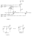
- Figure 1 is a schematic diagram of a power supply circuit according to the present invention having a power generating device and being incorporated in an electronic wristwatch.
- a power generator coil 1 generates an AC voltage, employing a generating device such as the one described in Japanese Published Patent Application No. 61-093978.
- a rectifier diode 2 provides half wave rectification of the AC voltage and supplies the rectified voltage to a high capacitance capacitor 3 to charge the same.
- a limiter 4, serving as a switching device for preventing overcharging of the capacitor 3, is activated at a moment when the voltage V SC at the capacitor 3 reaches a pre-determined voltage level, the limiter 4 then serving as a by-pass for the output from the generator coil 1.
- a first boosting circuit 5 steps up the voltage V SC for supply to an auxiliary capacitor 6 for charging the same.
- a control circuit 7 of the wristwatch is driven by the voltage Vss1 at the auxiliary capacitor 6, the voltage Vss1 being the main source of supply for the wristwatch.
- the wristwatch further comprises a crystal oscillator 8 serving as the source of a time standard and oscillating at a frequency of 32768Hz; and a coil 9 of a known stepping motor linked to the wristwatch hands to show the time.
- a second boosting circuit 10 further steps up the main supply voltage Vss1 to a voltage Vss2 using a known charging technique with a capacitor.
- the voltage Vss2 output by the second boosting circuit 10 is supplied to a level converter 11, in the form of a known voltage detector, which also receives an input control signal P′ at a voltage level corresponding with the voltage Vss1 from the control circuit 7 and converts the signal P′ into a control signal P whose voltage level corresponds with the voltage Vss2.
- the converted control signal P is then supplied by the level converter 11 to the first boosting circuit 5.
- a control signal N directly from the control circuit 7, whose voltage level corresponds with the voltage Vss1 with no conversion, is also supplied to the first boosting circuit 5.
- An immediate start resistor 12 activates oscillation at the start of operation of the wristwatch using the voltage drop thereacross generated by the AC voltage.
- a voltage detector 14 controls the on/off operation of both the transistor 13 and the limiter 4, by comparing the voltage V SC of the capacitor 3 with pre-determined voltage thresholds V ON and V LIM at two levels. When V SC ⁇ V ON, it is assumed that the operation of the wristwatch is being started and the transistor 13 is switched off. The immediate start resistor 12 is thus rendered effective. When V SC > V ON, it is assumed that a sufficiently high operating voltage has been reached and the transistor 13 is switched on.
- the voltage threshold V LIM is pre-set to a level near the maximum voltage rating of the capacitor 3 so that, at the moment when V SC becomes greater than V LIM, the limiter 4 is activated to protect the capacitor 3 against overcharging.
- FIG 2 is a schematic diagram of the first boosting circuit 5.
- a capacitor 15 is used to store the charge in the auxiliary capacitor 3.
- the charging of the capacitor 15 is effected by alternating between two different connections through an arrangement of MOSFETs 16 to 19, at a timing determined by the input control signals N and P.
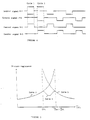
- Figure 3 is a functional drawing of the two connections. This is a known charging technique, by which the voltage Vss1 of the auxiliary capacitor 6 becomes twice the voltage V SC of the capacitor 3.
- Figure 4 is a timing chart showing the control signals P-1, P-2, N-1 and N-2 supplied to the circuit 5 for control of the on/off operation of the MOSFETs 16 to 19 shown in figure 2 and hence of the charging cycle of the capacitor 15.
- both the control signals P-1 and N-1 are in an active state, causing the MOSFETs 16 and 18 to be on.
- both the control signals P-2 and N-2 are in an active state, causing the MOSFETs 17 and 19 to be on. This switching allows the two connections to alternate.
- both the control signals P-1 and P-2 are supplied directly from the control circuit 7 without conversion from the level of the voltage Vss1 to the level of the voltage Vss2.
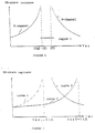
- the horizontal axis represents the voltage V SC of the capacitor 3, and the vertical axis represents the on state resistance of the MOSFET 18.
- the MOSFET 18 employs complimentary P channel and N channel MOSFET devices with the N channel device conducting in the high voltage range of V SC and the P channel device conducting in the low voltage range of V SC. More specifically, the gate voltage in the N channel device becomes a ground voltage V DD in response to the control signal N-1 during cycle 1, the source voltage becomes V SC and the voltage difference V GS between the gate voltage and the source voltage also becomes equal to V SC. Now if V GS, and therefore V SC, is greater than the threshold voltage V TH of the N channel MOSFET device, the N channel device is switched on and current Id flows as equation 1 above suggests. Curve 1 in figure 5 represents the on state resistance characteristic of the N channel MOSFET device, indicating that this device is switched on in the region where V SC > V TH.
- the gate voltage in the P channel device becomes the voltage Vss1 in response to the control signal P-1 during cycle 1, the source voltage is V SC and the voltage difference V GS becomes (Vss1 - V SC).
- V GS and therefore (Vss1 - V SC)
- V TH threshold voltage of the P channel MOSFET device
- Curve 2 in figure 5 represents the on-state resistance of the P channel MOSFET device indicating that this is switched on in the region where (Vss1 - V SC) > V TH, in other words where V SC ⁇ (Vss1 - V TH).
- Curve 3 in figure 5 represents a composite on-state resistance of the P channel MOSFET device and the N channel MOSFET device. This curve shows that the first boosting circuit 5 functions over the entire range of V SC without the on-state resistance increasing to infinity.
- Figure 6 illustrates an example of such a situation wherein a high threshold voltage V TH occurs and the current Id cannot flow in a region 1 in which the on-state resistance increases to infinity.
- the value (V SC - V TH) for the N channel MOSFET device is negative
- the value (Vss1 - V SC - V TH) for the P channel MOSFET device is negative as well. This means that the two devices are unable to compensate for each other.
- V SC and Vss1 become lower gradually and, when the voltage Vss1 happens to fall instantaneously, because of motor drive pulse output for example, the value (Vss1 - V SC - V TH) changes from positive to negative again causing the region 1 to be generated and leading to the shutdown of the boosting operation.
- the second boosting circuit 10 and the level converter 11 are provided for converting both the control signals P-1 and P-2 serving as gate control signals for the P channel MOSFET device to the level of the voltage Vss2.
- the voltage V GS for the P channel MOSFET device thus becomes (Vss2 - V SC).
- the value (Vss2 - V SC - V TH), in equation 1, can be kept positive, because the voltage Vss2 increases and reaches a voltage level twice that of the voltage Vss1 through the second boosting circuit 10 in figure 1.
- FIG. 7 illustrates this.
- Dashed curve 1 in figure 7 represents the conventional case where the P channel MOSFET device is controlled by the voltage Vss1. It should be noted that the on-state resistance then increases to infinity at the threshold line representing the value (Vss1 - V TH).
- curve 2 in figure 7 represents the case in the present invention where switching is controlled by the voltage Vss2. It should be noted that since the threshold line is shifted to a higher voltage at the value (Vss2 - V TH), the composite resistance, including the resistance of the N channel MOSFET device (curve 3), is kept from increasing to infinity.
- the voltage V GS becomes (Vss2 - V TH) when the gate control signal P-2 for the P channel MOSFET device is converted to the level of the voltage Vss2 and the voltage V GS for the N channel MOSFET device becomes V TH.
- the present invention thus provides the same improvement for the MOSFET 17 as in the case of the MOSFET 18.
- the threshold voltage of the P channel MOSFET device of the boosting circuit is shifted from (Vss1 - V TH) to (Vss2 - V TH), greater tolerance in the specification requirements for the voltage V TH in the IC manufacturing process becomes possible. Consequently, a higher yield rate is possible in the production of the ICs together with a reduction in cost.
Landscapes
- Engineering & Computer Science (AREA)
- Power Engineering (AREA)
- Physics & Mathematics (AREA)
- General Physics & Mathematics (AREA)
- Dc-Dc Converters (AREA)
- Electromechanical Clocks (AREA)
- Control Of Charge By Means Of Generators (AREA)
Applications Claiming Priority (3)
| Application Number | Priority Date | Filing Date | Title |
|---|---|---|---|
| JP2189690A JP3000633B2 (ja) | 1990-07-18 | 1990-07-18 | 電子機器 |
| JP18969090 | 1990-07-18 | ||
| JP189690/90 | 1990-07-18 |
Publications (4)
| Publication Number | Publication Date |
|---|---|
| EP0467667A2 true EP0467667A2 (fr) | 1992-01-22 |
| EP0467667A3 EP0467667A3 (en) | 1992-04-15 |
| EP0467667B1 EP0467667B1 (fr) | 1995-09-27 |
| EP0467667B2 EP0467667B2 (fr) | 2001-07-25 |
Family
ID=16245556
Family Applications (1)
| Application Number | Title | Priority Date | Filing Date |
|---|---|---|---|
| EP91306503A Expired - Lifetime EP0467667B2 (fr) | 1990-07-18 | 1991-07-17 | Circuit d'alimentation pour appareillages électroniques |
Country Status (7)
| Country | Link |
|---|---|
| US (1) | US5130960A (fr) |
| EP (1) | EP0467667B2 (fr) |
| JP (1) | JP3000633B2 (fr) |
| KR (1) | KR960005689B1 (fr) |
| CN (1) | CN1033539C (fr) |
| DE (1) | DE69113347T3 (fr) |
| HK (1) | HK1007219A1 (fr) |
Cited By (2)
| Publication number | Priority date | Publication date | Assignee | Title |
|---|---|---|---|---|
| EP0695978A1 (fr) | 1994-08-03 | 1996-02-07 | Seiko Instruments Inc. | Montre de contrÔle électronique |
| EP0695980A1 (fr) * | 1994-02-23 | 1996-02-07 | Citizen Watch Co. Ltd. | Excitateur courant continu |
Families Citing this family (14)
| Publication number | Priority date | Publication date | Assignee | Title |
|---|---|---|---|---|
| JPH0996686A (ja) * | 1995-09-29 | 1997-04-08 | Citizen Watch Co Ltd | 電子時計とその充電方法 |
| DK0848842T3 (da) * | 1996-06-26 | 1999-11-08 | Konrad Schafroth | Urværk |
| JP3624665B2 (ja) * | 1997-02-07 | 2005-03-02 | セイコーエプソン株式会社 | 発電装置、充電方法および計時装置 |
| DE69941484D1 (de) * | 1999-01-06 | 2009-11-12 | Seiko Epson Corp | Elektronische vorrichtung und verfahren um die elektrosnische vorrichtung anzusteuern |
| KR20030083374A (ko) * | 2002-04-22 | 2003-10-30 | 유지고하라 | 직류전류의 불변동분할을 가능하도록한 에너지 절약장치 |
| CN100535801C (zh) * | 2002-09-19 | 2009-09-02 | 西铁城控股株式会社 | 电子时钟 |
| DE602005013452D1 (de) * | 2004-02-26 | 2009-05-07 | Seiko Epson Corp | Steuerungseinrichtung, elektronischer apparat, ste steuerungsprogramm für eine elektronischen apparat, aufzeichnungsmedium |
| US20060114750A1 (en) * | 2004-11-29 | 2006-06-01 | Seiko Epson Corporation | Electronic apparatus, method for detecting positions of time display members in electronic apparatus, and program for detecting positions of time display members in electronic apparatus |
| JP4753826B2 (ja) * | 2006-09-28 | 2011-08-24 | パナソニック株式会社 | 多出力電源装置 |
| EP2218586B1 (fr) * | 2007-11-26 | 2014-03-12 | Mitsubishi Pencil Company, Limited | Crayon mécanique |
| JP2010233380A (ja) * | 2009-03-27 | 2010-10-14 | Seiko Epson Corp | 電源供給回路及び電子デバイス |
| US11205382B2 (en) | 2018-11-22 | 2021-12-21 | Novatek Microelectronics Corp. | Sensing circuit for OLED driver and OLED driver using the same |
| CN111471002B (zh) | 2020-04-22 | 2022-08-09 | 潜江永安药业股份有限公司 | 一种制备高纯度牛磺酸和盐的方法和系统 |
| KR102680775B1 (ko) * | 2021-11-29 | 2024-07-02 | 심정석 | 친환경 세정액 용기의 제조방법 |
Citations (5)
| Publication number | Priority date | Publication date | Assignee | Title |
|---|---|---|---|---|
| US4060974A (en) * | 1975-07-02 | 1977-12-06 | Citizen Watch Company Limited | Method and apparatus for driving electrochromic display device |
| GB2079498A (en) * | 1980-07-31 | 1982-01-20 | Suwa Seikosha Kk | A power circuit for an electronic timepiece |
| US4405868A (en) * | 1979-03-13 | 1983-09-20 | Ncr Corporation | Write/restore/erase signal generator for volatile/non-volatile memory system |
| GB2158274A (en) * | 1984-03-29 | 1985-11-06 | Suwa Seikosha Kk | Electronic timepiece |
| US4730287A (en) * | 1985-04-10 | 1988-03-08 | Seiko Epson Corporation | Power supply for electronic timpiece |
Family Cites Families (7)
| Publication number | Priority date | Publication date | Assignee | Title |
|---|---|---|---|---|
| JPH0310916B2 (fr) * | 1974-10-31 | 1991-02-14 | Citizen Watch Co Ltd | |
| US4286263A (en) * | 1979-08-16 | 1981-08-25 | Lindberg Allan W | Illuminated changeable-display sign |
| CH651177GA3 (fr) * | 1983-09-21 | 1985-09-13 | ||
| GB2149942B (en) * | 1983-11-21 | 1987-03-04 | Shiojiri Kogyo Kk | Electronic timepiece |
| JPH0752230B2 (ja) * | 1984-03-29 | 1995-06-05 | セイコーエプソン株式会社 | 電子時計 |
| JPH0738029B2 (ja) * | 1984-10-15 | 1995-04-26 | セイコーエプソン株式会社 | 小型発電装置 |
| WO1989006834A1 (fr) * | 1988-01-25 | 1989-07-27 | Seiko Epson Corporation | Montre electronique pourvue d'un generateur de courant |
-
1990
- 1990-07-18 JP JP2189690A patent/JP3000633B2/ja not_active Expired - Fee Related
-
1991
- 1991-06-21 KR KR1019910010281A patent/KR960005689B1/ko not_active IP Right Cessation
- 1991-07-17 CN CN91104950A patent/CN1033539C/zh not_active Expired - Fee Related
- 1991-07-17 EP EP91306503A patent/EP0467667B2/fr not_active Expired - Lifetime
- 1991-07-17 DE DE69113347T patent/DE69113347T3/de not_active Expired - Fee Related
- 1991-07-18 US US07/732,392 patent/US5130960A/en not_active Expired - Lifetime
-
1998
- 1998-06-24 HK HK98106292A patent/HK1007219A1/xx not_active IP Right Cessation
Patent Citations (5)
| Publication number | Priority date | Publication date | Assignee | Title |
|---|---|---|---|---|
| US4060974A (en) * | 1975-07-02 | 1977-12-06 | Citizen Watch Company Limited | Method and apparatus for driving electrochromic display device |
| US4405868A (en) * | 1979-03-13 | 1983-09-20 | Ncr Corporation | Write/restore/erase signal generator for volatile/non-volatile memory system |
| GB2079498A (en) * | 1980-07-31 | 1982-01-20 | Suwa Seikosha Kk | A power circuit for an electronic timepiece |
| GB2158274A (en) * | 1984-03-29 | 1985-11-06 | Suwa Seikosha Kk | Electronic timepiece |
| US4730287A (en) * | 1985-04-10 | 1988-03-08 | Seiko Epson Corporation | Power supply for electronic timpiece |
Non-Patent Citations (4)
| Title |
|---|
| "A multipurpose micropower SC-filter"-M. Degrauwe and F.Salchli, IEEE Journal of Solid-State Circuits, vol.SC-19,no.3, pp.345,346 & 348, June 1984 * |
| "Design of circuits on CMOS chips"-Eric A. Vittoz, IEEE Journal of Solid-State Circuits, vol.SC-20, no. 3, pp.661 and 665, June 1985 * |
| "Higher sampling rates in SC circuits by on-chip clock-voltage multiplication" - F. Krummenacher, H. Pinier and A. Guillaume, ESSCIRC '83 Dig. Tech. Papers (Lausanne), pp. 123-126, September 1983 * |
| MICROELECTRONICS, Digital and Analog Circuits and Systems by Jacob Millman, pp.234,235,244-246, International Student Edition, McGraw-Hill, 1979 * |
Cited By (6)
| Publication number | Priority date | Publication date | Assignee | Title |
|---|---|---|---|---|
| EP0695980A1 (fr) * | 1994-02-23 | 1996-02-07 | Citizen Watch Co. Ltd. | Excitateur courant continu |
| EP0695980A4 (fr) * | 1994-02-23 | 1996-07-24 | New Japan Radio Corp Ltd | Excitateur courant continu |
| US6118219A (en) * | 1994-02-23 | 2000-09-12 | Citizen Watch Co., Ltd. | AC driver having three power supply voltages including an internally generated voltage |
| EP0695978A1 (fr) | 1994-08-03 | 1996-02-07 | Seiko Instruments Inc. | Montre de contrÔle électronique |
| EP0982638A1 (fr) | 1994-08-03 | 2000-03-01 | Seiko Instruments Inc. | Montre de contrôle électronique |
| EP0695978B1 (fr) * | 1994-08-03 | 2001-12-12 | Seiko Instruments Inc. | Montre de contrôle électronique |
Also Published As
| Publication number | Publication date |
|---|---|
| DE69113347D1 (de) | 1995-11-02 |
| US5130960A (en) | 1992-07-14 |
| JP3000633B2 (ja) | 2000-01-17 |
| EP0467667B2 (fr) | 2001-07-25 |
| JPH0476489A (ja) | 1992-03-11 |
| CN1058659A (zh) | 1992-02-12 |
| DE69113347T2 (de) | 1996-02-29 |
| EP0467667A3 (en) | 1992-04-15 |
| KR920003612A (ko) | 1992-02-29 |
| KR960005689B1 (ko) | 1996-04-30 |
| CN1033539C (zh) | 1996-12-11 |
| HK1007219A1 (en) | 1999-04-01 |
| EP0467667B1 (fr) | 1995-09-27 |
| DE69113347T3 (de) | 2001-10-25 |
Similar Documents
| Publication | Publication Date | Title |
|---|---|---|
| EP0467667B1 (fr) | Circuit d'alimentation pour appareillages électroniques | |
| EP0532263B1 (fr) | Convertisseur continu-continu | |
| US4733159A (en) | Charge pump voltage regulator | |
| EP0326313B1 (fr) | Montre bracelet | |
| US4653931A (en) | Self-charging electronic timepiece | |
| US5663877A (en) | Synchronous rectifier that is impervious to reverse feed | |
| KR100261613B1 (ko) | 인버터회로를 이루는 전자부품으로부터 생기는 열을 감소시킬수 있는 압전 변압기를 구동하는 구동회로 | |
| EP0655827A1 (fr) | Circuit générateur de tension constante avec circuit élévateur de tension | |
| US11025155B2 (en) | Power supply control device for setting minimum on width of output switch | |
| EP0691729A2 (fr) | Circuit pompe de charge à commande asservi | |
| US5140513A (en) | Switching regulated DC-DC converter using variable capacity diodes in the feedback circuit | |
| JPH10184973A (ja) | 電磁弁駆動装置 | |
| EP0517493B1 (fr) | Circuit de démarrage pour le circuit integré de commande d'une alimentation en puissance | |
| CN112217399A (zh) | 开关型调节驱动器及其调节驱动方法 | |
| US4962349A (en) | Battery operated power supply with low voltage start circuit | |
| EP0590666B1 (fr) | Circuit de commutation surélévateur de tension | |
| US4760564A (en) | Analog electronic timepiece with charging function | |
| JP2773476B2 (ja) | 負荷制御電源装置 | |
| JPH11502024A (ja) | 時計作動機構 | |
| US4093909A (en) | Method and apparatus for operating a semiconductor integrated circuit at minimum power requirements | |
| US7218538B2 (en) | Power source device | |
| JP3504016B2 (ja) | スイッチング電源回路 | |
| EP0535885B1 (fr) | Circuit de commande pour un dispositif d'affichage et méthode de commande appropriée | |
| JPH0430207B2 (fr) | ||
| JP2520768B2 (ja) | Mosトランジスタの駆動回路 |
Legal Events
| Date | Code | Title | Description |
|---|---|---|---|
| PUAI | Public reference made under article 153(3) epc to a published international application that has entered the european phase |
Free format text: ORIGINAL CODE: 0009012 |
|
| AK | Designated contracting states |
Kind code of ref document: A2 Designated state(s): CH DE FR GB LI |
|
| PUAL | Search report despatched |
Free format text: ORIGINAL CODE: 0009013 |
|
| AK | Designated contracting states |
Kind code of ref document: A3 Designated state(s): CH DE FR GB LI |
|
| 17P | Request for examination filed |
Effective date: 19920915 |
|
| 17Q | First examination report despatched |
Effective date: 19940304 |
|
| GRAA | (expected) grant |
Free format text: ORIGINAL CODE: 0009210 |
|
| AK | Designated contracting states |
Kind code of ref document: B1 Designated state(s): CH DE FR GB LI |
|
| ET | Fr: translation filed | ||
| REF | Corresponds to: |
Ref document number: 69113347 Country of ref document: DE Date of ref document: 19951102 |
|
| PLBQ | Unpublished change to opponent data |
Free format text: ORIGINAL CODE: EPIDOS OPPO |
|
| PLBI | Opposition filed |
Free format text: ORIGINAL CODE: 0009260 |
|
| 26 | Opposition filed |
Opponent name: ETA SA FABRIQUES D'EBAUCHES Effective date: 19960621 |
|
| PLBF | Reply of patent proprietor to notice(s) of opposition |
Free format text: ORIGINAL CODE: EPIDOS OBSO |
|
| PLBF | Reply of patent proprietor to notice(s) of opposition |
Free format text: ORIGINAL CODE: EPIDOS OBSO |
|
| PLBF | Reply of patent proprietor to notice(s) of opposition |
Free format text: ORIGINAL CODE: EPIDOS OBSO |
|
| PLAW | Interlocutory decision in opposition |
Free format text: ORIGINAL CODE: EPIDOS IDOP |
|
| APAC | Appeal dossier modified |
Free format text: ORIGINAL CODE: EPIDOS NOAPO |
|
| APAE | Appeal reference modified |
Free format text: ORIGINAL CODE: EPIDOS REFNO |
|
| APAC | Appeal dossier modified |
Free format text: ORIGINAL CODE: EPIDOS NOAPO |
|
| APAC | Appeal dossier modified |
Free format text: ORIGINAL CODE: EPIDOS NOAPO |
|
| PLAW | Interlocutory decision in opposition |
Free format text: ORIGINAL CODE: EPIDOS IDOP |
|
| PUAH | Patent maintained in amended form |
Free format text: ORIGINAL CODE: 0009272 |
|
| STAA | Information on the status of an ep patent application or granted ep patent |
Free format text: STATUS: PATENT MAINTAINED AS AMENDED |
|
| 27A | Patent maintained in amended form |
Effective date: 20010725 |
|
| AK | Designated contracting states |
Kind code of ref document: B2 Designated state(s): CH DE FR GB LI |
|
| REG | Reference to a national code |
Ref country code: CH Ref legal event code: AEN Free format text: AUFRECHTERHALTUNG DES PATENTES IN GEAENDERTER FORM |
|
| ET3 | Fr: translation filed ** decision concerning opposition | ||
| REG | Reference to a national code |
Ref country code: GB Ref legal event code: IF02 |
|
| APAH | Appeal reference modified |
Free format text: ORIGINAL CODE: EPIDOSCREFNO |
|
| PGFP | Annual fee paid to national office [announced via postgrant information from national office to epo] |
Ref country code: DE Payment date: 20080724 Year of fee payment: 18 Ref country code: CH Payment date: 20080815 Year of fee payment: 18 |
|
| PGFP | Annual fee paid to national office [announced via postgrant information from national office to epo] |
Ref country code: FR Payment date: 20080718 Year of fee payment: 18 |
|
| PGFP | Annual fee paid to national office [announced via postgrant information from national office to epo] |
Ref country code: GB Payment date: 20080723 Year of fee payment: 18 |
|
| REG | Reference to a national code |
Ref country code: CH Ref legal event code: PL |
|
| GBPC | Gb: european patent ceased through non-payment of renewal fee |
Effective date: 20090717 |
|
| REG | Reference to a national code |
Ref country code: FR Ref legal event code: ST Effective date: 20100331 |
|
| PG25 | Lapsed in a contracting state [announced via postgrant information from national office to epo] |
Ref country code: FR Free format text: LAPSE BECAUSE OF NON-PAYMENT OF DUE FEES Effective date: 20090731 Ref country code: LI Free format text: LAPSE BECAUSE OF NON-PAYMENT OF DUE FEES Effective date: 20090731 Ref country code: CH Free format text: LAPSE BECAUSE OF NON-PAYMENT OF DUE FEES Effective date: 20090731 |
|
| PG25 | Lapsed in a contracting state [announced via postgrant information from national office to epo] |
Ref country code: GB Free format text: LAPSE BECAUSE OF NON-PAYMENT OF DUE FEES Effective date: 20090717 |
|
| PG25 | Lapsed in a contracting state [announced via postgrant information from national office to epo] |
Ref country code: DE Free format text: LAPSE BECAUSE OF NON-PAYMENT OF DUE FEES Effective date: 20100202 |