EP0459152A1 - Aufzeichnungsgerät zum Aufzeichnen von Informationen mit einem elektromagnetischen Richtstrahl und Aufzeichnungskopf hierfür - Google Patents
Aufzeichnungsgerät zum Aufzeichnen von Informationen mit einem elektromagnetischen Richtstrahl und Aufzeichnungskopf hierfür Download PDFInfo
- Publication number
- EP0459152A1 EP0459152A1 EP91106781A EP91106781A EP0459152A1 EP 0459152 A1 EP0459152 A1 EP 0459152A1 EP 91106781 A EP91106781 A EP 91106781A EP 91106781 A EP91106781 A EP 91106781A EP 0459152 A1 EP0459152 A1 EP 0459152A1
- Authority
- EP
- European Patent Office
- Prior art keywords
- layer
- recording
- electro
- electrode
- electrode layer
- Prior art date
- Legal status (The legal status is an assumption and is not a legal conclusion. Google has not performed a legal analysis and makes no representation as to the accuracy of the status listed.)
- Granted
Links
Images


Classifications
-
- G—PHYSICS
- G03—PHOTOGRAPHY; CINEMATOGRAPHY; ANALOGOUS TECHNIQUES USING WAVES OTHER THAN OPTICAL WAVES; ELECTROGRAPHY; HOLOGRAPHY
- G03G—ELECTROGRAPHY; ELECTROPHOTOGRAPHY; MAGNETOGRAPHY
- G03G5/00—Recording-members for original recording by exposure, e.g. to light, to heat or to electrons; Manufacture thereof; Selection of materials therefor
- G03G5/02—Charge-receiving layers
-
- G—PHYSICS
- G02—OPTICS
- G02F—OPTICAL DEVICES OR ARRANGEMENTS FOR THE CONTROL OF LIGHT BY MODIFICATION OF THE OPTICAL PROPERTIES OF THE MEDIA OF THE ELEMENTS INVOLVED THEREIN; NON-LINEAR OPTICS; FREQUENCY-CHANGING OF LIGHT; OPTICAL LOGIC ELEMENTS; OPTICAL ANALOGUE/DIGITAL CONVERTERS
- G02F1/00—Devices or arrangements for the control of the intensity, colour, phase, polarisation or direction of light arriving from an independent light source, e.g. switching, gating or modulating; Non-linear optics
- G02F1/01—Devices or arrangements for the control of the intensity, colour, phase, polarisation or direction of light arriving from an independent light source, e.g. switching, gating or modulating; Non-linear optics for the control of the intensity, phase, polarisation or colour
- G02F1/13—Devices or arrangements for the control of the intensity, colour, phase, polarisation or direction of light arriving from an independent light source, e.g. switching, gating or modulating; Non-linear optics for the control of the intensity, phase, polarisation or colour based on liquid crystals, e.g. single liquid crystal display cells
- G02F1/133—Constructional arrangements; Operation of liquid crystal cells; Circuit arrangements
- G02F1/135—Liquid crystal cells structurally associated with a photoconducting or a ferro-electric layer, the properties of which can be optically or electrically varied
Definitions
- This invention relates to a recording apparatus for recording information included in an electro-magnetic radiation-beam applied thereto and a recording head used for the same.
- a recording apparatus for recording information included in an electro-magnetic radiation-bream applied thereto which comprises a recording medium including a color-separation filter and a recording layer.
- a recording head used for the recording apparatus comprises a photoconductive layer having a carrier transport layer and a carrier generation layer, an electrode layer, and a base layer which are laminated in order of mention.
- Such prior art recording apparatus and the recording head are disclosed in Japanese patent application NO 1-128069.
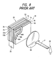
- Fig. 8 is a perspective view showing the prior art recording apparatus and recording head wherein a photoconductive layer 22 and a recording layer 12 separated are shown.
- a recording medium 10 capable of formation of a latent charge image, comprises the recording, layer 12, a transparent electrode layer 14, a color separation filter layer 16, and a glass base layer 18, which are laminated in order of mention.
- the recording head 20 comprises the photoconductive layer 22 including a carrier transport layer 22b and a carrier generation layer 22a, an electrode layer 24, and a base layer 26 which are laminated in order of mention.
- the recording medium 10 and the recording head 20 are arranged such that the recording layer 12 and the carrier transport layer 22b of the photoconductive layer 22 face each other with a given space.
- An optical image of an object 28 enters there through the glass base layer 18 of the recording medium 10 via the object lens 30.
- a power supply 32 with a given voltage is connected between the transparent electrode layer 14 and the electrode layer 24. It generates discharge between the recording layer 12 and photoconductive layer 22.
- the color separation filter layer 16 comprises thin bar-shaped filters 16R, 16G, and 16B arranged in order of mention for color-separation by transmitting primary color lights of red (R), green (G), and blue (B) by filters 16R, 16G, and 16B respectively.
- a charge retaining material for retaining charges on its surface or therein and photo-modulation member whose optical characteristic varies, can be used for the recording layer 12.
- the optical image of the object 28 enters the object lens 30 from the right of the drawing as shown by an arrow F and enters the photoconductive layer 22 of the recording head 20 through the object lens 30 and the recording medium 10.
- the filters 16R, 16G, and 16B of the color separation filter layer 16 separate the incident light into three primary colors. That is, the filter 16R allows only R component of the incident light to transmit therethrough; the filter 16G, only G component, and the filter 16B, only B component. That is, the filter layer 16 performs color separation. These color-separated transmitted light beams enter the photoconductive layer 22 through the transparent electrode layer 14 and the recording layer 12.
- the photoconductive layer 22 is formed by laminating the carrier transport layer 22b and the carrier generation layer 22a as mentioned above.
- the carrier transport layer 22b faces the recording layer 12.
- the color-separated light beams transmit the carrier transport layer 22b and enter the carrier generation layer 22a.
- the incident light beams are absorbed by the carrier generation layer 22a, so that carriers are generated in the carrier generation layer 22a.
- the potential of the power supply 32 is applied between the transparent electrode layer 14 and the electrode layer 24. Therefore, holes of the carriers generated in the carrier generation layer 22a move through the carrier transport layer 22b to a surface of the carrier transport layer 22b opposite to the recording layer 12.
- This movement produces a charge image corresponding to the optical image of the object 28 on the surface of the photoconductive layer 22.
- Such operation is made for each of separated light beams of R, G, and B, so that positive charge images are formed with respect to every separated light beam.
- This discharge produces a charge Q on the surface of the recording layer 12 and is accumulated and retained on its surface.
- the degree of the charge due to the discharge corresponds the positive charge image accumulated. Therefore, an image corresponding to the optical image of the object 28 is transferred on the surface of the recording layer 12.
- an amount of a charge per unit area on the recording layer is relates to an intensity of light per the unit area.
- a charge latent image corresponding to the optical image of the object 28 is recorded on the surface of the charge retaining layer of the recording medium 10.
- the positive charges on the charge retaining layer are produced for each of separated light beams, so that for each of the separated light beams of R, G, and B, a charge latent image is formed.
- the photo-modulation layer reacts to an electric field, so that an image is recorded as a change in optical characteristic of the photo-modulation layer.
- the present invention has been developed in order to remove the above-described drawbacks inherent to the conventional recording apparatus for recording information included in an electro-magnetic radiation-beam applied thereto and the conventional record head used for the same.
- a first recording apparatus for recording information included in an electro-magnetic radiation-beam applied thereto, comprising: a first electrode layer which transmits the electro-magnetic-beam incident thereto; a second electrode layer facing the first electrode layer for applying a given voltage between the first electrode layer and the same; a carrier generation layer provided between the first and second electrode layers responsive to the electromagnetic beam from the first electrode layer for generating carriers in accordance with intensity of the electromagnetic beam per unit area on the same; a carrier transport layer sandwiched between the carrier generation layer and the second electrode layer for transporting the carriers toward the second electrode layer in response to an electric field produced by application of the given voltage to the first and second electrode layers; and a recording layer provided between the first electrode layer and the carrier generation layer for recording the information by retaining charges developed by transportation of the carriers in the carrier transport layer, the recording layer transmitting the electro-magnetic beam from the first electrode layer.
- the recording layer and the carrier generation layer are spaced at a given distance or laminated with each other.
- the first recording apparatus may further comprises: color-separation filter including a set of plural different color filters, arranged in at least one direction for color-separating the electromagnetic beam, the color-separation filter arranged such that the electro-magnetic beam incident thereto enters the recording layer after color-separation by the same.
- a second recording apparatus for recording information included in an electro-magnetic radiation-beam applied thereto, comprising: a first electrode layer which transmits the electro-magnetic-beam incident thereto; a second electrode layer facing the first electrode layer for applying a given voltage between the first electrode layer and the same; a carrier generation layer provided between the first and second electrode layers responsive to the electro-magnetic beam from the first electrode layer for generating carriers in accordance with intensity of the electro-magnetic beam per unit area on the same; a carrier transport layer sandwiched between the carrier generation layer and the second electrode layer for transporting the carriers toward the second electrode in response to an electric field produced by application of the given voltage to the first and second electrode layers; and a photo-modulation layer provided between the first electrode layer and the carrier generation layer for recording the information by change in electro-optic characteristic thereof in response to the electric field modulated by the carriers transported in the carrier transport layer, the recording layer transmitting the electro-magnetic beam from the first electrode.
- the recording head for recording information included in an electro-magnetic radiation-beam applied thereto in a recording layer to be faced the same, the recording layer having a first electrode layer comprising: a second electrode layer; a carrier transport layer formed on the recording layer'side surface of the electrode layer; and a carrier generation layer formed on the carrier transport layer for generating carrier in response to the electro-magnetic radiation-beam transmitted through the recording layer in accordance with intensity of the electro-magnetic radiation-beam per unit area at the same, the carrier transport layer transporting the carrier toward the second electrode layer in response to application of a given voltage between the first and the second electrode layer, the recording layer recording the information by using the transported carriers and the application of the given voltage.
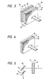
- Fig. 1 is a perspective view of a first embodiment of the invention of a recording apparatus and a recording head whose photoconductive layer 22 is separated from a recording layer 12.
- a recording medium 10 capable of formation of a latent charge image, comprises the recording layer 12, a transparent electrode layer 14, a color separation filter layer 16, and a glass base layer 18 which are laminated in order of mention.
- the recording medium 10 has the same structure as that of the prior art shown in Fig. 8.
- a recording head 40 comprises the photoconductive layer 22 including a carrier generation layer 22a and a carrier transport layer 22b, an electrode layer 24, and a base layer 26, which are laminated in order of mention.
- the arrangement of the carrier generation layer 22a and carrier transport layer 22b is different from that of the prior art of Fig. 8.
- the recording medium 10 and the recording head 40 are arranged such that the recording layer 12 and the photoconductive layer 22 face each other with a given space.
- An optical image of an object 28 enters the recording medium through the glass base layer 18 via the object lens 30.
- Fig. 2 is a perspective view of a second embodiment of the invention wherein the photoconductive layer 22 is laminated on the recording layer 12.
- the second embodiment of Fig. 2 has the same component as that shown in Fig. 1. That is, the second embodiment comprises the glass base layer 18, the color separation filter layer 16, the transparent electrode layer 14, the recording layer 12, the photoconductive layer 11 including the carrier generation layer 22a and the carrier transport layer 22b, and the electrode layer 24 are laminated in order of mention.
- the recording medium 10 and the recording head 40 are combined together by lamination.
- a power supply 32 is connected between the transparent electrode layer 14 and the electrode layer 24. It generates discharge between the recording layer 12 and the photoconductive layer 22.
- the color separation filter layer 16 comprises thin bar-shaped filters 16R, 16G, and 16B arranged in order of mention for transmitting primary color lights of red R, green G, and blue B respectively.
- a charge retaining material for example, a high resistance material such as a silicone resin and a material in which photoconductive fine particles are included in and near a surface of the resin, for retaining carriers on its surface or therein can be used as the recording layer 12.
- the light modulation material for example, a polymer dispersed liquid crystal film or PLZT (Lead Lanthanum Zirconate Titanate) which records information by change in optical characteristic in response to application of an electric field, can also be used as the recording layer 12.
- the light from the object 28 enters the object lens 30 from the right of the drawing as shown by an arrow F and enters the photoconductive layer 22 of the recording head 40 through the object lens 30 and the recording medium 10.
- the filters 16R, 16G, and 16B of the color separation filter layer 16 separates the incident light into three primary colors. That is, the filter 16R allows only R component of the incident light to transmit therethrough; the filter 16G, only G component, and the filter 16B, only B component. These color-separated transmitted light beams enter the photoconductive layer 22 through a transparent electrode layer 14 and the recording layer 12.
- the photoconductive layer 22 is formed by laminating the carrier generation layer 22a and the carrier transport layer 22b as mentioned above.
- the carrier generation layer 22a faces the recording layer 12.
- the incident light beams are absorbed by the carrier generation layer 22a, so that carriers are generated in the carrier generation layer 22a.
- a voltage of the power supply 32 is applied between the transparent electrode layer 14 and the electrode layer 24. Therefore, electrons of the carriers generated in the carrier generation layer 22a move through the carrier transport layer 22b toward the electrode layer 24 by an attraction force from plus polarity of the power supply 32.
- holes of carriers move to a surface of the carrier transport layer 22b opposite to the recording layer 12.
- This movement i.e., an electric field, produces a charge image corresponding to the optical image of the object 28 on the surface of the photoconductive layer 22.
- Such operation is performed for each of separated light beams of R, G, and B, so that positive charge images are formed for every separated light beam.
- a charge latent image of the optical image of the object 28 is recorded on the surface of the charge retaining layer.
- the positive charge on the charge retaining layer of the photoconductive layer 22 are produced for each of separated light beams, so that the charge latent images in the recording medium 10 are also formed for each of the separated light beams of R, G, and B.
- the photo-modulation layer reacts by the recording head 40, so that an image is recorded as a change in optical characteristic.
- the image can be recorded on the recording layer 12 directly without aerial discharge.
- the charge retaining material or the photo-modulation layer can be used for the recording layer 12.
- Fig. 3 is a perspective view of the third embodiment for illustrating the operation of reproducing by the recording layer 12 comprising the charge retaining material where a latent charge image is formed.
- the same elements as those shown in Figs. 1 and 2 are designated the same reference.
- a reproduce head 50 is arranged such that it faces the recording layer 12 comprising a charge retaining material where a latent charge image is formed.
- the reproduce head 50 comprises a photo-modulation layer 52 made of a photo-modulation material, an electrode layer 24, a base layer 26.
- the exposed surface of the light modulation layer 52 faces the recording layer 12 of the recording medium 10.
- a read-out beam L shown by an arrow enters the reproduce head 50 through the recording medium 10.
- white light is used as the read-out light L.
- the light modulation layer 52 produces phase difference between an ordinary ray and an extraordinary ray through electro-optical effect when the read-out light L enters there.
- a high polymer ⁇ liquid crystal composite film or PLZT and the like can be used for the photo-modulation layer whose optical characteristic is changed by application of an electric field.
- the charge image of the object 28 is formed on the recording medium 10 as mentioned as to Fig. 1.
- the reproduce head 50 is arranged near the recording medium 10.
- the transparent electrode layer 14 and 24 are connected the power supply 32, as shown.
- the electric field of the latent charge Q on the surface of the recording layer 12 effects the photo-modulation layer 52, so that electro-optical effect occurs in response to the incident light.
- the read-out light inters the recording medium 10 as shown by the arrow L
- the read-out light L is color-separated in to R, G, and B by the color separation filter 16 as the recording system mentioned above does. Therefore, the color-separated light R, G, and B enters the reproduce head 50 through the color-separation filter 16.
- electro-optical effect occurs in the light modulation layer 52, so that it enables the reproduction of color image of the object 28.
- Fig. 4 is a perspective view of the fourth embodiment of reproduction.
- the recording layer 12 is made of a photo-modulation material.
- the read-out light L transmits the color separation filter 16, enters the photo-modulation layer 12 made of the photo-modulation material, so that electro-optical effect developed provides a color image of the object directly.
- Fig. 5 is a perspective view of a fifth embodiment of reproducing.
- the dichroic mirrors 60 and 62 are provided in addition to the structure of the fourth embodiment.
- the read-out light L transmitted through the recording layer 12 comprising the color separation filter 16 and the photo-modulation layer enters the first dichroic mirror 60.
- the first dichroic mirror 60 only transmit a separation light beam G and reflects the remaining components R and B to the following dichroic mirror 62.
- the dichroic mirror 62 reflects separation light beam R and transmits a separation light beam B therethrough.
- the dichroic mirrors 60 and 62 separate the read-out light L into components R, G, and B. These components R, B, and B provide reproduction of color-separation image of the optical image of the object 28. If required, it can be converted into an electric signal by a photoelectric conversion means.
- the read-out light L can be projected on a surface two-dimensionally or by using scanning.
- Fig. 6 is an illustration for showing the sixth embodiment of reproducing for displaying a color image by directly projecting the read-out light L transmitted through the recording medium 10.
- This embodiment comprises the color separation filter 16 and the photo-modulation layer.
- the read-out light L transmitted through the recording layer 12 on which a latent charge image is formed is directly projected to a screen by a project lens 64.
- Fig. 7 is an illustration for illustrating a seventh embodiment.
- the read-out light L transmitted through the recording layer 12 on which a latent charge image is formed, comprising a photo-modulation layer is observed by the human eyes through the color separation filter 16.
Landscapes
- Physics & Mathematics (AREA)
- General Physics & Mathematics (AREA)
- Nonlinear Science (AREA)
- Mathematical Physics (AREA)
- Chemical & Material Sciences (AREA)
- Crystallography & Structural Chemistry (AREA)
- Optics & Photonics (AREA)
- Liquid Crystal (AREA)
- Combination Of More Than One Step In Electrophotography (AREA)
Applications Claiming Priority (2)
| Application Number | Priority Date | Filing Date | Title |
|---|---|---|---|
| JP112942/90 | 1990-04-27 | ||
| JP2112942A JPH049916A (ja) | 1990-04-27 | 1990-04-27 | 記録装置および記録ヘッド |
Publications (2)
| Publication Number | Publication Date |
|---|---|
| EP0459152A1 true EP0459152A1 (de) | 1991-12-04 |
| EP0459152B1 EP0459152B1 (de) | 1994-11-30 |
Family
ID=14599365
Family Applications (1)
| Application Number | Title | Priority Date | Filing Date |
|---|---|---|---|
| EP91106781A Expired - Lifetime EP0459152B1 (de) | 1990-04-27 | 1991-04-26 | Aufzeichnungsgerät zum Aufzeichnen von Informationen mit einem elektromagnetischen Richtstrahl und Aufzeichnungskopf hierfür |
Country Status (4)
| Country | Link |
|---|---|
| US (1) | US5161007A (de) |
| EP (1) | EP0459152B1 (de) |
| JP (1) | JPH049916A (de) |
| DE (1) | DE69105351T2 (de) |
Cited By (1)
| Publication number | Priority date | Publication date | Assignee | Title |
|---|---|---|---|---|
| US7252788B2 (en) | 2004-02-27 | 2007-08-07 | Dowa Mining Co., Ltd. | Phosphor, light source and LED |
Families Citing this family (23)
| Publication number | Priority date | Publication date | Assignee | Title |
|---|---|---|---|---|
| US5418096A (en) * | 1990-07-12 | 1995-05-23 | Dai Nippon Printing Co., Ltd. | Information recording medium and method of recording and reproducing electrostatic information |
| JPH04277716A (ja) * | 1991-03-06 | 1992-10-02 | Victor Co Of Japan Ltd | 情報記録媒体及び情報記録装置 |
| US5555205A (en) * | 1993-04-27 | 1996-09-10 | Dai Nippon Printing Co., Ltd. | Method device for recording information, and method for measuring the transmittance of liquid crystals, which is applied to recording information |
| US5638198A (en) * | 1994-11-22 | 1997-06-10 | Raphael Glass | Color filter in multiplicity of filaments for electronic displays |
| US7167155B1 (en) * | 1995-07-20 | 2007-01-23 | E Ink Corporation | Color electrophoretic displays |
| US7242513B2 (en) | 1997-08-28 | 2007-07-10 | E Ink Corporation | Encapsulated electrophoretic displays having a monolayer of capsules and materials and methods for making the same |
| US6839158B2 (en) | 1997-08-28 | 2005-01-04 | E Ink Corporation | Encapsulated electrophoretic displays having a monolayer of capsules and materials and methods for making the same |
| CA2320788A1 (en) | 1998-03-18 | 1999-09-23 | Joseph M. Jacobson | Electrophoretic displays and systems for addressing such displays |
| US6704133B2 (en) | 1998-03-18 | 2004-03-09 | E-Ink Corporation | Electro-optic display overlays and systems for addressing such displays |
| US6753999B2 (en) * | 1998-03-18 | 2004-06-22 | E Ink Corporation | Electrophoretic displays in portable devices and systems for addressing such displays |
| US7075502B1 (en) | 1998-04-10 | 2006-07-11 | E Ink Corporation | Full color reflective display with multichromatic sub-pixels |
| AU3987299A (en) | 1998-05-12 | 1999-11-29 | E-Ink Corporation | Microencapsulated electrophoretic electrostatically-addressed media for drawing device applications |
| CA2336596A1 (en) | 1998-07-08 | 2000-01-20 | E Ink Corporation | Methods for achieving improved color in microencapsulated electrophoretic devices |
| US6312304B1 (en) | 1998-12-15 | 2001-11-06 | E Ink Corporation | Assembly of microencapsulated electronic displays |
| US6504524B1 (en) | 2000-03-08 | 2003-01-07 | E Ink Corporation | Addressing methods for displays having zero time-average field |
| US6531997B1 (en) | 1999-04-30 | 2003-03-11 | E Ink Corporation | Methods for addressing electrophoretic displays |
| US7030412B1 (en) | 1999-05-05 | 2006-04-18 | E Ink Corporation | Minimally-patterned semiconductor devices for display applications |
| AU6365900A (en) | 1999-07-21 | 2001-02-13 | E-Ink Corporation | Use of a storage capacitor to enhance the performance of an active matrix drivenelectronic display |
| KR100767233B1 (ko) | 2000-04-18 | 2007-10-17 | 이 잉크 코포레이션 | 박막 트랜지스터의 제조 공정 및 기판 |
| US7893435B2 (en) | 2000-04-18 | 2011-02-22 | E Ink Corporation | Flexible electronic circuits and displays including a backplane comprising a patterned metal foil having a plurality of apertures extending therethrough |
| US20020060321A1 (en) | 2000-07-14 | 2002-05-23 | Kazlas Peter T. | Minimally- patterned, thin-film semiconductor devices for display applications |
| US6967640B2 (en) | 2001-07-27 | 2005-11-22 | E Ink Corporation | Microencapsulated electrophoretic display with integrated driver |
| US6900851B2 (en) | 2002-02-08 | 2005-05-31 | E Ink Corporation | Electro-optic displays and optical systems for addressing such displays |
Citations (6)
| Publication number | Priority date | Publication date | Assignee | Title |
|---|---|---|---|---|
| US3794418A (en) * | 1971-03-04 | 1974-02-26 | Xerox Corp | Imaging system |
| EP0120581A2 (de) * | 1983-02-15 | 1984-10-03 | Xerox Corporation | Schichtförmige photoempfindliche Abbildungsvorrichtung |
| EP0238094A1 (de) * | 1986-03-20 | 1987-09-23 | Minolta Camera Kabushiki Kaisha | Lichtempfindliches Element, bestehend aus einer Ladungstransportschicht und einer Ladungserzeugungsschicht |
| EP0301901A2 (de) * | 1987-07-29 | 1989-02-01 | Mita Industrial Co. Ltd. | Organisches, laminiertes, lichtempfindliches Material vom Typ der positiven Aufladung |
| EP0341668A1 (de) * | 1988-05-10 | 1989-11-15 | Victor Company Of Japan, Limited | Vorrichtung zur Aufnahme und Wiedergabe vom latenten Ladungsbild |
| EP0369794A2 (de) * | 1988-11-16 | 1990-05-23 | Victor Company Of Japan, Ltd. | Optisches Aufzeichnungsmedium und Aufnahme-/Wiedergabesystem |
Family Cites Families (14)
| Publication number | Priority date | Publication date | Assignee | Title |
|---|---|---|---|---|
| JPH0233273A (ja) * | 1988-07-22 | 1990-02-02 | Victor Co Of Japan Ltd | 撮像装置 |
| FR2157060A6 (de) * | 1971-10-15 | 1973-06-01 | Labo Electronique Physique | |
| US3723651A (en) * | 1971-12-27 | 1973-03-27 | Rca Corp | Optically-scanned liquid-crystal projection display |
| US3957349A (en) * | 1974-07-29 | 1976-05-18 | Xerox Corporation | Imaging method |
| US3932025A (en) * | 1974-10-25 | 1976-01-13 | Xerox Corporation | Imaging system |
| JPS60144721A (ja) * | 1984-01-06 | 1985-07-31 | Canon Inc | 画像形成装置 |
| US4712878A (en) * | 1985-01-18 | 1987-12-15 | Canon Kabushiki Kaisha | Color image forming apparatus comprising ferroelectric smectic liquid crystal having at least two stable states |
| US4831452A (en) * | 1986-12-30 | 1989-05-16 | Victor Company Of Japan Ltd. | Image pickup device having a photoconductive optical modulator element |
| US4956714A (en) * | 1988-01-24 | 1990-09-11 | Victor Company Of Japan, Ltd. | Image pickup apparatus |
| IL90230A (en) * | 1988-05-13 | 1993-01-31 | Victor Company Of Japan | Image pickup apparatus |
| JPH0222924A (ja) * | 1988-07-12 | 1990-01-25 | Matsushita Electric Ind Co Ltd | 位相同期発振器 |
| DE68921686T2 (de) * | 1988-08-19 | 1995-07-27 | Victor Company Of Japan | Wiedergabegerät für ein Ladungslatentbildaufzeichnungsmedium. |
| US5006935A (en) * | 1988-09-26 | 1991-04-09 | Victor Company Of Japan, Ltd. | Charge latent image recording reproducing system with a uniformly charge detection region providing a reference intensity of a recorded object |
| JPH02306790A (ja) * | 1989-05-22 | 1990-12-20 | Victor Co Of Japan Ltd | 記録再生装置 |
-
1990
- 1990-04-27 JP JP2112942A patent/JPH049916A/ja active Pending
-
1991
- 1991-04-25 US US07/691,614 patent/US5161007A/en not_active Expired - Fee Related
- 1991-04-26 DE DE69105351T patent/DE69105351T2/de not_active Expired - Fee Related
- 1991-04-26 EP EP91106781A patent/EP0459152B1/de not_active Expired - Lifetime
Patent Citations (6)
| Publication number | Priority date | Publication date | Assignee | Title |
|---|---|---|---|---|
| US3794418A (en) * | 1971-03-04 | 1974-02-26 | Xerox Corp | Imaging system |
| EP0120581A2 (de) * | 1983-02-15 | 1984-10-03 | Xerox Corporation | Schichtförmige photoempfindliche Abbildungsvorrichtung |
| EP0238094A1 (de) * | 1986-03-20 | 1987-09-23 | Minolta Camera Kabushiki Kaisha | Lichtempfindliches Element, bestehend aus einer Ladungstransportschicht und einer Ladungserzeugungsschicht |
| EP0301901A2 (de) * | 1987-07-29 | 1989-02-01 | Mita Industrial Co. Ltd. | Organisches, laminiertes, lichtempfindliches Material vom Typ der positiven Aufladung |
| EP0341668A1 (de) * | 1988-05-10 | 1989-11-15 | Victor Company Of Japan, Limited | Vorrichtung zur Aufnahme und Wiedergabe vom latenten Ladungsbild |
| EP0369794A2 (de) * | 1988-11-16 | 1990-05-23 | Victor Company Of Japan, Ltd. | Optisches Aufzeichnungsmedium und Aufnahme-/Wiedergabesystem |
Non-Patent Citations (1)
| Title |
|---|
| PATENT ABSTRACTS OF JAPAN vol. 15, no. 98 (E-1042)(4626), 8 March 1991; & JP - A - 2306790 (VICTOR COMP. OF JAPAN) 20.12.1990 * |
Cited By (1)
| Publication number | Priority date | Publication date | Assignee | Title |
|---|---|---|---|---|
| US7252788B2 (en) | 2004-02-27 | 2007-08-07 | Dowa Mining Co., Ltd. | Phosphor, light source and LED |
Also Published As
| Publication number | Publication date |
|---|---|
| DE69105351D1 (de) | 1995-01-12 |
| DE69105351T2 (de) | 1995-04-06 |
| EP0459152B1 (de) | 1994-11-30 |
| JPH049916A (ja) | 1992-01-14 |
| US5161007A (en) | 1992-11-03 |
Similar Documents
| Publication | Publication Date | Title |
|---|---|---|
| US5161007A (en) | Recording head with carrier generation and transport layers adjacent a photo-modulation layer for recording information included in an electro-magnetic radiation-beam applied thereto | |
| EP0450952B1 (de) | Optische Einrichtung für die Farbbilddarstellung | |
| EP0307203B1 (de) | Optisches System zur Trennung dreier Farben | |
| EP0444663B1 (de) | Farbbilderzeugungssystem | |
| US3946433A (en) | Phase image scanning method | |
| JP2990828B2 (ja) | 情報記録媒体 | |
| EP0376282B1 (de) | Verfahren zur optischen Modulation und Vorrichtung zur Wiedergabe eines latenten Ladungsbildes | |
| JPS63168618A (ja) | 撮像装置 | |
| EP0326347A2 (de) | Bildaufnahmevorrichtung | |
| JPH02306790A (ja) | 記録再生装置 | |
| US3935589A (en) | Color television signal generator | |
| US5185617A (en) | Method of information conversion and apparatus thereof | |
| US5055936A (en) | Charge latent image recording medium and recording/reproducing apparatus thereof | |
| US5144415A (en) | Apparatus for processing information carried by electro-magnetic radiation beam | |
| JPH0318815A (ja) | 光―光変換素子 | |
| JPH04274027A (ja) | 電磁放射線情報記録装置 | |
| JPH04218055A (ja) | 複数情報の記録媒体 | |
| EP0646851B1 (de) | Farbbilderzeugungssystem | |
| SU1094018A1 (ru) | Устройство дл электромагнитной фотозаписи | |
| JPH0787555B2 (ja) | 撮像装置 | |
| JPS63168631A (ja) | カラ−撮像装置 | |
| JP2677051B2 (ja) | 情報記録媒体 | |
| JP2897588B2 (ja) | 表示装置 | |
| JPH0435355A (ja) | スキャナ | |
| JPH0229173A (ja) | 静電潜像の記録再生方法 |
Legal Events
| Date | Code | Title | Description |
|---|---|---|---|
| PUAI | Public reference made under article 153(3) epc to a published international application that has entered the european phase |
Free format text: ORIGINAL CODE: 0009012 |
|
| AK | Designated contracting states |
Kind code of ref document: A1 Designated state(s): DE FR GB |
|
| 17P | Request for examination filed |
Effective date: 19911209 |
|
| 17Q | First examination report despatched |
Effective date: 19930504 |
|
| GRAA | (expected) grant |
Free format text: ORIGINAL CODE: 0009210 |
|
| AK | Designated contracting states |
Kind code of ref document: B1 Designated state(s): DE FR GB |
|
| REF | Corresponds to: |
Ref document number: 69105351 Country of ref document: DE Date of ref document: 19950112 |
|
| ET | Fr: translation filed | ||
| PLBE | No opposition filed within time limit |
Free format text: ORIGINAL CODE: 0009261 |
|
| STAA | Information on the status of an ep patent application or granted ep patent |
Free format text: STATUS: NO OPPOSITION FILED WITHIN TIME LIMIT |
|
| 26N | No opposition filed | ||
| PGFP | Annual fee paid to national office [announced via postgrant information from national office to epo] |
Ref country code: FR Payment date: 20000411 Year of fee payment: 10 |
|
| PGFP | Annual fee paid to national office [announced via postgrant information from national office to epo] |
Ref country code: GB Payment date: 20000426 Year of fee payment: 10 |
|
| PGFP | Annual fee paid to national office [announced via postgrant information from national office to epo] |
Ref country code: DE Payment date: 20000427 Year of fee payment: 10 |
|
| PG25 | Lapsed in a contracting state [announced via postgrant information from national office to epo] |
Ref country code: GB Free format text: LAPSE BECAUSE OF NON-PAYMENT OF DUE FEES Effective date: 20010426 |
|
| PG25 | Lapsed in a contracting state [announced via postgrant information from national office to epo] |
Ref country code: FR Free format text: THE PATENT HAS BEEN ANNULLED BY A DECISION OF A NATIONAL AUTHORITY Effective date: 20010430 |
|
| GBPC | Gb: european patent ceased through non-payment of renewal fee |
Effective date: 20010426 |
|
| PG25 | Lapsed in a contracting state [announced via postgrant information from national office to epo] |
Ref country code: DE Free format text: LAPSE BECAUSE OF NON-PAYMENT OF DUE FEES Effective date: 20020201 |
|
| REG | Reference to a national code |
Ref country code: FR Ref legal event code: ST |