EP0458030A1 - Correction de défaut pour des capteurs d'images à CCD et CID - Google Patents
Correction de défaut pour des capteurs d'images à CCD et CID Download PDFInfo
- Publication number
- EP0458030A1 EP0458030A1 EP91104360A EP91104360A EP0458030A1 EP 0458030 A1 EP0458030 A1 EP 0458030A1 EP 91104360 A EP91104360 A EP 91104360A EP 91104360 A EP91104360 A EP 91104360A EP 0458030 A1 EP0458030 A1 EP 0458030A1
- Authority
- EP
- European Patent Office
- Prior art keywords
- pixel data
- pixel
- data
- frame buffer
- dark
- Prior art date
- Legal status (The legal status is an assumption and is not a legal conclusion. Google has not performed a legal analysis and makes no representation as to the accuracy of the status listed.)
- Granted
Links
Images

Classifications
-
- H—ELECTRICITY
- H04—ELECTRIC COMMUNICATION TECHNIQUE
- H04N—PICTORIAL COMMUNICATION, e.g. TELEVISION
- H04N25/00—Circuitry of solid-state image sensors [SSIS]; Control thereof
- H04N25/60—Noise processing, e.g. detecting, correcting, reducing or removing noise
- H04N25/68—Noise processing, e.g. detecting, correcting, reducing or removing noise applied to defects
- H04N25/683—Noise processing, e.g. detecting, correcting, reducing or removing noise applied to defects by defect estimation performed on the scene signal, e.g. real time or on the fly detection
Definitions
- This invention relates generally to a system and method of defect correction in solid state imagers and, more particularly, to charge coupled device (CCD) and charge injection device (CID) imagers employing a pixel correction circuit with reduced memory requirements.
- CCD charge coupled device
- CID charge injection device
- Charge coupled imaging devices and charge injection imaging devices comprising a plurality of photosensitive elements arranged in a matrix of rows and columns are well known in the art.
- Each of the photosensitive elements comprises row and column electrodes. All of the row electrodes in each row are in common connection with respect to each other, and all of the column electrodes in each column are in common connection with respect to each other also.
- Incident scene light operates to photogenerate minority charge carriers in potential wells under each pair of electrodes in each photosensitive element.
- the photogenerated charges may be transferred out of the imager as a pulse train of analog voltages by well known scanning techniques.
- the analog signals may thereafter be color or gamma corrected digitized and stored in a buffer memory.
- dead spots within a photo array are detected based upon excessive rate of change in sequentially accessed prestored digital sensitivity correction coefficients corresponding to the array of photosensitive elements.
- the leading and trailing edges of dead spots are detected by comparing arithmetic differences between successive correction coefficients to predetermined threshold values.
- the last video signal value is employed to fill in the dead spots.
- U.S. Patent No. 4,802,011 describes a correction circuit in which a defective picture pickup element is replaced by a proceeding, non-defective picture pickup element employing a signal sampling circuit and a real time video signal.
- Bencuya et al. U.S. Patent No. 4,843,473, assigned to the assignee herein, describes a charge injection device with low noise readout in which KTC and fixed pattern noise are subtracted from the signals retrieved from the charge injection imaging device.
- Patent No. 4,734,774 describes a CCD image defect compensation circuit in which adjacent streams of data are compared and corrected by replacement of adjacent data.
- a threshold detector looks at the combined image pulse and the fixed pattern noise (or dark current) of the pixel. If a given threshold is exceeded the pixel information is discarded and some other value is substituted therein.
- An example of such an approach is shown in Endo et al., U.S. Patent No. 4,567,525.
- a problem with this approach is similar to that encountered with frequency sensitive systems in which a sharp transition or increase in the pixel response may be due to a line in the picture as opposed to a bad element.
- Some of the described prior arrangements employ circuitry which is complicated and requires additional storage devices for handling the defect information. Some arrangements sense the real time image data signals in order to determine whether a defect exists even though image data varies from image scene to image scene. It is thus difficult to correlate or correct for the defects, especially in cases where the defect do not always appear. For example, as scene light Changes or as temperature varies.
- defect correcting apparatus for a CID or CCD imaging device in which defect correction is independent of the incident scene light.
- the present invention is devised to obviate the shortcomings of the prior art by producing an online or real time method of detecting bad pixels without ambiguity.
- the pixel data from an imaging device does not exceed a threshold indicative of a defect
- the pixel data from the scene is stored in a buffer. If the dark pixel data exceeds a threshold the image scene data from a prior pixel is entered in the buffer whereby pixel correction is achieved.
- a defect correction apparatus for a solid state imaging device comprises a frame buffer responsively coupled to the imaging device for storing digital values of shuttered dark pixel data from image locations of the imaging device.
- a register responsively coupled to the imaging device and having an output coupled to the frame buffer sequentially clocks digital values of image pixel data of the imaging device into the frame buffer.
- a comparator having an output operatively coupled to the register and being responsively coupled to the dark pixel data of the frame buffer produces enable and inhibit outputs. When any selected element of dark pixel data is less than a threshold, indicative of an operative pixel element in the imaging device, data stored in the register corresponding the pixel is stored in the frame buffer in response to the enable signal. When the value of the dark pixel data in the frame buffer is greater than the threshold the comparator produces an inhibit signal. The value of image data of a previous operative pixel element is thereby entered into the register and frame buffer.
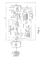
- a circuit for detecting and correcting for pixel defects in a charge injection device 12 in the form of an array of light sensitive elements or pixels 14.
- CID charge injection device
- an absolute measure of the dark current or fixed pattern noise associated with each pixel 14 in the CID 12 is first established by shuttering the CID 12 and reading dark pixel data of each pixel 14 produced thereby into a frame buffer 16.
- a digital representation of the dark current of each pixel 14 is stored in the frame buffer 16 at addresses corresponding to the location of each pixel 14 in the CID array 12.
- pixel data from the CID is input to the frame buffer 16 on a pixel by pixel basis for each corresponding location therein. If the dark current data stored in the frame buffer 16 at any particular pixel location exceeds a given threshold indicative of a bad or defective pixel, image scene data from the prior pixel is substituted therefor in the frame buffer.
- the CID 12 is shuttered and dark current signals in the CID are allowed to stabilize for a selected period of time, for example, 30 microseconds.
- Clock pulses to input 18 cause the CID 12 to clock out analog pixel data on a pixel by pixel basis to a level shifting device 20 which matches the voltage or current produced by the CID 12 to the correction circuitry 10.
- the output of the level shifting device 20 is coupled to the non inverting (+) input 21 of an automatic gain control amplifier (AGC) 22.
- AGC 22 automatic gain control amplifier
- the output 23 of the AGC 22 is coupled alternately to a gamma correction circuit 24 through a switch contact 26 or directly to an analog to digital converter (A/D) 28 via switch contact 30.
- the contacts 26 and 30 are alternately opened and closed by a gamma switch control 32 governed by a gamma clock input 31.
- the pixel data is converted by A/D 28 to a digital value for storage in an output register 34.
- the output register 34 is coupled to the frame buffer 16 for clocking in digital values of the CID pixels 14 in accordance with pulses on write input (W) 36 and clock input 37 of the frame buffer 16.
- a digital to analog converter (D/A) 38 is coupled to the output 40 of frame buffer 16 and senses the dark current data stored therein for each address on a pixel by pixel basis in accordance with pulses on read input (R) 39 and clock input 37.
- the D/A 38 converts the digital value of the dark current produced by the frame buffer 16 to an analog signal and couples the analog signal to the inverting (-) input 41 of the AGC amplifier 22 as shown.
- the analog data from the CID 12, representative of a subsequently exposed image scene for any selected pixel 14 is coupled to the AGC 22 the corresponding data representative of dark current from D/A 38, is coupled to the AGC 22.
- the two analog signals are subtracted whereby only the net data representative of the image scene light may be converted to a digital value in A/D 28 and subsequently stored in the frame buffer 16, provided the dark current data meets a required threshold criterion discussed hereinafter.
- a comparator 42 operatively coupled to A/D 28, is responsive to dark pixel (DP) data stored in the frame buffer 16 and to a threshold (Th) 44. If the dark pixel data does not exceed the threshold, the A/D 28 is enabled. More specifically, the output register 34 is clocked to receive therein the digital value of the image scene data. As a result, the digital data produced by A/D 28 is stored in the register 34, thereby replacing any data currently stored therein. Information in the output register 34 is read into frame buffer 16 in response to a write pulse 36.
- the A/D 28 is inhibited, that is, output register 34 is not clocked. Therefore, the current data representation of the prior pixel is retained in the register 34 and thereafter read into the frame buffer 16. Thus, if a particular pixel (n) is defective, the data from the previous pixel (n-1) is substituted for the actual data produced by such defective pixel.
- a picture is taken by exposing the imager 12 to scene light in which photogenerated charges are produced and stored as analog pixel data.
- the imager 12, in response to clock pulses 18 produces a stream of analog image pulses representative of the pixel data for each pixel 14.
- the image scene data from each pixel 14 location 1, 2, 3..., n-1, n is sequentially converted to digital values at A/D converter 28 and thereafter stored in output register 34 on a pixel by pixel basis prior to entry to frame buffer 16. If the output register 34 has current (n-1) scene data stored therein, when the A/D 28 and output register 34 is next enabled and clocked, new digital data for the next pixel in the sequence, namely (n), is clocked into register 34.
- A/D 28 and register 34 are respectively enabled and clocked only if the comparator 42 produces an enable pulse in response to a dark pixel (DP) input which is less than the threshold (Th). Otherwise the current data (n-1) remains in the output register 34 and current data (n) is discarded. In other words, if DP ⁇ Th, then the output 46 of comparator 42 enables A/D 28 and the register 34 is clocked. As a consequence, image scene data from the n pixel location is clocked in to register 34 and thereafter replaces the dark pixel DP from the n location in the frame buffer 16. If DP > Th then, the comparator output 46 disables A/D 28 and the register 34 is not clocked.
- a white balance control circuit (WBC) 54 has an output 56 coupled to the AGC 22 as shown.
- Clock input 58 and level set input 60 coupled to inputs of the WBC 54 receive appropriately timed signals in order to vary the gain or level of the AGC 22 in accordance with known techniques. For example, as is often typical for a color scene the first line of pixels 14 in the CID 12 represents the red, the next line the blue and the next line the green. Accordingly, the WBC 54 output 56 is level shifted to the appropriate level on a line by line basis.
- the appropriate level set input 60 may be a preselected fixed value for each line. Alternatively, level set 60 may be variable and set by a device responsive to the particular scene condition, for example, a light meter, not shown. Pulses to the clock input 58 drive the white balance control 54 and thereby enable it to change the gain of the AGC on a line-by-line basis as described or, if desired, on a pixel by pixel basis.
- Fig. 2 in which similar elements are referred to by the same reference numbers referred to in Fig. 1, employs a charge coupled device (CCD) imager 12. Operation of the arrangement in Fig. 2 is the same as Fig. 1 except that a dark current correction signal is not provided to the inverting input of AGC 22, because CCDs produce less dark current and, therefore, it may not be necessary to provide such correction. However, in accordance with teachings of the invention dark currents above an appropriate threshold are indicative of a defective pixel and the prior pixel data is substituted therefor when required.
- CCD charge coupled device
- a shuttering pulse is produced which charges the CID to a dark pixel level indicative of zero scene light.
- the signal is level shifted at 20 to an appropriate level and coupled to AGC 22 via its non inverting input 21 and thence through closed switch 30 directly to the A/D converter 28.
- the gamma switch 32 is actuated by shutter pulse (S) so that switch 30 is closed and switch 26 is opened thereby bypassing the gamma control 24.
- S shutter pulse
- the A/D converter 28 is always enabled by shutter pulse (S) and input 29 so that all dark pixel DP data (1, 2, 3... n) for each corresponding pixel 14 is clocked into the frame buffer 16 regardless of its level.
- the inverting input 41 to the AGC 22 is open by a shutter pulse (S) to D/A clock input 29 so that dark current data is coupled directly to the frame buffer 16 without adjustment.
- the CID 12 may be exposed to image scene light.
- the image scene pixel data is coupled to the correction circuit 10 via the level shift circuit 20 as aforesaid.
- the gamma control switch 32 may be actuated by the absence of the (S) pulse to its enable input 31 so that the switch 30 is open and switch 26 is closed. Accordingly, the output of the AGC 22 is coupled via the gamma correction circuit 24 to the A/D converter 28.
- the D/A converter 38 (is enabled by the absence of the (S) pulse) and dark current DP pixel data appearing at the output 40 of the frame buffer 16 is converted to an analog signal by D/A 38 which signal is input to the inverting input 41 of AGC 22.
- the net gamma corrected signal namely the image scene data minus the dark current DP is analog-to-digital converted by A/D 28 for storage in the frame buffer 16.
- the dark current data DP from the frame buffer 16 at the same time is read by the comparator 42 and compared to the threshold Th.
- A/D converter 28 is, as a consequence, either enabled or disabled depending upon the level of the dark current data.
- the analog value of the n pixel data is converted to a digital value and is clocked into register 34 for entry into buffer 16. If the pixel is defective the A/D converter 28 is not enabled and the register 34 is consequently not clocked. Accordingly, the n-1 data currently in the register 34 is read into the frame buffer 16 for the n location.
- the comparator 42 and D/A converter 38 are enabled during frame buffer read pulse so that the input signal from the n pixel may be corrected.
- the D/A 38 and comparator 42 are enabled for a time sufficient to preserve the input signal, to allow the D/A conversion to occur and to maintain a correction signal on the AGC 22 so that information is accurately presented to the A/D converter 28.
- Comparator 42 looks at the output 40 of the frame buffer 16 and the threshold Th 44 and produces an enable signal if DP ⁇ Th. If the enable signal is produced, the data from the AGC 22 is A/D converted and clocked into the register 34. If the threshold Th is exceeded, the comparator 42 produces no output and the current data from the n-1 pixel stored in the output register 34 remains therein. Thereafter, in either case, the data stored in the register 34 is then written into the frame buffer 16 in accordance with the frame buffer write input 36. The data on the output register 34 is stored therein until clocked out by the next enable signal from the comparator 42.
- Fig. 2 The arrangement of Fig. 2 is sequenced in a manner similar to the arrangement of Fig. 1 herein described. The exception is that the D/A feedback loop is not employed for the AGC 22.
Applications Claiming Priority (2)
| Application Number | Priority Date | Filing Date | Title |
|---|---|---|---|
| US528123 | 1990-05-24 | ||
| US07/528,123 US5047863A (en) | 1990-05-24 | 1990-05-24 | Defect correction apparatus for solid state imaging devices including inoperative pixel detection |
Publications (2)
| Publication Number | Publication Date |
|---|---|
| EP0458030A1 true EP0458030A1 (fr) | 1991-11-27 |
| EP0458030B1 EP0458030B1 (fr) | 1994-12-14 |
Family
ID=24104352
Family Applications (1)
| Application Number | Title | Priority Date | Filing Date |
|---|---|---|---|
| EP91104360A Expired - Lifetime EP0458030B1 (fr) | 1990-05-24 | 1991-03-20 | Correction de défaut pour des capteurs d'images à CCD et CID |
Country Status (9)
| Country | Link |
|---|---|
| US (1) | US5047863A (fr) |
| EP (1) | EP0458030B1 (fr) |
| JP (1) | JPH0670238A (fr) |
| AT (1) | ATE115811T1 (fr) |
| CA (1) | CA2038914A1 (fr) |
| DE (1) | DE69105815T2 (fr) |
| DK (1) | DK0458030T3 (fr) |
| ES (1) | ES2068411T3 (fr) |
| GR (1) | GR3015401T3 (fr) |
Cited By (3)
| Publication number | Priority date | Publication date | Assignee | Title |
|---|---|---|---|---|
| DE4419068A1 (de) * | 1993-06-02 | 1994-12-08 | Hitachi Ltd | Videokamera mit einer Funktion zum Korrigieren defekter Pixel einer Bildaufnahmevorrichtung vom Halbleitertyp und ein Verfahren zum Korrigieren defekter Pixel einer Bildaufnahmevorrichtung vom Halbleitertyp |
| EP1155308A1 (fr) * | 1999-02-23 | 2001-11-21 | Direct Radiography Corp. | Traitement des pixels defectueux dans un detecteur de rayonnement |
| WO2003067900A1 (fr) * | 2002-02-04 | 2003-08-14 | Pilz Gmbh & Co. | Procede destine a verifier la securite fonctionnelle d'un capteur d'images ainsi que dispositif dote d'un capteur d'images |
Families Citing this family (40)
| Publication number | Priority date | Publication date | Assignee | Title |
|---|---|---|---|---|
| JPH0828811B2 (ja) * | 1988-05-10 | 1996-03-21 | 富士写真フイルム株式会社 | 画像入力装置 |
| DE69116905T2 (de) * | 1990-03-13 | 1996-06-13 | Sony Corp | Schattierungseffektenkorrekturvorrichtung |
| JPH05508529A (ja) * | 1991-05-10 | 1993-11-25 | イーストマン・コダック・カンパニー | 電子式画像化のための注文製作可能なタイミング及び制御asic |
| US5291293A (en) * | 1992-06-01 | 1994-03-01 | Eastman Kodak Company | Electronic imaging device with defect correction |
| US5235412A (en) * | 1992-08-17 | 1993-08-10 | Eastman Kodak Company | Electronic color imaging system and analog signal processor therefor |
| US5694228A (en) * | 1994-08-09 | 1997-12-02 | Ricoh Company,Ltd. | Document image processor with defect detection |
| US5499114A (en) * | 1994-10-31 | 1996-03-12 | Eastman Kodak Company | Digital image scanning apparatus with pixel data compensation for bad photosites |
| US5657400A (en) * | 1995-01-31 | 1997-08-12 | General Electric Company | Automatic identification and correction of bad pixels in a large area solid state x-ray detector |
| US5990939A (en) * | 1995-09-28 | 1999-11-23 | Raytheon Company | Video demultiplexing interface for a missile tracking system |
| US6061092A (en) * | 1997-12-05 | 2000-05-09 | Intel Corporation | Method and apparatus for dark frame cancellation for CMOS sensor-based tethered video peripherals |
| JP3587433B2 (ja) * | 1998-09-08 | 2004-11-10 | シャープ株式会社 | 固体撮像素子の画素欠陥検出装置 |
| US6381374B1 (en) * | 1998-10-30 | 2002-04-30 | General Electric Company | Histogram analysis method for defective pixel identification |
| JP3532781B2 (ja) * | 1999-02-12 | 2004-05-31 | 株式会社メガチップス | 画像入力装置の画像処理回路 |
| JP4199874B2 (ja) * | 1999-03-30 | 2008-12-24 | 富士フイルム株式会社 | 画像処理装置及び処理方法 |
| US7324143B1 (en) | 1999-04-13 | 2008-01-29 | Rochester Institute Of Technology | Method and system for reducing noise in a digital image and apparatus thereof |
| AU4079800A (en) * | 1999-04-13 | 2000-11-14 | Rochester Institute Of Technology | Method and system for reducing noise in a digital image and apparatus thereof |
| US6661456B1 (en) | 1999-04-30 | 2003-12-09 | General Electric Company | Imaging of pixel defects in digital detectors |
| US7140766B2 (en) * | 1999-08-04 | 2006-11-28 | Given Imaging Ltd. | Device, system and method for temperature sensing in an in-vivo device |
| US6654054B1 (en) | 1999-11-02 | 2003-11-25 | Agilent Technologies, Inc. | Method and apparatus for canceling the effects of noise in an electronic signal |
| US6792159B1 (en) | 1999-12-29 | 2004-09-14 | Ge Medical Systems Global Technology Company, Llc | Correction of defective pixels in a detector using temporal gradients |
| US7068854B1 (en) | 1999-12-29 | 2006-06-27 | Ge Medical Systems Global Technology Company, Llc | Correction of defective pixels in a detector |
| US6768512B1 (en) * | 2000-07-12 | 2004-07-27 | Vanguard International Semiconductor Corp. | Method of bad pixel correction |
| JP2002354340A (ja) * | 2001-05-24 | 2002-12-06 | Olympus Optical Co Ltd | 撮像装置 |
| US6737625B2 (en) | 2001-06-28 | 2004-05-18 | Agilent Technologies, Inc. | Bad pixel detection and correction in an image sensing device |
| US6623161B2 (en) | 2001-08-28 | 2003-09-23 | Ge Medical Systems Global Technology Company, Llc | Method and apparatus for identifying and correcting line artifacts in a solid state X-ray detector |
| US6663281B2 (en) | 2001-09-25 | 2003-12-16 | Ge Medical Systems Global Technology Company, Llc | X-ray detector monitoring |
| US6974973B2 (en) * | 2002-11-08 | 2005-12-13 | Micron Technology, Inc. | Apparatus for determining temperature of an active pixel imager and correcting temperature induced variations in an imager |
| US6919568B2 (en) | 2003-04-08 | 2005-07-19 | Ge Medical Systems Global Technology Company Llc | Method and apparatus for identifying composite defective pixel map |
| EP1594308A1 (fr) * | 2004-05-07 | 2005-11-09 | Dialog Semiconductor GmbH | Correction de pixels RGB défectueux dans une ligne unique d'un filtre Bayer |
| US20060262210A1 (en) * | 2005-05-19 | 2006-11-23 | Micron Technology, Inc. | Method and apparatus for column-wise suppression of noise in an imager |
| JP4351658B2 (ja) * | 2005-07-21 | 2009-10-28 | マイクロン テクノロジー, インク. | メモリ容量低減化方法、メモリ容量低減化雑音低減化回路及びメモリ容量低減化装置 |
| JP2008048104A (ja) | 2006-08-14 | 2008-02-28 | Sony Corp | 撮像装置と欠陥補正回路および欠陥補正方法 |
| US7796806B2 (en) * | 2006-09-25 | 2010-09-14 | Nokia Corporation | Removing singlet and couplet defects from images |
| DE102007013620A1 (de) * | 2007-03-21 | 2008-09-25 | Siemens Ag | Vorrichtung und Verfahren zur Überwachung von Festkörperdetektoren |
| US20100231763A1 (en) * | 2009-03-16 | 2010-09-16 | Harris Corporation, Corporation Of The State Of Delaware | Defective pixel detector for a digital video camera and associated methods |
| JP5521460B2 (ja) * | 2009-09-18 | 2014-06-11 | ソニー株式会社 | 撮像装置および方法、電子機器、並びにプログラム |
| WO2012063265A2 (fr) | 2010-11-12 | 2012-05-18 | Indian Institute Of Technology, Kharagpur | Procédé et appareil de détection de mauvais pixels dans un réseau de capteurs et d'annulation de l'erreur |
| WO2013007295A1 (fr) | 2011-07-11 | 2013-01-17 | Fraunhofer-Gesellschaft zur Förderung der angewandten Forschung e.V. | Appareil de caméra et caméra |
| US8830361B2 (en) | 2012-04-12 | 2014-09-09 | Taiwan Semiconductor Manufacturing Company, Ltd. | Method of reducing column fixed pattern noise |
| US9014504B2 (en) * | 2012-05-31 | 2015-04-21 | Apple Inc. | Systems and methods for highlight recovery in an image signal processor |
Citations (10)
| Publication number | Priority date | Publication date | Assignee | Title |
|---|---|---|---|---|
| US4535359A (en) | 1983-01-17 | 1985-08-13 | Eastman Kodak Company | Defect correction in solid state imaging |
| US4567525A (en) | 1983-10-18 | 1986-01-28 | Kabushiki Kaisha Toshiba | CCD Picture element defect compensating apparatus |
| US4590520A (en) | 1983-11-28 | 1986-05-20 | Ball Corporation | Method and apparatus for detecting and filling-in dead spots of video signals from an image sensor |
| US4701784A (en) | 1984-06-01 | 1987-10-20 | Matsushita Electric Industrial Co., Ltd. | Pixel defect correction apparatus |
| US4734774A (en) | 1981-08-14 | 1988-03-29 | Texas Instruments Incorporated | CCD imager video output defect compensation |
| US4802011A (en) | 1986-06-24 | 1989-01-31 | U.S. Philips Corp. | Picture pick-up device with an image sensor in the form of a charge transfer device |
| US4805013A (en) | 1984-09-05 | 1989-02-14 | Canon Kabushiki Kaisha | Image data conversion system |
| US4843473A (en) | 1988-03-21 | 1989-06-27 | Polaroid Corporation | Charge injection device with low noise readout |
| US4858013A (en) * | 1987-03-19 | 1989-08-15 | Mitsubishi Denki Kabushiki Kaisha | Solid state imaging device with adaptive pixel correction |
| EP0350328A2 (fr) * | 1988-07-08 | 1990-01-10 | Xerox Corporation | Correction d'offset, de gain et de mauvais éléments d'images dans un réseau de balayage électronique |
Family Cites Families (10)
| Publication number | Priority date | Publication date | Assignee | Title |
|---|---|---|---|---|
| JPS6013549B2 (ja) * | 1977-01-14 | 1985-04-08 | ソニー株式会社 | 固体撮像装置の雑音除去回路 |
| US4200939A (en) * | 1977-10-19 | 1980-05-06 | Codman & Shurtleff, Inc. | Method for fixation of prostheses to bone |
| JPS5919513B2 (ja) * | 1978-01-20 | 1984-05-07 | 株式会社東芝 | 固体撮像方式 |
| US4216503A (en) * | 1979-03-26 | 1980-08-05 | Xerox Corporation | Signal restoration and gain control for image viewing devices |
| JPS5644274A (en) * | 1979-09-20 | 1981-04-23 | Matsushita Electric Ind Co Ltd | Defect compensating unit of solid image pickup element |
| US4589028A (en) * | 1983-11-29 | 1986-05-13 | Fuji Photo Film Co., Ltd. | Defect concealing image sensing device |
| US4602291A (en) * | 1984-05-09 | 1986-07-22 | Xerox Corporation | Pixel non-uniformity correction system |
| US4739495A (en) * | 1985-09-25 | 1988-04-19 | Rca Corporation | Solid-state imager defect corrector |
| US4805023A (en) * | 1985-10-15 | 1989-02-14 | Texas Instruments Incorporated | Programmable CCD imager defect compensator |
| JPH0797830B2 (ja) * | 1986-04-08 | 1995-10-18 | ソニー株式会社 | ビデオカメラの黒レベル補正回路 |
-
1990
- 1990-05-24 US US07/528,123 patent/US5047863A/en not_active Expired - Lifetime
-
1991
- 1991-03-20 AT AT91104360T patent/ATE115811T1/de not_active IP Right Cessation
- 1991-03-20 ES ES91104360T patent/ES2068411T3/es not_active Expired - Lifetime
- 1991-03-20 DK DK91104360.2T patent/DK0458030T3/da active
- 1991-03-20 DE DE69105815T patent/DE69105815T2/de not_active Expired - Fee Related
- 1991-03-20 EP EP91104360A patent/EP0458030B1/fr not_active Expired - Lifetime
- 1991-03-22 CA CA002038914A patent/CA2038914A1/fr not_active Abandoned
- 1991-05-10 JP JP3105696A patent/JPH0670238A/ja active Pending
-
1995
- 1995-03-13 GR GR950400554T patent/GR3015401T3/el unknown
Patent Citations (10)
| Publication number | Priority date | Publication date | Assignee | Title |
|---|---|---|---|---|
| US4734774A (en) | 1981-08-14 | 1988-03-29 | Texas Instruments Incorporated | CCD imager video output defect compensation |
| US4535359A (en) | 1983-01-17 | 1985-08-13 | Eastman Kodak Company | Defect correction in solid state imaging |
| US4567525A (en) | 1983-10-18 | 1986-01-28 | Kabushiki Kaisha Toshiba | CCD Picture element defect compensating apparatus |
| US4590520A (en) | 1983-11-28 | 1986-05-20 | Ball Corporation | Method and apparatus for detecting and filling-in dead spots of video signals from an image sensor |
| US4701784A (en) | 1984-06-01 | 1987-10-20 | Matsushita Electric Industrial Co., Ltd. | Pixel defect correction apparatus |
| US4805013A (en) | 1984-09-05 | 1989-02-14 | Canon Kabushiki Kaisha | Image data conversion system |
| US4802011A (en) | 1986-06-24 | 1989-01-31 | U.S. Philips Corp. | Picture pick-up device with an image sensor in the form of a charge transfer device |
| US4858013A (en) * | 1987-03-19 | 1989-08-15 | Mitsubishi Denki Kabushiki Kaisha | Solid state imaging device with adaptive pixel correction |
| US4843473A (en) | 1988-03-21 | 1989-06-27 | Polaroid Corporation | Charge injection device with low noise readout |
| EP0350328A2 (fr) * | 1988-07-08 | 1990-01-10 | Xerox Corporation | Correction d'offset, de gain et de mauvais éléments d'images dans un réseau de balayage électronique |
Cited By (8)
| Publication number | Priority date | Publication date | Assignee | Title |
|---|---|---|---|---|
| DE4419068A1 (de) * | 1993-06-02 | 1994-12-08 | Hitachi Ltd | Videokamera mit einer Funktion zum Korrigieren defekter Pixel einer Bildaufnahmevorrichtung vom Halbleitertyp und ein Verfahren zum Korrigieren defekter Pixel einer Bildaufnahmevorrichtung vom Halbleitertyp |
| US5625413A (en) * | 1993-06-02 | 1997-04-29 | Hitachi, Ltd. | Video camera with a function to correct defective pixels of solid state image pickup device and method of correcting defective pixels of solid state image |
| DE4419068C2 (de) * | 1993-06-02 | 1998-01-29 | Hitachi Ltd | Videokamera mit einer Funktion zum Korrigieren defekter Pixel einer Bildaufnahmevorrichtung vom Halbleitertyp und ein Verfahren zum Korrigieren defekter Pixel einer Bildaufnahmevorrichtung vom Halbleitertyp |
| US5796430A (en) * | 1993-06-02 | 1998-08-18 | Hitachi, Ltd. | Video camera with a function to correct defective pixels of solid state image pickup device and method of correcting defective pixels of solid state image pickup device |
| EP1155308A1 (fr) * | 1999-02-23 | 2001-11-21 | Direct Radiography Corp. | Traitement des pixels defectueux dans un detecteur de rayonnement |
| EP1155308A4 (fr) * | 1999-02-23 | 2005-07-27 | Direct Radiography Corp | Traitement des pixels defectueux dans un detecteur de rayonnement |
| WO2003067900A1 (fr) * | 2002-02-04 | 2003-08-14 | Pilz Gmbh & Co. | Procede destine a verifier la securite fonctionnelle d'un capteur d'images ainsi que dispositif dote d'un capteur d'images |
| US7872678B2 (en) | 2002-02-04 | 2011-01-18 | Pilz Gmbh & Co. Kg | Method for checking functional reliability of an image sensor having a plurality of pixels |
Also Published As
| Publication number | Publication date |
|---|---|
| DE69105815D1 (de) | 1995-01-26 |
| ES2068411T3 (es) | 1995-04-16 |
| US5047863A (en) | 1991-09-10 |
| CA2038914A1 (fr) | 1991-11-25 |
| EP0458030B1 (fr) | 1994-12-14 |
| ATE115811T1 (de) | 1994-12-15 |
| GR3015401T3 (en) | 1995-06-30 |
| DK0458030T3 (da) | 1995-02-20 |
| JPH0670238A (ja) | 1994-03-11 |
| DE69105815T2 (de) | 1995-04-20 |
Similar Documents
| Publication | Publication Date | Title |
|---|---|---|
| US5047863A (en) | Defect correction apparatus for solid state imaging devices including inoperative pixel detection | |
| KR100281789B1 (ko) | 고체 촬상 장치 | |
| EP3404909B1 (fr) | Soustraction efficace du courant d'obscurité dans un capteur d'image | |
| US4739495A (en) | Solid-state imager defect corrector | |
| EP1601187B1 (fr) | Méthode et appareil de détection d'éléments d'image défectueux selon la méthode de lecture | |
| AU618284B2 (en) | A solid state television camera | |
| US4589025A (en) | Dark current measurement and correction for video from field-transfer imagers | |
| US4654714A (en) | Pixel addressing system | |
| US4785353A (en) | Block readable video imager having noise compensation | |
| US4525743A (en) | Dark current measurement and control for cameras having field-transfer CCD imagers | |
| US20050030412A1 (en) | Image correction processing method and image capture system using the same | |
| US5113246A (en) | Image sensing apparatus for correcting a defect in color signals generated by a CCD | |
| US7872676B2 (en) | Methods, systems, and devices for offset compensation in CMOC imagers | |
| JP3146762B2 (ja) | 固体撮像素子の欠陥検出装置及びこれを用いたカメラ | |
| JPH04115785A (ja) | 輝点検出装置 | |
| JP3158325B2 (ja) | 固体撮像素子の欠陥補正装置及び欠陥補正方法 | |
| JP2939993B2 (ja) | 固体撮像装置 | |
| JP3127662B2 (ja) | 固体撮像素子の欠陥検出装置及びこれを用いた欠陥補正装置並びにカメラ | |
| JP3531601B2 (ja) | メモリの制御方法 | |
| JPH11122538A (ja) | 欠陥画素補正装置 | |
| JP3218801B2 (ja) | 固体撮像素子の欠陥検出装置及びこれを用いた欠陥補正装置並びにカメラ | |
| JPH066685A (ja) | 固体撮像素子の欠陥補正装置 | |
| JPH06319086A (ja) | 固体撮像素子の欠陥検出装置及びこれを用いた欠陥補正装置 | |
| JP2000184289A (ja) | 撮像デバイスの欠陥画素補正装置および方法 | |
| JP3024353B2 (ja) | カラーテレビジョンカメラ装置 |
Legal Events
| Date | Code | Title | Description |
|---|---|---|---|
| PUAI | Public reference made under article 153(3) epc to a published international application that has entered the european phase |
Free format text: ORIGINAL CODE: 0009012 |
|
| AK | Designated contracting states |
Kind code of ref document: A1 Designated state(s): AT BE CH DE DK ES FR GB GR IT LI NL SE |
|
| 17P | Request for examination filed |
Effective date: 19920312 |
|
| 17Q | First examination report despatched |
Effective date: 19940601 |
|
| GRAA | (expected) grant |
Free format text: ORIGINAL CODE: 0009210 |
|
| AK | Designated contracting states |
Kind code of ref document: B1 Designated state(s): AT BE CH DE DK ES FR GB GR IT LI NL SE |
|
| REF | Corresponds to: |
Ref document number: 115811 Country of ref document: AT Date of ref document: 19941215 Kind code of ref document: T |
|
| ET | Fr: translation filed | ||
| REF | Corresponds to: |
Ref document number: 69105815 Country of ref document: DE Date of ref document: 19950126 |
|
| EAL | Se: european patent in force in sweden |
Ref document number: 91104360.2 |
|
| REG | Reference to a national code |
Ref country code: DK Ref legal event code: T3 |
|
| ITF | It: translation for a ep patent filed |
Owner name: UFFICIO BREVETTI RICCARDI & C. |
|
| REG | Reference to a national code |
Ref country code: ES Ref legal event code: FG2A Ref document number: 2068411 Country of ref document: ES Kind code of ref document: T3 |
|
| REG | Reference to a national code |
Ref country code: GR Ref legal event code: FG4A Free format text: 3015401 |
|
| PLBE | No opposition filed within time limit |
Free format text: ORIGINAL CODE: 0009261 |
|
| STAA | Information on the status of an ep patent application or granted ep patent |
Free format text: STATUS: NO OPPOSITION FILED WITHIN TIME LIMIT |
|
| 26N | No opposition filed | ||
| PGFP | Annual fee paid to national office [announced via postgrant information from national office to epo] |
Ref country code: FR Payment date: 19970210 Year of fee payment: 7 |
|
| PGFP | Annual fee paid to national office [announced via postgrant information from national office to epo] |
Ref country code: AT Payment date: 19970213 Year of fee payment: 7 |
|
| PGFP | Annual fee paid to national office [announced via postgrant information from national office to epo] |
Ref country code: SE Payment date: 19970217 Year of fee payment: 7 |
|
| PGFP | Annual fee paid to national office [announced via postgrant information from national office to epo] |
Ref country code: GB Payment date: 19970220 Year of fee payment: 7 Ref country code: DK Payment date: 19970220 Year of fee payment: 7 |
|
| PGFP | Annual fee paid to national office [announced via postgrant information from national office to epo] |
Ref country code: GR Payment date: 19970224 Year of fee payment: 7 Ref country code: DE Payment date: 19970224 Year of fee payment: 7 Ref country code: BE Payment date: 19970224 Year of fee payment: 7 |
|
| PGFP | Annual fee paid to national office [announced via postgrant information from national office to epo] |
Ref country code: NL Payment date: 19970225 Year of fee payment: 7 |
|
| PGFP | Annual fee paid to national office [announced via postgrant information from national office to epo] |
Ref country code: CH Payment date: 19970228 Year of fee payment: 7 |
|
| PGFP | Annual fee paid to national office [announced via postgrant information from national office to epo] |
Ref country code: ES Payment date: 19970313 Year of fee payment: 7 |
|
| PG25 | Lapsed in a contracting state [announced via postgrant information from national office to epo] |
Ref country code: GB Free format text: LAPSE BECAUSE OF NON-PAYMENT OF DUE FEES Effective date: 19980320 Ref country code: AT Free format text: LAPSE BECAUSE OF NON-PAYMENT OF DUE FEES Effective date: 19980320 |
|
| PG25 | Lapsed in a contracting state [announced via postgrant information from national office to epo] |
Ref country code: SE Free format text: LAPSE BECAUSE OF NON-PAYMENT OF DUE FEES Effective date: 19980321 Ref country code: ES Free format text: LAPSE BECAUSE OF NON-PAYMENT OF DUE FEES Effective date: 19980321 |
|
| PG25 | Lapsed in a contracting state [announced via postgrant information from national office to epo] |
Ref country code: LI Free format text: LAPSE BECAUSE OF NON-PAYMENT OF DUE FEES Effective date: 19980331 Ref country code: GR Free format text: LAPSE BECAUSE OF NON-PAYMENT OF DUE FEES Effective date: 19980331 Ref country code: FR Free format text: THE PATENT HAS BEEN ANNULLED BY A DECISION OF A NATIONAL AUTHORITY Effective date: 19980331 Ref country code: DK Free format text: LAPSE BECAUSE OF NON-PAYMENT OF DUE FEES Effective date: 19980331 Ref country code: CH Free format text: LAPSE BECAUSE OF NON-PAYMENT OF DUE FEES Effective date: 19980331 Ref country code: BE Free format text: LAPSE BECAUSE OF NON-PAYMENT OF DUE FEES Effective date: 19980331 |
|
| BERE | Be: lapsed |
Owner name: POLAROID CORP. Effective date: 19980331 |
|
| PG25 | Lapsed in a contracting state [announced via postgrant information from national office to epo] |
Ref country code: NL Free format text: LAPSE BECAUSE OF NON-PAYMENT OF DUE FEES Effective date: 19981001 |
|
| GBPC | Gb: european patent ceased through non-payment of renewal fee |
Effective date: 19980320 |
|
| REG | Reference to a national code |
Ref country code: CH Ref legal event code: PL |
|
| NLV4 | Nl: lapsed or anulled due to non-payment of the annual fee |
Effective date: 19981001 |
|
| PG25 | Lapsed in a contracting state [announced via postgrant information from national office to epo] |
Ref country code: DE Free format text: LAPSE BECAUSE OF NON-PAYMENT OF DUE FEES Effective date: 19981201 |
|
| EUG | Se: european patent has lapsed |
Ref document number: 91104360.2 |
|
| REG | Reference to a national code |
Ref country code: FR Ref legal event code: ST |
|
| REG | Reference to a national code |
Ref country code: DK Ref legal event code: EBP |
|
| REG | Reference to a national code |
Ref country code: ES Ref legal event code: FD2A Effective date: 20000503 |
|
| PG25 | Lapsed in a contracting state [announced via postgrant information from national office to epo] |
Ref country code: IT Free format text: LAPSE BECAUSE OF NON-PAYMENT OF DUE FEES;WARNING: LAPSES OF ITALIAN PATENTS WITH EFFECTIVE DATE BEFORE 2007 MAY HAVE OCCURRED AT ANY TIME BEFORE 2007. THE CORRECT EFFECTIVE DATE MAY BE DIFFERENT FROM THE ONE RECORDED. Effective date: 20050320 |