EP0447731B1 - Dispositif de synchronisation pour un système de commutation synchrone - Google Patents
Dispositif de synchronisation pour un système de commutation synchrone Download PDFInfo
- Publication number
- EP0447731B1 EP0447731B1 EP90480046A EP90480046A EP0447731B1 EP 0447731 B1 EP0447731 B1 EP 0447731B1 EP 90480046 A EP90480046 A EP 90480046A EP 90480046 A EP90480046 A EP 90480046A EP 0447731 B1 EP0447731 B1 EP 0447731B1
- Authority
- EP
- European Patent Office
- Prior art keywords
- frame
- signal
- pulses
- output line
- clock signal
- Prior art date
- Legal status (The legal status is an assumption and is not a legal conclusion. Google has not performed a legal analysis and makes no representation as to the accuracy of the status listed.)
- Expired - Lifetime
Links
Images


Classifications
-
- H—ELECTRICITY
- H04—ELECTRIC COMMUNICATION TECHNIQUE
- H04J—MULTIPLEX COMMUNICATION
- H04J3/00—Time-division multiplex systems
- H04J3/02—Details
- H04J3/06—Synchronising arrangements
- H04J3/062—Synchronisation of signals having the same nominal but fluctuating bit rates, e.g. using buffers
- H04J3/0626—Synchronisation of signals having the same nominal but fluctuating bit rates, e.g. using buffers plesiochronous multiplexing systems, e.g. plesiochronous digital hierarchy [PDH], jitter attenuators
- H04J3/0629—Synchronisation of signals having the same nominal but fluctuating bit rates, e.g. using buffers plesiochronous multiplexing systems, e.g. plesiochronous digital hierarchy [PDH], jitter attenuators in a network, e.g. in combination with switching or multiplexing, slip buffers
Definitions
- the present invention relates to a synchronization circuit which allows the data bits coming from remote devices with their own clock signals to be re-synchronized at the input of a switching system with the system clock signal when the device clock and system clock signals have the same frequency but may be out of phase.
- the synchronization circuit also allows the data bit frames to be synchronized at the frame level.
- the different transmission delays on the different media cause a misalignment of the frames at the input of the switching system, since at high transmission speeds, the transmission delays can reach one or several bit periods. Also the transmission delays depend upon the transmission media and upon the temperature which still increase the misalignment of the frames.
- the incoming data signals are sampled at a frequency n.F and the counts of the numbers of samples between the incoming signal transitions and the clock transitions are memorized and used to control the shifting of the data bit frames through a shift register to compensate the phase differences.
- This aligner circuit makes use of complex control logic circuits and only provides for a re-alignment at the bit level and not at the frame level.
- US Patent 3 531 777 describes a synchronization circuit which perform the synchronization at the bit level by writing the incoming signals into separate buffer stores at rates synchronized with the actual digit-signal rates of the various incoming signals, reading means for reading the signals from the buffer stores at a rate controlled by the output of the local oscillator circuit, a plurality of phase discriminator circuits each arranged to produce a phase error signal dependent on the phasing of an incoming signal relative to the output of the local oscillator circuit, means for averaging the phase error signal to produce an averaged error signal, and control means responsive to the averaged error signal for shifting the frequency of the local oscillator circuit, so as to tend to reduce the average error signal.
- US Patent 4 359 770 describes a bit buffer system comprising a shift register to store the transmission data signals. This patent does not teach how the synchronization can be performed at the bit and frame levels.
- An object of the present invention is to provide a synchronization circuit which receives bits at the frequency of a first clock and automatically re-synchronizes these bits with a second clock signal having any phase relationship with the first clock signal, and which also resynchronizes the bit frames at the frame level.
- An object of the present invention is to provide such a circuit which performs a bit and frame resynchronization of the bit frames received at the input of a switching system.
- Another object of the present invention is to provide such a circuit which is very simple and cheap.
- the synchronization circuit receives data bits on an input line at the frequency of the pulses of a first clock signal (CS) and provides said data bits on a first output line at the frequency of the pulses of a second clock signal (CO) having any phase relationship with the first clock signal. It comprises the following means for performing the synchronization at the bit level:
- the first and second counters are initially set at values which differ by an integer number x which is equal or higher than n/2 and n is chosen equal to 4.
- x is equal or higher than n/2 and n is chosen equal to 4.
- first relationship is identical to the second relationship.
- the synchronization circuit is able to receive the data bits at the frequency of the pulses of the first clock signal in frames delimited by the pulses of a first frame synchronization signal derived from the first clock signal, for providing said data bits on a second output line at the frequency of the second clock signal in frames delimited by the pulses of a second frame synchronization signal which has the same frequency as the first frame synchronization signal but has any phase relationship with said first frame synchronization signal.
- the circuit comprises:
- Figure 1 represents the implementation of the synchronization circuit according to the present invention in a synchronous switching system.
- Figure 2 represents the bit synchronization part of circuit 70-1 shown in Figure 1.
- Figure 3 represents the control circuit 104 shown in Figure 1.
- Figure 4 represents the frame synchronization part of circuit 70-1 shown in Figure 1.
- Figure 5 represents a timing diagram showing the operation of the circuit of in figure 4.
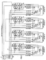
- Figure 1 represents a block diagram of a synchronous switching system incorporating the synchronization circuit according to the subject invention.
- the data to be exchanged are processed in data processing devices such as 10, 12, 14 and 16.
- a switching system 18 selects pairs of devices to be connected in order a source device can send data to a target device.
- the data are provided by each device 10, 12, 14 and 16 through data-out busses 20, 22, 24 and 26, respectively.
- Each device 10, 12, 14 and 16 receives data through switching system and data in busses 30, 32, 34 and 36 respectively.
- data means any type of binary coded information. Also, only four devices have been represented for the sake of illustration, but any number of devices can be used.
- the switching system can use any type of switching algorithm.
- the data bits are sent on the data in busses 30, 32, 34 and 36 in synchronism with a general system clock signal CO generated by a clock circuit 38 on line 40.
- This clock signal is distributed to each device through lines 40-10, 40-12, 40-14 and 40-16.
- the data bits are arranged into frames delimited by the pulses of a frame synchronization signal.
- the frame synchronization signal FO provided to the devices 10, 12, 14 and 16 is derived from the clock signal CO by counter 42 so that each frame comprises a fixed integer number of bits.
- Each data processing device 10, 12, 14 and 16 comprises a timing circuit 50, 52, 54 and 56, wich respectively generates the device clock signal CS on lines 58-10, 58-12, 58-14 and 58-16 and the device frame synchronization signal FS on lines 60-10, 60-12, 60-14 and 60-16 from the clock signal CO and the frame synchronization signal FO received from line 40 and 44.
- the clock signal CS has the same frequency as the clock signal CO, their phase differences result from the distance between the switching system and the data processing devices.
- the frame synchronization signal FS has the same frequency as signal FO but is advanced with respect to frame synchronization signal FO through counters 62-10, 62-12, 62-14 and 62-16 in order to anticipate the delay taken in the data upstream from the adapter to the switch.
- circuits 70, 72, 74 and 76 which receive the data from data-out busses 20, 22, 24 and 26 respectively, the clock signals CS and CO, the frame synchronization signals FS and FO to provide on their output busses 80, 82, 84 and 86 the resynchronized data at the input of the switching system 18.
- circuits 70, 72, 74 and 76 comprise two stages referenced as 70-1 and 70-2, 72-1 and 72-2, 74-1 and 74-2 and 76-1 and 76-2 respectively, the first stage processes the phase differences at the bit level and the second stage processes the phase differences at the frame level.
- FIG. 2 shows a detailed representation of the first stage 70-1 in circuit 70.
- the other stages 72-1, 74-1 and 76-1 are identical to stage 70-1.
- This first stage comprises two counters 100 and 102.
- the counters are initially set at different values through a control circuit 104.
- the counters 100 and 102 are modulo-n counter and counts the pulses of the signals CO and CS respectively.
- the initial value of the counter 100 is 0 and the initial value of the counter 102 is the integer number which is equal or higher than n/2, with n higher than 2 and preferably equal to 4.
- the initial values are set through control circuit 104 and AND gate 105 which prevents the clock pulses CS from being provided to counter 102 before a start pulse is generated by circuit 104, to establish the initial values of counter 100 and 102 as will be described later on.
- Decoding circuits 106 and 108 are responsive to the values reached by counters 100 and 102 received from busses 101 and 103 respectively, to activate one of their four output lines depending upon the counter values.
- Decoding circuit 106 has four output lines 110-1, 110-2, 110-3 and 110-4 activated when the counter values are 1, 2, 3 and 4 respectively.
- Decoding circuit 108 has four output lines 112-1, 112-2, 112-3 and 112-4 activated when the counter values are 1, 2, 3 and 4 respectively.
- Data-out bus 20 is a parallel bus able to carry m bits and comprises m lines 20-1 to 20-m. Each line 20-i (with 1 ⁇ i ⁇ m) of the bus is provided to the inputs of a four-stage cyclic buffer 114-i through AND gate arrangement 113-1 so that at each bit time of the clock signal CS, the bit on line 20-i is gated in one stage of cyclic buffer 114-i depending upon the value reached by counter 102.
- cyclic buffer 114-1 and gating arrangement 113-1, 119-1, 120-1 for data-out line 20-1 are shown.
- Each stage of cyclic buffer 114-1 has an output line 116-1, 116-2 116-3 and 116-4, each one being provided to one input of an AND gate 118-1, 118-2, 118-3 and 118-4 in AND gate arrangement 119-1
- AND gate 118-1 is conditioned by an active signal on output line 110-1 of decoding circuit 106
- AND gate 118-2 is conditioned by an active signal on output line 110-2
- AND gate 118-3 is conditioned by an active signal on output line 110-3
- AND gate 118-4 is conditioned by an active signal on output line 110-4.
- the output lines of the four AND gates 118-1 to 118-4 are provided to the inputs of OR gate 120-1, the output line of which constitutes one line 21-1 among the m data out lines 21-1 to 21-m which are provided to the frame synchronization part 70-2.
- the counter 102 and decoding circuit 108 allow the data bits received on line 20-1 in synchronism with the clock signal CS to be arranged sequentially in one stage of the cyclic buffer in accordance with the value reached by the counter.
- the counter 100 and decoding circuit 106 allow the data bits stored in cyclic buffer to be gated on line 21-1 in synchronism with the system clock signal CO, as explained in the table below.
- the counters 100 and 102, decoding circuits 106 and 108 and control circuit 104 are common for the control of the cyclic buffers 114-1 to 114-m and 114-FS.
- Control circuit 104 is responsive to the counter values at the outputs of decode circuits 106 and 108 to generate on its output line 122 a START/STOP signal which is provided to one input of AND gate 105 to prevent the clock signal CS from being applied to the counter as long as a start condition is not set.
- the only possible start conditions are the following:
- control circuit 104 comprises a compare circuit made of AND gates 130, 132, 134 and 136.
- AND gate 100 is connected to lines 110-1 and 112-3 and thus provides an active signal on its output line 131 when the values in counters 100 and 102 are 1 and 3 simultaneously.
- AND gate 132 is connected to lines 110-2 and 112-4 and thus provides an active signal on its output line 133 when the values in counters 100 and 102 are 2 and 4 simultaneously.
- AND gate 134 is connected to lines 110-3 and 112-1 and thus provides an active signal on its output line 135 when the values in counters 100 and 102 are 3 and 1 simultaneously.
- AND gate 136 is connected to lines 110-4 and 112-2 and thus provides an active signal on its output line 137 when the values in counters 100 and 102 are 4 and 2 simultaneously.
- the output lines 131, 133, 135 and 137 are provided to the inputs of OR gate 140 the output line of which is provided to the set input of latch 142.
- Line 141 is provided to inverter 144, the output line 145 of which is provided to the reset input of latch 142.
- the output line 122 is activated when latch 142 is set. i.e when a START condition exists.
- the clock signal CS is not provided to counter 102 before counter 100 reaches a value which favorably compares with the value in counter 102.
- the frame synchronization part 70-2 of circuit 70 is shown in Figure 4.
- the output lines 21-1 to 21-m from part 70-1 are provided to a shift register arrangement 150.
- the shift register arrangement 150 comprises m shift registers 151-1 to 151-m having p stages.
- p is chosen as a function of the largest phase difference between frame synchronization signals FO and FS.
- p is chosen equal to 3.
- Each stage is referenced by the reference number 151 followed by a suffix indicating the shift register number and the stage number, for example 151 m-2 references the second stage of shift register 151-m.
- Each data line 21-1 to 21-m is provided to the input of a shift register 151-1 to 151-m respectively, so that the data bits resynchronized with the clock signal CO are shifted in the shift registers 151-1 to 151-m under control of the clock signal CO.
- the data bits from line 21-1 to 21-m and the delayed data bits from outputs 152, 153 and 154 of each stage of shift registers 151-1 to 151-m are provided to a multiplex arrangement 156 which gates the data bits from a selected bus 21, 152, 153 or 154 onto bus 80 under control of a gating signal on one line 158, 159, 160 or 161 respectively.
- the gating control signals are generated from the resynchronized FSR signal from line 61-10 through control circuit 162.
- Signal FSR on line 61-10 is provided to the input of first stage 164-1.
- Line 61-10 and the output lines 166, 167 , 168 and each stage 164-1, 164-2 and 164-3 are provided to first inputs of AND gates 169, 170, 171 and 172 respectively.
- the second inputs of these AND gates are connected to line 44-10, so that they receive the frame synchronization signal FO. Since the signal FSR is resynchronized at the bit level, as shown in the timing diagram of Figure 5, one gate among AND gates 169 to 172 detects a coincidence between the synchronization pulse of signal FO and either the resynchronized pulse of signal FSR on line 61-10 or the delayed pulses on line 166, 167 or 168.
- latches 173 to 176 are reset at the beginning of each frame period and then only one latch is set during the frame period depending upon which AND gate 169 to 172 detects a coincidence.
- AND gate 170 detects the coincidence and latch 174 is set and generates an active gating signal on its output line 159 to gate the delayed data bits on bus 152 to bus 80.
- latch 174 is reset and the gating signal is generated by one latch among latches 173 to 176 depending upon which AND gates 169 to 172 detects the coincidence.
- the data bits on bus 80 are resynchronized at the bit level and frame level and can be switched on a selected one data-in bus 30, 32, 34 or 36.
Claims (5)
- Un circuit de synchronisation recevant des bits de données sur une liaison d'entrée (20-1) à la fréquence des impulsions d'un premier signal d'horloge (CS) dans des trames délimitées par les impulsions d'un premier signal de synchronisation de trames dérivé du premier signal d'horloge, pour délivrer lesdits bits de données sur une première ligne de sortie (80) à la fréquence d'un second signal d'horloge (CO) dans des trames délimitées par les' impulsions d'un second signal de synchronisation de trames qui a la même fréquence que le premier signal de synchronisation de trames mais n'a aucune relation de phase avec ledit premier signal de synchronisation, comprenant:- un premier moyen de comptage (102) qui compte modulo-n les impulsions du premier signal d'horloge, n étant un nombre entier au moins égal à 2,- un second moyen de comptage (100) qui compte modulo-n les impulsions du second signal d'horloge,- un premier moyen de mise en mémoire intermédiaire (114-1) comprenant n étages,- des premiers moyens de transfert (113-1) sensibles aux valeurs atteintes par le premier moyen de comptage pour transférer et emmagasiner cycliquement les bits reçus dans les étages du premier moyen de mise en mémoire intermédiaire dans une première séquence prédéterminée, le numéro de l'étage dans lequel un bit reçu est transféré, étant déterminé par une première relation établie entre les numéros des étages et les valeurs atteintes par le premier moyen de comptage,- des seconds moyens de transfert (119-1, 120-1) sensibles aux valeurs atteintes par le second moyen de comptage pour transférer cycliquement les bits emmagasinés dans les étages du premier moyen de mise en mémoire intermédiaire, sur une seconde ligne de sortie (21-1) dans une seconde séquence prédéterminée, le numéro de l'étage depuis lequel un bit est transféré sur la seconde ligne de sortie, étant déterminé par une seconde relation entre les numéros des étages et les valeurs atteintes par le second moyen de comptage, si bien que les bits sont délivrés sur la première ligne de sortie à la fréquence des impulsions du second signal d'horloge dans le même ordre que celui de leur réception,- ledit circuit de synchronisation étant en outre caractérisé en ce que les premier et second moyens de comptage sont initialement conditionnés à une première et à une seconde valeur initiale, respectivement, la seconde valeur initiale étant différente de la première et étant caractérisé en ce qu'il comprend:- un second moyen de mise en mémoire intermédiaire (114-FS) comprenant n étages,- des troisièmes moyens de transfert (113-FS) sensibles aux valeurs atteintes par le premier moyen de comptage pour transférer les impulsions du premier signal de synchronisation de trames dans les étages de la seconde mémoire intermédiaire déterminés par la première relation,- des quatrièmes moyens de transfert (119-FS, 120-FS) sensibles aux valeurs atteintes par le second moyen de comptage pour transférer les impulsions emmagasinées dans les étages du second moyen de mise en mémoire intermédiaire, déterminés par la seconde relation et délivrant ainsi un signal de trames resynchronisées sur une ligne de trames resynchronisées (61-10),- un circuit de resynchronisation de trames (150-152) connecté à la ligne de trames resynchronisées et à la seconde ligne de sortie et sensible au second signal de resynchronisation de trames pour aligner les bits de données issus de la seconde ligne de sortie avec les secondes impulsions de synchronisation de trames et pour délivrer les bits de données ainsi alignés sur la première ligne de sortie (80).
- Un circuit de synchronisation selon la revendication 1, caractérisé en ce que les premier et second moyens de comptage sont initialement conditionnés à des valeurs qui diffèrent d'un nombre entier x qui est égal ou supérieur à n/2.
- Un circuit de synchronisation selon la revendication 2, caractérisé en ce que n est égal à 4.
- Un circuit de synchronisation selon la revendication 2 ou 3, caractérisé en ce que les première et seconde relations sont identiques.
- Un circuit de synchronisation selon l'une quelconque des revendications 1 à 4, caractérisé en ce que le circuit de resynchronisation de trames comprend:- un premier registre à décalage de p étages (151-1) dans lequel les bits de données issus de la seconde ligne de sortie (21-1) sont appliqués en entrée et décalés sous la commande du second signal d'horloge (CO), p étant un nombre entier supérieur à 2,- un second registre à décalage de p étages (164) dans lequel le signal de trames resynchronisées est appliqué en entrée et décalé sous la commande du second signal d'horloge,- des moyens de mesure (169) sensibles au second signal de synchronisation de trames et au signal de trames resynchronisées à l'entrée du second registre à décalage et au signal de resynchronisation de trames retardé à la sortie de chaque étage du second registre à décalage pour mesurer le nombre des impulsions d'horloge du second signal d'horloge séparant la seconde impulsion de synchronisation de trames et l'impulsion de trames resynchronisées, au début de chaque trame,- des cinquièmes moyens de transfert (156) sensibles à la mesure exécutée par le moyen de mesure pour transférer les bits de données de la seconde ligne de sortie ou les bits de données retardés à une sortie d'un étage sélectionné du premier registre à décalage, sur la première ligne de sortie suivant le nombre mesuré d'impulsions d'horloge.
Priority Applications (4)
| Application Number | Priority Date | Filing Date | Title |
|---|---|---|---|
| EP90480046A EP0447731B1 (fr) | 1990-03-13 | 1990-03-13 | Dispositif de synchronisation pour un système de commutation synchrone |
| DE69022025T DE69022025T2 (de) | 1990-03-13 | 1990-03-13 | Synchronisierungsschaltung für ein synchrones Vermittlungssystem. |
| JP3041050A JPH0793615B2 (ja) | 1990-03-13 | 1991-02-13 | 同期化回路 |
| US07/657,906 US5134636A (en) | 1990-03-13 | 1991-02-20 | Synchronization circuit for a synchronous switching system |
Applications Claiming Priority (1)
| Application Number | Priority Date | Filing Date | Title |
|---|---|---|---|
| EP90480046A EP0447731B1 (fr) | 1990-03-13 | 1990-03-13 | Dispositif de synchronisation pour un système de commutation synchrone |
Publications (2)
| Publication Number | Publication Date |
|---|---|
| EP0447731A1 EP0447731A1 (fr) | 1991-09-25 |
| EP0447731B1 true EP0447731B1 (fr) | 1995-08-30 |
Family
ID=8205829
Family Applications (1)
| Application Number | Title | Priority Date | Filing Date |
|---|---|---|---|
| EP90480046A Expired - Lifetime EP0447731B1 (fr) | 1990-03-13 | 1990-03-13 | Dispositif de synchronisation pour un système de commutation synchrone |
Country Status (4)
| Country | Link |
|---|---|
| US (1) | US5134636A (fr) |
| EP (1) | EP0447731B1 (fr) |
| JP (1) | JPH0793615B2 (fr) |
| DE (1) | DE69022025T2 (fr) |
Families Citing this family (7)
| Publication number | Priority date | Publication date | Assignee | Title |
|---|---|---|---|---|
| EP0499762A1 (fr) * | 1991-02-21 | 1992-08-26 | International Business Machines Corporation | Dispositif de synchronisation pour effectuer des fonctions de commutation synchrone de circuits dans un noeud asynchrone de communication |
| US5537418A (en) * | 1993-03-11 | 1996-07-16 | Unisys Corporation | Data transmit resynchronization at a node |
| JP3233801B2 (ja) * | 1994-12-09 | 2001-12-04 | 沖電気工業株式会社 | ビット位相同期回路 |
| US5923710A (en) * | 1997-02-05 | 1999-07-13 | Tektronix, Inc. | Synchronous switching of digital audio while maintaining block alignment |
| US6466626B1 (en) | 1999-02-23 | 2002-10-15 | International Business Machines Corporation | Driver with in-situ variable compensation for cable attenuation |
| KR100784594B1 (ko) * | 2006-11-28 | 2007-12-11 | 엘지노텔 주식회사 | 시간 도메인에서의 파워 측정값을 이용한 tdd 프레임동기 획득 방법 및 시스템 |
| US7863931B1 (en) * | 2007-11-14 | 2011-01-04 | Lattice Semiconductor Corporation | Flexible delay cell architecture |
Family Cites Families (8)
| Publication number | Priority date | Publication date | Assignee | Title |
|---|---|---|---|---|
| GB1195899A (en) * | 1967-11-21 | 1970-06-24 | Mini Of Technology | Improvements in or relating to Synchronising Arrangements in Digital Communications Systems. |
| JPS55127745A (en) * | 1979-03-26 | 1980-10-02 | Hitachi Denshi Ltd | Bit buffer system |
| US4763339A (en) * | 1984-03-15 | 1988-08-09 | General Electric Company | Digital word synchronizing arrangement |
| JPS62279748A (ja) * | 1986-05-29 | 1987-12-04 | Nec Corp | ビツトバツフア回路 |
| JPH0828691B2 (ja) * | 1988-03-14 | 1996-03-21 | 富士通株式会社 | フレーム同期方式 |
| FR2631762B1 (fr) * | 1988-05-18 | 1991-02-15 | Cit Alcatel | Dispositif de synchronisation de trame pour un train numerique synchrone partage en blocs au moyen d'un code par blocs et structure en trames |
| FR2635624B1 (fr) * | 1988-08-19 | 1994-05-13 | Abiven Jacques | Procede de synchronisation et dispositifs de recuperation de synchronisation pour communications a l'alternat |
| JPH02234529A (ja) * | 1989-03-08 | 1990-09-17 | Fujitsu Ltd | フレームアライナ回路 |
-
1990
- 1990-03-13 EP EP90480046A patent/EP0447731B1/fr not_active Expired - Lifetime
- 1990-03-13 DE DE69022025T patent/DE69022025T2/de not_active Expired - Fee Related
-
1991
- 1991-02-13 JP JP3041050A patent/JPH0793615B2/ja not_active Expired - Fee Related
- 1991-02-20 US US07/657,906 patent/US5134636A/en not_active Expired - Lifetime
Also Published As
| Publication number | Publication date |
|---|---|
| JPH0793615B2 (ja) | 1995-10-09 |
| DE69022025D1 (de) | 1995-10-05 |
| JPH0568026A (ja) | 1993-03-19 |
| EP0447731A1 (fr) | 1991-09-25 |
| US5134636A (en) | 1992-07-28 |
| DE69022025T2 (de) | 1996-04-18 |
Similar Documents
| Publication | Publication Date | Title |
|---|---|---|
| US5568526A (en) | Self timed interface | |
| JP2747077B2 (ja) | フレーム同期回路 | |
| US4119796A (en) | Automatic data synchronizer | |
| US4881165A (en) | Method and apparatus for high speed data transmission between two systems operating under the same clock with unknown and non constant skew in the clock between the two systems | |
| CA1298420C (fr) | Systeme demultiplexeur | |
| US5058132A (en) | Clock distribution system and technique | |
| US4811364A (en) | Method and apparatus for stabilized data transmission | |
| JPH03113928A (ja) | クロック同期ネットワーク及びデータ通信法 | |
| JPH08163116A (ja) | フレーム同期装置 | |
| EP0447731B1 (fr) | Dispositif de synchronisation pour un système de commutation synchrone | |
| US6185693B1 (en) | Synchronous interface for transmitting data in a system of massively parallel processors | |
| EP0312260A2 (fr) | Circuit de démultiplexage à grande vitesse | |
| US5485298A (en) | Optical packet synchronization circuit | |
| EP0004887A1 (fr) | Méthode et dispositif pour la synchronisation de transmissions numériques par satellite | |
| US4394758A (en) | Synchronizing unit for receiving section of PCM station | |
| US6023768A (en) | Phase locked distributed time reference for digital processing and method therefor | |
| EP0520127A1 (fr) | Circuit numérique de synchronisation utilisant une ligne de rétard accordée et branchée | |
| US5781587A (en) | Clock extraction circuit | |
| KR100204062B1 (ko) | 저속 데이타 프레임 위상 정렬기 | |
| JPH05336091A (ja) | バス通信システム | |
| JPH05235976A (ja) | 通信スイッチ | |
| JPH0834457B2 (ja) | 同期式伝送システムの受信カウンタ位相同期回路 | |
| US4095048A (en) | Method of synchronizing a pulse code modulation (pcm) junction and an arrangement for applying this method | |
| KR920006791B1 (ko) | 리프레임시 버퍼의 딜레이를 제거한 독립 동기 구성회로 | |
| KR0126860B1 (ko) | 대용량 비동기 송수신기 정합(g-taxi) 수신 장치 |
Legal Events
| Date | Code | Title | Description |
|---|---|---|---|
| PUAI | Public reference made under article 153(3) epc to a published international application that has entered the european phase |
Free format text: ORIGINAL CODE: 0009012 |
|
| AK | Designated contracting states |
Kind code of ref document: A1 Designated state(s): DE FR GB |
|
| 17P | Request for examination filed |
Effective date: 19911219 |
|
| 17Q | First examination report despatched |
Effective date: 19931018 |
|
| GRAA | (expected) grant |
Free format text: ORIGINAL CODE: 0009210 |
|
| AK | Designated contracting states |
Kind code of ref document: B1 Designated state(s): DE FR GB |
|
| REF | Corresponds to: |
Ref document number: 69022025 Country of ref document: DE Date of ref document: 19951005 |
|
| ET | Fr: translation filed | ||
| PGFP | Annual fee paid to national office [announced via postgrant information from national office to epo] |
Ref country code: FR Payment date: 19960307 Year of fee payment: 7 |
|
| PLBE | No opposition filed within time limit |
Free format text: ORIGINAL CODE: 0009261 |
|
| STAA | Information on the status of an ep patent application or granted ep patent |
Free format text: STATUS: NO OPPOSITION FILED WITHIN TIME LIMIT |
|
| 26N | No opposition filed | ||
| PG25 | Lapsed in a contracting state [announced via postgrant information from national office to epo] |
Ref country code: FR Free format text: LAPSE BECAUSE OF NON-PAYMENT OF DUE FEES Effective date: 19971128 |
|
| REG | Reference to a national code |
Ref country code: FR Ref legal event code: ST |
|
| PGFP | Annual fee paid to national office [announced via postgrant information from national office to epo] |
Ref country code: GB Payment date: 20000301 Year of fee payment: 11 |
|
| PGFP | Annual fee paid to national office [announced via postgrant information from national office to epo] |
Ref country code: DE Payment date: 20000420 Year of fee payment: 11 |
|
| PG25 | Lapsed in a contracting state [announced via postgrant information from national office to epo] |
Ref country code: GB Free format text: LAPSE BECAUSE OF NON-PAYMENT OF DUE FEES Effective date: 20010313 |
|
| GBPC | Gb: european patent ceased through non-payment of renewal fee |
Effective date: 20010313 |
|
| PG25 | Lapsed in a contracting state [announced via postgrant information from national office to epo] |
Ref country code: DE Free format text: LAPSE BECAUSE OF NON-PAYMENT OF DUE FEES Effective date: 20020101 |