EP0447650A2 - Circuit intégrable pour traiter des signaux logiques - Google Patents
Circuit intégrable pour traiter des signaux logiques Download PDFInfo
- Publication number
- EP0447650A2 EP0447650A2 EP90124628A EP90124628A EP0447650A2 EP 0447650 A2 EP0447650 A2 EP 0447650A2 EP 90124628 A EP90124628 A EP 90124628A EP 90124628 A EP90124628 A EP 90124628A EP 0447650 A2 EP0447650 A2 EP 0447650A2
- Authority
- EP
- European Patent Office
- Prior art keywords
- connection
- transistor
- transistors
- gate
- mos switching
- Prior art date
- Legal status (The legal status is an assumption and is not a legal conclusion. Google has not performed a legal analysis and makes no representation as to the accuracy of the status listed.)
- Pending
Links
Images

Classifications
-
- H—ELECTRICITY
- H03—ELECTRONIC CIRCUITRY
- H03K—PULSE TECHNIQUE
- H03K19/00—Logic circuits, i.e. having at least two inputs acting on one output; Inverting circuits
- H03K19/02—Logic circuits, i.e. having at least two inputs acting on one output; Inverting circuits using specified components
- H03K19/08—Logic circuits, i.e. having at least two inputs acting on one output; Inverting circuits using specified components using semiconductor devices
- H03K19/094—Logic circuits, i.e. having at least two inputs acting on one output; Inverting circuits using specified components using semiconductor devices using field-effect transistors
- H03K19/0944—Logic circuits, i.e. having at least two inputs acting on one output; Inverting circuits using specified components using semiconductor devices using field-effect transistors using MOSFET or insulated gate field-effect transistors, i.e. IGFET
- H03K19/09448—Logic circuits, i.e. having at least two inputs acting on one output; Inverting circuits using specified components using semiconductor devices using field-effect transistors using MOSFET or insulated gate field-effect transistors, i.e. IGFET in combination with bipolar transistors [BIMOS]
-
- H—ELECTRICITY
- H03—ELECTRONIC CIRCUITRY
- H03K—PULSE TECHNIQUE
- H03K3/00—Circuits for generating electric pulses; Monostable, bistable or multistable circuits
- H03K3/02—Generators characterised by the type of circuit or by the means used for producing pulses
- H03K3/021—Generators characterised by the type of circuit or by the means used for producing pulses by the use, as active elements, of more than one type of element or means, e.g. BIMOS, composite devices such as IGBT
-
- H—ELECTRICITY
- H03—ELECTRONIC CIRCUITRY
- H03K—PULSE TECHNIQUE
- H03K3/00—Circuits for generating electric pulses; Monostable, bistable or multistable circuits
- H03K3/02—Generators characterised by the type of circuit or by the means used for producing pulses
- H03K3/26—Generators characterised by the type of circuit or by the means used for producing pulses by the use, as active elements, of bipolar transistors with internal or external positive feedback
- H03K3/28—Generators characterised by the type of circuit or by the means used for producing pulses by the use, as active elements, of bipolar transistors with internal or external positive feedback using means other than a transformer for feedback
- H03K3/281—Generators characterised by the type of circuit or by the means used for producing pulses by the use, as active elements, of bipolar transistors with internal or external positive feedback using means other than a transformer for feedback using at least two transistors so coupled that the input of one is derived from the output of another, e.g. multivibrator
- H03K3/286—Generators characterised by the type of circuit or by the means used for producing pulses by the use, as active elements, of bipolar transistors with internal or external positive feedback using means other than a transformer for feedback using at least two transistors so coupled that the input of one is derived from the output of another, e.g. multivibrator bistable
- H03K3/288—Generators characterised by the type of circuit or by the means used for producing pulses by the use, as active elements, of bipolar transistors with internal or external positive feedback using means other than a transformer for feedback using at least two transistors so coupled that the input of one is derived from the output of another, e.g. multivibrator bistable using additional transistors in the input circuit
- H03K3/2885—Generators characterised by the type of circuit or by the means used for producing pulses by the use, as active elements, of bipolar transistors with internal or external positive feedback using means other than a transformer for feedback using at least two transistors so coupled that the input of one is derived from the output of another, e.g. multivibrator bistable using additional transistors in the input circuit the input circuit having a differential configuration
Definitions
- the invention consists of an integrable circuit for processing logic signals according to the preamble of claim 1.
- the number of switching elements that can be integrated on a chip has always increased due to the refinement of the chip structures. For example, at the beginning of the implementation phase of integrated circuits, it was still possible to route all inputs and outputs of a gate circuit integrated on a module to the outside via a connection pin, so this is possible with highly integrated circuits due to a limited number of connection pins no more. The consequence of this would be that the circuits integrated on a chip can no longer be checked and thus a detailed error detection would no longer be possible. In order to remedy this problem, one uses test circuit logic which is accommodated on the chip together with the circuit which implements the desired function.
- test circuit logic With the help of this test circuit logic, it is possible to check the relevant gate inputs and outputs already on the chip and only to deliver the result of such a check to the outside via a connecting pin.
- Checks of the circuit logic are generally not part of the regular functional sequence of the user circuit. Test circuits are only active at certain times, for example when they are switched on, which means that the requirements regarding speed may not be as high as the requirements for the useful circuit in this regard. High switching speeds can be achieved with the known one Circuit technology only through high permanent power consumption. This power consumption results in a high power loss, strong component heating and, to counteract this, one expensive cooling equipment. If there is an opportunity to reduce this high power loss, it is advantageous to use this option. In the case of the test logic integrated on a chip, a power saving is particularly advantageous since the proportion of the test logic circuits in the number of the total circuits integrated on a chip is 10 to 15%.
- the current consumption of the circuit is determined solely by the current source. Halving, for example, the current intensity supplied by the power source by half also reduces the power loss by half.
- the outputs of the circuit are located in the two current branches between the load resistors and the main current paths of the switching transistors. The two possible logic states are generated by blocking or making the main current path of a switching transistor. In the ideal case - unloaded output - no current flows through the load resistor when the main transistor current path is blocked. The level of the second constant supply voltage is present at the output.
- the current determined by the current source flows through the main current path of the switching transistor and through the load resistor.
- a voltage drops across the load resistor which corresponds to the difference level between the two logic states at the output.
- This difference level hereinafter referred to as the stroke, must not fall below 95% of its maximum value if it is to be able to be evaluated well and reliably. Deviating from the ideal state, however, a current which is smaller by the current amplification factor B than in the main current path of the input switching transistor of this downstream logic circuit flows into the control input of a logic circuit downstream of the circuit under consideration.
- the condition follows that the current in the main current path of the downstream logic circuit divided by the current amplification factor B must be less than 5% of that current which flows in the main current path of the circuit under consideration. Realizable values of the current amplification factor are around 50. By inserting this value in the aforementioned condition, it follows that the current in the main current path of the circuit under consideration must be at least 0.4 times as large as the current in the main current path of the downstream logic circuit. If several interconnected logic circuits work with the same current in the main current path, then up to three inputs of a logic circuit can be connected to one output.
- the object on which the present invention is based is to create a possibility for power reduction which does not simultaneously result in a reduction in the FAN-OUT.
- the usual working resistances in the current branches are exchanged for collector-emitter sections of pnp bipolar transistors. While the current-voltage characteristic of an ohmic resistor has a linear profile - the resistance value is always constant - the collector current rises sharply with a low collector-emitter voltage so that it hardly changes at higher collector-emitter voltages. So if the pnp bipolar transistor is conductive, it shows a low resistance, if it blocks, it has a very large resistance value. With the help of this pnp bipolar transistor used as a load resistor, it is possible, depending on the respective requirement, to change the value of this load resistor.
- the transistor main current path If the drain-source path of a MOS switching transistor, referred to as the transistor main current path, is conductive, then a large load resistor with a low current ensures a sufficiently large stroke of the output level, whereas, when the drain-source path of the MOS switching transistor is blocked, a low-resistance load resistor itself ensures with a relatively low-impedance output load, a small voltage drop.
- the target-specific change in the load resistance is achieved by connecting the base connections of the pnp bipolar transistors to the respective other current branch.
- the present circuit which can also be regarded as a differential amplifier, only one of the two drain-source paths of the MOS switching transistors is always conductive, while the other is blocking. Complementary output states are always present at the drain connections of the two MOS switching transistors which form the logic outputs of the circuit. If the first switching transistor blocks, then its drain connection is approximately the second constant supply voltage.
- the pnp bipolar transistor, the collector-emitter path of which forms the load resistor for the current branch in which the second MOS switching transistor is located, is blocked and thus has a high resistance since its base is connected to the drain of the first MOS switching transistor.
- the collector-emitter path of which is located in the same current branch as the first MOS switching transistor, there is a relatively low potential - low level. This low potential makes the pnp bipolar transistor conductive or low-resistance.
- This slow and energy-saving circuit can be used in combination with the 100% faster current switch logic in pure bipolar technology.
- the high-impedance input resistance of the first MOS switching transistor hardly loads the output of a preceding switching stage, so that it does not interfere with the fast switching processes during normal operation of the integrated circuit.
- the circuit can drive a large number of downstream switching stages using pure bipolar technology.
- the current amplification of the pnp bipolar transistors has a disadvantageous effect, since it leads to different current intensities in the two current branches of the circuit. These different currents cause a hysteresis of the switching threshold of the logic circuit.
- the second MOS switching transistor at the drain connection of which there is a low level (-0.8 V) can only be blocked at a voltage of -0.1 V at the gate connection of the first MOS switching transistor, that is to say into the high state ( OV) switch, whereas this second MOS switching transistor can only be switched back to the conductive state when -0.4 volts are applied to the gate connection of the first MOS switching transistor.
- the emitter area ratio of the two pnp bipolar transistors interconnected to form a current mirror is known to determine the total current gain largely independently of the individual current gains of the transistors involved.
- the setting of certain emitter area ratios is technologically manageable.
- the desired hysteresis can thus be set during the manufacturing process of the circuit or the hysteresis can be completely eliminated.
- the basic function of the logic circuit is expanded to an OR / NOR function by connecting the drain-source path of a further MOS switching transistor, which also serves as a gate input, to the drain-source path of the MOS switching transistor serving as a gate input.
- this is achieved by connecting one or more main current paths from transistors in parallel to the main current path of the input switching transistor.
- series gating is a serial logical link, in which the power switches are arranged one above the other in series and are fed together from a power source.
- series gating is a serial logical link, in which the power switches are arranged one above the other in series and are fed together from a power source.
- the logic voltage and reference voltage levels coming from the outside have to be shifted as required for the individual current switches connected in series by level adjustment circuits.
- This level shift can be eliminated by using MOS switching transistors, since its current-voltage characteristic can be influenced by varying the area of a MOS transistor.
- the MOS switching transistors connected together at their source connections each form a current switch. If you change the area of the MOS switching transistors from one current switch to another and apply the same reference voltage to each of these current switches, then the absolute levels of the switching thresholds differ from current switch to current switch.
- Level shifter circuits can thus be dispensed with if this effect is used consistently, thereby achieving a further power saving effect and saving the chip area otherwise required for the level shifters.
- the provision of different reference voltage levels can also be dispensed with and a reference voltage can be applied simultaneously to a plurality of current switch transistor pairs arranged in series or in parallel.
- CML technology is a current switch technology that differs from ECL technology only in that the npn bipolar transistors in the emitter follower circuit, which are not present at the output, differ.
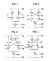
- An npn bipolar transistor TB3 serves as the current source, the emitter connection of which is connected to a constant supply voltage VEE, the base connection of which is supplied with a reference voltage VSM which controls the current intensity and whose collector connection is connected both to the emitter connection of a first npn bipolar switching transistor TB1 and to the emitter connection of a second npn -Bipolar transistor TB2 is connected.
- the collector connections of the two npn bipolar switching transistors TB1, TB2 serve as mutually complementary outputs Q, Q the inverter circuit and are each connected via a load resistor R1, R2 to a second constant supply voltage VCC, which is positive with respect to the first constant supply voltage VEE.
- the switching threshold of the inverter is determined with the aid of a second reference voltage which is present at the base connection of the second npn bipolar switching transistor TB2.
- the inverter input E forms the base connection of the first npn bipolar switching transistor TB1.
- MOS transistors shown in this and in the following figures are so-called self-blocking n-MOS transistors.
- a MOS transistor T3 has its source connected to the supply voltage VEE. This MOS transistor is used as a current source and is controlled by the reference voltage VSM at its gate connection.
- the drain connection is connected to the source connections of two MOS switching transistors T1, T2.
- the drain connection of the first MOS switching transistor T1 is connected to the collector connection of a pnp bipolar transistor T4 and to the base connection of a second pnp bipolar transistor T5, and the drain connection of the second MOS switching transistor T2 is connected to the collector connection of the second pnp bipolar transistor T5 and to the Base terminal of the first pnp bipolar transistor T4 connected.
- the emitters of the two pnp bipolar transistors T4, T5 are supplied by the second constant supply voltage VCC.
- the second reference voltage VB1 At the gate terminal of the second MOS switching transistor T2 is the second reference voltage VB1, with which, as in FIG. 1, the switching threshold of the inverter is set.
- the gate connection of the MOS switching transistor T1 forms the input E of the inverter.
- a third and a fourth pnp bipolar transistor T6, T7 are additionally inserted into the circuit.
- the base and collector terminal of the third pnp bipolar transistor T6 is connected to the base of the first pnp bipolar transistor T4 and the base terminal and the collector terminal of the fourth pnp bipolar transistor T7 is connected to the base terminal of the second pnp bipolar transistor T5.
- the emitter connections of the additionally inserted pnp bipolar transistors T6, T7 are connected to the second constant supply voltage VCC.
- the first and third pnp bipolar transistors T4, T6 and the second and fourth pnp bipolar transistors T5, T7 each form a current mirror.
- a MOS switching transistor T11 is shown in addition to the circuit shown in FIG. 2, in addition to the circuit shown in FIG. 2, a MOS switching transistor T11 is shown. Both its drain and its source connection are connected to the corresponding connection of the first MOS switching transistor T1. The gate terminal of the MOS switching transistor T11 additionally inserted into the circuit forms a second gate input E1. The inputs E and E1 form with respect to the gate outputs Q and Q the inputs of an OR or NOR gate.
- FIG. 5 shows an AND or NAND gate with the input E and an input E2 and the outputs Q and Q .
- the drain-source path of a third MOS switching transistor T8 is inserted.
- This MOS switching transistor T8 forms, together with a fourth MOS switching transistor T9, whose source connection is connected to the source connection of the third MOS switching transistor T8, a second current switch which is arranged in series with the first current switch formed from the two MOS switching transistors T1, T2 is. Because of this series connection, this circuit variant is also referred to as a "series gating circuit".
- the switching threshold of the second current switch is determined by connecting the gate terminal of the fourth MOS switching transistor T9 to the second reference voltage VB1.
- the drain of the fourth MOS switching transistor T9 is connected to the output Q.
- the two current switches connected in series switch despite setting the switching threshold by means of a single reference voltage VB1 at different absolute voltage levels. This is possible because the MOS switching transistors T8, T9 and T1, T2 on the semiconductor chip take up different sized geometric areas.
- p-channel MOS switching transistors and npn bipolar transistors can also be used in an equally advantageous manner if the operating voltages are reversed.
Landscapes
- Engineering & Computer Science (AREA)
- Power Engineering (AREA)
- Logic Circuits (AREA)
- Physics & Mathematics (AREA)
- Computer Hardware Design (AREA)
- Computing Systems (AREA)
- General Engineering & Computer Science (AREA)
- Mathematical Physics (AREA)
Applications Claiming Priority (2)
| Application Number | Priority Date | Filing Date | Title |
|---|---|---|---|
| DE4005035 | 1990-02-16 | ||
| DE19904005035 DE4005035C1 (fr) | 1990-02-16 | 1990-02-16 |
Publications (2)
| Publication Number | Publication Date |
|---|---|
| EP0447650A2 true EP0447650A2 (fr) | 1991-09-25 |
| EP0447650A3 EP0447650A3 (en) | 1991-12-27 |
Family
ID=6400405
Family Applications (1)
| Application Number | Title | Priority Date | Filing Date |
|---|---|---|---|
| EP19900124628 Pending EP0447650A3 (en) | 1990-02-16 | 1990-12-18 | Integratable circuit for processing logic signals |
Country Status (4)
| Country | Link |
|---|---|
| EP (1) | EP0447650A3 (fr) |
| JP (1) | JPH07131334A (fr) |
| DE (1) | DE4005035C1 (fr) |
| IE (1) | IE910536A1 (fr) |
Family Cites Families (6)
| Publication number | Priority date | Publication date | Assignee | Title |
|---|---|---|---|---|
| JPS63164527A (ja) * | 1986-12-25 | 1988-07-07 | Matsushita Electric Ind Co Ltd | 化合物半導体集積回路 |
| JPS63250914A (ja) * | 1987-04-07 | 1988-10-18 | Yamaha Corp | エミツタ・カツプルド・ロジツク回路 |
| JPS6439117A (en) * | 1987-08-03 | 1989-02-09 | Nec Corp | Emitter-coupled logic circuit |
| GB8718654D0 (en) * | 1987-08-06 | 1987-09-09 | Plessey Co Plc | Transistor switching circuits |
| JPH088483B2 (ja) * | 1987-08-10 | 1996-01-29 | 日本電信電話株式会社 | Eclレベル出力回路 |
| JPH0191523A (ja) * | 1987-10-02 | 1989-04-11 | Nippon Telegr & Teleph Corp <Ntt> | 論理回路 |
-
1990
- 1990-02-16 DE DE19904005035 patent/DE4005035C1/de not_active Expired - Fee Related
- 1990-12-18 EP EP19900124628 patent/EP0447650A3/de active Pending
-
1991
- 1991-02-13 JP JP3041312A patent/JPH07131334A/ja not_active Withdrawn
- 1991-02-15 IE IE53691A patent/IE910536A1/en unknown
Also Published As
| Publication number | Publication date |
|---|---|
| EP0447650A3 (en) | 1991-12-27 |
| JPH07131334A (ja) | 1995-05-19 |
| DE4005035C1 (fr) | 1991-07-18 |
| IE910536A1 (en) | 1991-08-28 |
Similar Documents
| Publication | Publication Date | Title |
|---|---|---|
| EP0096944B1 (fr) | Circuit avec plusieurs chemins de signaux formés par des composants actifs | |
| DE2660843C2 (de) | Als Synchron-Binärzähler ausgebildete logische Schaltungsanordnung | |
| DE2544974B2 (de) | Schaltkreis zur Realisierung logischer Funktionen | |
| DE1762172C3 (de) | Verknüpfungsschaltung mit Stromübernahmeschaltern | |
| DE69612007T2 (de) | Ausgangspuffer mit gemeinsam genutzten zwischenknoten | |
| EP0024468B1 (fr) | Circuit à éléments de Josephson commandé par injection de courant et son utilisation dans des circuits logiques | |
| EP0416323A2 (fr) | Convertisseur de niveaux de signaux | |
| DE1537972C3 (de) | Schaltanordnung zur Verbesserung der An- und Abschalteigenschaften eines Schalttransistors einer binären Schaltung | |
| DE3587924T2 (de) | Schaltung zur Beschleunigung des Hoch-Tief-Überganges für TTL-Gatter. | |
| DE4010145C1 (fr) | ||
| DE60209621T2 (de) | Stromschaltkreis | |
| DE3878276T2 (de) | Tri-state-ausgangsschaltung. | |
| DE3009014C2 (fr) | ||
| DE2509732B2 (de) | Schaltungsanordnung zur Korrelation zweier Gruppen paralleler Binärsignale | |
| DE2518861A1 (de) | Logische stromschaltung | |
| EP0673118B1 (fr) | Convertisseur de niveau ECL en CMOS de type BiCMOS | |
| DE1537236B2 (de) | Im Takt geschalteter ein und ruck stellbarer FUp Flop | |
| DE2525690C3 (de) | Logische DOT-Verknüpfungsschaltung in Komplementär-Feldeffekttransistor-Technik | |
| DE1807105B2 (de) | Treiberschaltung für Flip-Flops | |
| DE10319089B4 (de) | Flip-Flop-Schaltungsanordnung | |
| DE3884713T2 (de) | Logische Schaltung. | |
| DE69630018T2 (de) | Logische schaltung für niedrige spannungen | |
| DE1267249B (de) | Eingangstorschaltung fuer eine bistabile Speicherschaltung | |
| EP0447650A2 (fr) | Circuit intégrable pour traiter des signaux logiques | |
| DE4030631C2 (fr) |
Legal Events
| Date | Code | Title | Description |
|---|---|---|---|
| PUAI | Public reference made under article 153(3) epc to a published international application that has entered the european phase |
Free format text: ORIGINAL CODE: 0009012 |
|
| 17P | Request for examination filed |
Effective date: 19901218 |
|
| AK | Designated contracting states |
Kind code of ref document: A2 Designated state(s): DE FR GB IT NL |
|
| PUAL | Search report despatched |
Free format text: ORIGINAL CODE: 0009013 |
|
| AK | Designated contracting states |
Kind code of ref document: A3 Designated state(s): DE FR GB IT NL |
|
| 18D | Application deemed to be withdrawn |
Effective date: 19920507 |
|
| D18D | Application deemed to be withdrawn (deleted) | ||
| STAA | Information on the status of an ep patent application or granted ep patent |
Free format text: STATUS: THE APPLICATION IS DEEMED TO BE WITHDRAWN |
|
| R18D | Application deemed to be withdrawn (corrected) |
Effective date: 19920630 |