EP0446812B1 - Fotodetektor und Bildabtaster dafür - Google Patents
Fotodetektor und Bildabtaster dafür Download PDFInfo
- Publication number
- EP0446812B1 EP0446812B1 EP91103607A EP91103607A EP0446812B1 EP 0446812 B1 EP0446812 B1 EP 0446812B1 EP 91103607 A EP91103607 A EP 91103607A EP 91103607 A EP91103607 A EP 91103607A EP 0446812 B1 EP0446812 B1 EP 0446812B1
- Authority
- EP
- European Patent Office
- Prior art keywords
- light beam
- main
- signal
- photosensor
- light
- Prior art date
- Legal status (The legal status is an assumption and is not a legal conclusion. Google has not performed a legal analysis and makes no representation as to the accuracy of the status listed.)
- Expired - Lifetime
Links
- 239000004065 semiconductor Substances 0.000 claims description 37
- 238000006243 chemical reaction Methods 0.000 claims description 13
- 239000002131 composite material Substances 0.000 claims description 9
- 230000004044 response Effects 0.000 claims description 6
- 229910052751 metal Inorganic materials 0.000 claims description 2
- 239000002184 metal Substances 0.000 claims description 2
- 230000003287 optical effect Effects 0.000 claims description 2
- 238000005070 sampling Methods 0.000 claims 1
- 239000000758 substrate Substances 0.000 description 13
- 238000010586 diagram Methods 0.000 description 9
- 238000004519 manufacturing process Methods 0.000 description 8
- 238000000034 method Methods 0.000 description 8
- 239000000463 material Substances 0.000 description 7
- 238000003491 array Methods 0.000 description 6
- 239000011521 glass Substances 0.000 description 6
- 229910052782 aluminium Inorganic materials 0.000 description 3
- XAGFODPZIPBFFR-UHFFFAOYSA-N aluminium Chemical compound [Al] XAGFODPZIPBFFR-UHFFFAOYSA-N 0.000 description 3
- 230000008569 process Effects 0.000 description 3
- 230000010354 integration Effects 0.000 description 2
- 230000000737 periodic effect Effects 0.000 description 2
- 239000000872 buffer Substances 0.000 description 1
- 238000001514 detection method Methods 0.000 description 1
- 230000006870 function Effects 0.000 description 1
- 239000012535 impurity Substances 0.000 description 1
- 230000007246 mechanism Effects 0.000 description 1
- 238000012544 monitoring process Methods 0.000 description 1
- 230000003071 parasitic effect Effects 0.000 description 1
- 108091008695 photoreceptors Proteins 0.000 description 1
- 239000013589 supplement Substances 0.000 description 1
- 238000007740 vapor deposition Methods 0.000 description 1
Images


Classifications
-
- H—ELECTRICITY
- H04—ELECTRIC COMMUNICATION TECHNIQUE
- H04N—PICTORIAL COMMUNICATION, e.g. TELEVISION
- H04N1/00—Scanning, transmission or reproduction of documents or the like, e.g. facsimile transmission; Details thereof
- H04N1/04—Scanning arrangements, i.e. arrangements for the displacement of active reading or reproducing elements relative to the original or reproducing medium, or vice versa
- H04N1/047—Detection, control or error compensation of scanning velocity or position
-
- H—ELECTRICITY
- H04—ELECTRIC COMMUNICATION TECHNIQUE
- H04N—PICTORIAL COMMUNICATION, e.g. TELEVISION
- H04N1/00—Scanning, transmission or reproduction of documents or the like, e.g. facsimile transmission; Details thereof
- H04N1/04—Scanning arrangements, i.e. arrangements for the displacement of active reading or reproducing elements relative to the original or reproducing medium, or vice versa
- H04N1/113—Scanning arrangements, i.e. arrangements for the displacement of active reading or reproducing elements relative to the original or reproducing medium, or vice versa using oscillating or rotating mirrors
- H04N1/1135—Scanning arrangements, i.e. arrangements for the displacement of active reading or reproducing elements relative to the original or reproducing medium, or vice versa using oscillating or rotating mirrors for the main-scan only
-
- H—ELECTRICITY
- H04—ELECTRIC COMMUNICATION TECHNIQUE
- H04N—PICTORIAL COMMUNICATION, e.g. TELEVISION
- H04N1/00—Scanning, transmission or reproduction of documents or the like, e.g. facsimile transmission; Details thereof
- H04N1/04—Scanning arrangements, i.e. arrangements for the displacement of active reading or reproducing elements relative to the original or reproducing medium, or vice versa
- H04N1/12—Scanning arrangements, i.e. arrangements for the displacement of active reading or reproducing elements relative to the original or reproducing medium, or vice versa using the sheet-feed movement or the medium-advance or the drum-rotation movement as the slow scanning component, e.g. arrangements for the main-scanning
-
- H—ELECTRICITY
- H04—ELECTRIC COMMUNICATION TECHNIQUE
- H04N—PICTORIAL COMMUNICATION, e.g. TELEVISION
- H04N2201/00—Indexing scheme relating to scanning, transmission or reproduction of documents or the like, and to details thereof
- H04N2201/024—Indexing scheme relating to scanning, transmission or reproduction of documents or the like, and to details thereof deleted
- H04N2201/02406—Arrangements for positioning elements within a head
- H04N2201/02439—Positioning method
- H04N2201/02441—Positioning method using screws
-
- H—ELECTRICITY
- H04—ELECTRIC COMMUNICATION TECHNIQUE
- H04N—PICTORIAL COMMUNICATION, e.g. TELEVISION
- H04N2201/00—Indexing scheme relating to scanning, transmission or reproduction of documents or the like, and to details thereof
- H04N2201/024—Indexing scheme relating to scanning, transmission or reproduction of documents or the like, and to details thereof deleted
- H04N2201/02406—Arrangements for positioning elements within a head
- H04N2201/02439—Positioning method
- H04N2201/02443—Positioning method using adhesive
-
- H—ELECTRICITY
- H04—ELECTRIC COMMUNICATION TECHNIQUE
- H04N—PICTORIAL COMMUNICATION, e.g. TELEVISION
- H04N2201/00—Indexing scheme relating to scanning, transmission or reproduction of documents or the like, and to details thereof
- H04N2201/024—Indexing scheme relating to scanning, transmission or reproduction of documents or the like, and to details thereof deleted
- H04N2201/028—Indexing scheme relating to scanning, transmission or reproduction of documents or the like, and to details thereof deleted for picture information pick-up
- H04N2201/03—Indexing scheme relating to scanning, transmission or reproduction of documents or the like, and to details thereof deleted for picture information pick-up deleted
- H04N2201/031—Indexing scheme relating to scanning, transmission or reproduction of documents or the like, and to details thereof deleted for picture information pick-up deleted deleted
- H04N2201/03104—Integral pick-up heads, i.e. self-contained heads whose basic elements are a light source, a lens and a photodetector supported by a single-piece frame
- H04N2201/0315—Details of integral heads not otherwise provided for
- H04N2201/03154—Additional internal supporting or reinforcing member
-
- H—ELECTRICITY
- H04—ELECTRIC COMMUNICATION TECHNIQUE
- H04N—PICTORIAL COMMUNICATION, e.g. TELEVISION
- H04N2201/00—Indexing scheme relating to scanning, transmission or reproduction of documents or the like, and to details thereof
- H04N2201/024—Indexing scheme relating to scanning, transmission or reproduction of documents or the like, and to details thereof deleted
- H04N2201/028—Indexing scheme relating to scanning, transmission or reproduction of documents or the like, and to details thereof deleted for picture information pick-up
- H04N2201/03—Indexing scheme relating to scanning, transmission or reproduction of documents or the like, and to details thereof deleted for picture information pick-up deleted
- H04N2201/031—Indexing scheme relating to scanning, transmission or reproduction of documents or the like, and to details thereof deleted for picture information pick-up deleted deleted
- H04N2201/03104—Integral pick-up heads, i.e. self-contained heads whose basic elements are a light source, a lens and a photodetector supported by a single-piece frame
- H04N2201/0315—Details of integral heads not otherwise provided for
- H04N2201/03158—Heat radiator
-
- H—ELECTRICITY
- H04—ELECTRIC COMMUNICATION TECHNIQUE
- H04N—PICTORIAL COMMUNICATION, e.g. TELEVISION
- H04N2201/00—Indexing scheme relating to scanning, transmission or reproduction of documents or the like, and to details thereof
- H04N2201/04—Scanning arrangements
- H04N2201/047—Detection, control or error compensation of scanning velocity or position
- H04N2201/04701—Detection of scanning velocity or position
- H04N2201/0471—Detection of scanning velocity or position using dedicated detectors
- H04N2201/04712—Detection of scanning velocity or position using dedicated detectors using unbroken arrays of detectors, i.e. detectors mounted on the same substrate
-
- H—ELECTRICITY
- H04—ELECTRIC COMMUNICATION TECHNIQUE
- H04N—PICTORIAL COMMUNICATION, e.g. TELEVISION
- H04N2201/00—Indexing scheme relating to scanning, transmission or reproduction of documents or the like, and to details thereof
- H04N2201/04—Scanning arrangements
- H04N2201/047—Detection, control or error compensation of scanning velocity or position
- H04N2201/04701—Detection of scanning velocity or position
- H04N2201/04729—Detection of scanning velocity or position in the main-scan direction
-
- H—ELECTRICITY
- H04—ELECTRIC COMMUNICATION TECHNIQUE
- H04N—PICTORIAL COMMUNICATION, e.g. TELEVISION
- H04N2201/00—Indexing scheme relating to scanning, transmission or reproduction of documents or the like, and to details thereof
- H04N2201/04—Scanning arrangements
- H04N2201/047—Detection, control or error compensation of scanning velocity or position
- H04N2201/04701—Detection of scanning velocity or position
- H04N2201/04731—Detection of scanning velocity or position in the sub-scan direction
-
- H—ELECTRICITY
- H04—ELECTRIC COMMUNICATION TECHNIQUE
- H04N—PICTORIAL COMMUNICATION, e.g. TELEVISION
- H04N2201/00—Indexing scheme relating to scanning, transmission or reproduction of documents or the like, and to details thereof
- H04N2201/04—Scanning arrangements
- H04N2201/047—Detection, control or error compensation of scanning velocity or position
- H04N2201/04701—Detection of scanning velocity or position
- H04N2201/04734—Detecting at frequent intervals, e.g. once per line for sub-scan control
-
- H—ELECTRICITY
- H04—ELECTRIC COMMUNICATION TECHNIQUE
- H04N—PICTORIAL COMMUNICATION, e.g. TELEVISION
- H04N2201/00—Indexing scheme relating to scanning, transmission or reproduction of documents or the like, and to details thereof
- H04N2201/04—Scanning arrangements
- H04N2201/047—Detection, control or error compensation of scanning velocity or position
- H04N2201/04701—Detection of scanning velocity or position
- H04N2201/04744—Detection of scanning velocity or position by detecting the scanned beam or a reference beam
- H04N2201/04746—Detection of scanning velocity or position by detecting the scanned beam or a reference beam after modulation by a grating, mask or the like
-
- H—ELECTRICITY
- H04—ELECTRIC COMMUNICATION TECHNIQUE
- H04N—PICTORIAL COMMUNICATION, e.g. TELEVISION
- H04N2201/00—Indexing scheme relating to scanning, transmission or reproduction of documents or the like, and to details thereof
- H04N2201/04—Scanning arrangements
- H04N2201/047—Detection, control or error compensation of scanning velocity or position
- H04N2201/04753—Control or error compensation of scanning position or velocity
- H04N2201/04758—Control or error compensation of scanning position or velocity by controlling the position of the scanned image area
- H04N2201/0476—Control or error compensation of scanning position or velocity by controlling the position of the scanned image area using an optical, electro-optical or acousto-optical element
-
- H—ELECTRICITY
- H04—ELECTRIC COMMUNICATION TECHNIQUE
- H04N—PICTORIAL COMMUNICATION, e.g. TELEVISION
- H04N2201/00—Indexing scheme relating to scanning, transmission or reproduction of documents or the like, and to details thereof
- H04N2201/04—Scanning arrangements
- H04N2201/047—Detection, control or error compensation of scanning velocity or position
- H04N2201/04753—Control or error compensation of scanning position or velocity
- H04N2201/04758—Control or error compensation of scanning position or velocity by controlling the position of the scanned image area
- H04N2201/04767—Control or error compensation of scanning position or velocity by controlling the position of the scanned image area by controlling the timing of the signals, e.g. by controlling the frequency o phase of the pixel clock
-
- H—ELECTRICITY
- H04—ELECTRIC COMMUNICATION TECHNIQUE
- H04N—PICTORIAL COMMUNICATION, e.g. TELEVISION
- H04N2201/00—Indexing scheme relating to scanning, transmission or reproduction of documents or the like, and to details thereof
- H04N2201/04—Scanning arrangements
- H04N2201/047—Detection, control or error compensation of scanning velocity or position
- H04N2201/04753—Control or error compensation of scanning position or velocity
- H04N2201/04789—Control or error compensation of scanning position or velocity in the main-scan direction
-
- H—ELECTRICITY
- H04—ELECTRIC COMMUNICATION TECHNIQUE
- H04N—PICTORIAL COMMUNICATION, e.g. TELEVISION
- H04N2201/00—Indexing scheme relating to scanning, transmission or reproduction of documents or the like, and to details thereof
- H04N2201/04—Scanning arrangements
- H04N2201/047—Detection, control or error compensation of scanning velocity or position
- H04N2201/04753—Control or error compensation of scanning position or velocity
- H04N2201/04791—Control or error compensation of scanning position or velocity in the sub-scan direction
-
- H—ELECTRICITY
- H04—ELECTRIC COMMUNICATION TECHNIQUE
- H04N—PICTORIAL COMMUNICATION, e.g. TELEVISION
- H04N2201/00—Indexing scheme relating to scanning, transmission or reproduction of documents or the like, and to details thereof
- H04N2201/04—Scanning arrangements
- H04N2201/047—Detection, control or error compensation of scanning velocity or position
- H04N2201/04753—Control or error compensation of scanning position or velocity
- H04N2201/04794—Varying the control or compensation during the scan, e.g. using continuous feedback or from line to line
- H04N2201/04796—Varying the sub-scan control during the main-scan, e.g. for correcting skew, tilt or bow of a scanning beam
-
- H—ELECTRICITY
- H04—ELECTRIC COMMUNICATION TECHNIQUE
- H04N—PICTORIAL COMMUNICATION, e.g. TELEVISION
- H04N2201/00—Indexing scheme relating to scanning, transmission or reproduction of documents or the like, and to details thereof
- H04N2201/04—Scanning arrangements
- H04N2201/047—Detection, control or error compensation of scanning velocity or position
- H04N2201/04753—Control or error compensation of scanning position or velocity
- H04N2201/04794—Varying the control or compensation during the scan, e.g. using continuous feedback or from line to line
- H04N2201/04798—Varying the main-scan control during the main-scan, e.g. facet tracking
Definitions
- the present invention relates to a photosensor employed for monitoring a scanning position of a light beam.
- a rotating or oscillating light deflector such as a polygon mirror, a galvano mirror, a hologram disk or the like, for example, is employed for such periodic deflection.
- a locus of a light beam which is deflected by such a light deflector not necessarily defines a complete straight line on a scanned plane, but is curved in a configuration specific to the light deflector.
- a polygon mirror for example, it is known that such curvature is caused by surface inclination of mirror surfaces, and such curvature must be corrected so that the locus of the light beam defines a straight line.
- wobbling correction is reqired in the case of a galvano mirror, and scanbow correction in the case of a hologram disk.
- US-A-4,661,699 discloses an apparatus for detecting a reference light beam which is deflected together with a main light beam by a photosensor, and compensating for projection deviation of the main light beam to a subscanning direction on the basis of a photoelectric conversion output of this photosensor.
- This photosensor is formed by pasting a glass member provided with a stripe light shielding pattern on a major surface of a long photoelectric conversion element, the glass member is called a grating glass member.
- Unit patterns forming the stripes have tapered portions, so that an output waveform from the photoelectric conversion element is changed in response to the value of projection deviation of the light beam in the subscanning direction.
- the scanning positions of the main light beam and the reference light beam in the subscanning direction are changed in response to the output waveform, thereby correcting the projection deviation.
- JP-A-63-278020 discloses a technique of arranging two independent photosensors in parallel with each other for receiving a reference light beam, and correcting projection deviation of a light beam on the basis of photoelectric conversion signals thereof.
- a photosensor according to the preamble of claim 1 results from EP-A- 0 263 774.
- the present invention is directed to a photosensor employable for detecting a scanning position of a light beam as defined in claim 1.
- a plurality of photosensors each of which has the above-indicated structure are aligned on a base plate. Even if the scanning range of the light beam is large, positions of the light beam and deviations thereof from a reference position can be detected.
- the reference position is defined between the pair of the second semiconductor layers.
- a pair of p-n junctions which are in the form of stripes respectively, are arrayed on a major surface of a common semiconductor layer (the first semiconductor layer).
- Two signals obtained by photoelectrically converting a light beam which is introduced from clearances of a light shielding pattern by the respective p-n junctions include information related to an incident position of the light beam. Namely, respective time changes of the two signals express scanning positions of the light beam in a first direction, while difference between the two signals expresses projection deviation of the light beam in a second direction.
- scan timing of the light beam in the first direction (the main scanning direction) is monitored on the basis of these signals, while projection deviation of the light beam in the second direction (the subscanning direction) can be corrected in response to the aforementioned difference.
- the light shielding pattern in this photosensor is directly formed on a semiconductor laminated structure forming a sensor body, it is not necessary to separately prepare a grating glass member having a specific pattern.
- Unit light shielding layers forming the light shielding pattern are in the form of simple strips, and easy to form. Further, it is not necessary to arrange a plurality of photosensors in parallel, whereby no position control of high accuracy is required in integration into a required device.
- the photosensor array may be employed in an image scanner in order to correct deviations in light beam deflection.
- the image scanner is operable to periodically scan an object surface with a main light beam in a prescribed main scanning direction and to relatively move the scanned surface and the main light beam along a subscanning direction, thereby performing image recording on the object surface or image reading from the object surface.
- the feedback signal is responsive to the difference between the first and second composite signals and delivered to the predeflector as the control signal.
- the timing signal is used to determine a timing of image recording or image reading by the main light beam on the object surface.
- the number of the photosensors included in the array is determined in accordance with the scanning range of a reference light beam in a position of arrangement of the photosensor array etc.
- assembly control is easy in the case of arraying the photosensors along its longitudinal. This is because space control may be performed only in short edge sides of the photosensors in the case of serial array along the longitudinal direction, although photosensors must be arranged with constant spaces entirely along the longitudinal direction in the case of parallel arrangement.
- An object of the present invention is to provide a photosensor for detecting a scanning position which is manufactured at a low cost and requires no built-in position control of high accuracy.
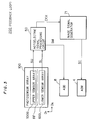
- Fig. 2 illustrates the overall structure of an image scan recorder 1 according to a preferred embodiment of the present invention.
- This image scan recorder 1 defines a process scanner of a flat bed type which comprises a polygon mirror 9 as a main deflector.
- Symbols X and Y shown in Fig. 2 denote a main scanning direction and a subscanning direction in an image scanning for recording an image, respectively.
- a laser beam LB emitted from a laser source 2 is divided into a main light beam LM and a reference light beam LR by a half mirror 3.
- An acousto-optical modulator (AOM) 4 which is controlled by an image signal SI, is arranged in an optical path of the main light beam LM, so that the main light beam LM is ON-OFF modulated by the AOM 4.
- the modulated main light beam LM is reflected by a mirror 5, and thereafter incident upon an acousto-optical deflector (AOD) 8 serving as a predeflector.
- AOD acousto-optical deflector
- the reference light beam LR is successively reflected by mirrors 6 and 7 to bypass the AOM 4, and enters the AOD 8 as a beam which is parallel to the main light beam LM.
- the AOD 8 which is supplied with a beam deviation signal SM as described later, deflects the light beams LM and LR in a direction F Y in response to the signal SM.
- the direction F Y is optically conjugate with the subscanning direction Y, and the light beams LM and LR are deflected substantially at the same angle.
- conjugate directions is used to indicate directions which are optically equivalent to each other on travelling paths of light beams.
- the light beams LM and LR deflected by the AOD 8 enter a polygon mirror 9, which rotates in a direction ⁇ at a constant velocity. Consequently, the light beams LM and LR are periodically deflected in a direction F X following rotation of the polygon mirror 9.
- the direction F X is optically conjugate with the main scanning direction X.
- the main light beam LM passes through a lens 10 and is thereafter reflected by a mirror 11 toward a photosensitive material 12.
- the main light beam LM scans the photosensitive material 12 along the main scanning direction X, to selectively expose its surface.
- a locus TL of this scanning defines a scanning line in image recording.
- the photosensitive material 12 is relatively moved by a moving mechanism (not shown) in the subscanning direction Y with respect to the main light beam LM, whereby a two-dimensional image which is responsive to the image signal SI is recorded on the photosensitive material 12 as a latent image.
- the reference light beam LR deflected by the polygon mirror 9 passes through the lens 10, and is thereafter incident upon a photosensor array 100.
- This photosensor array 100 is formed by linearly aligning and fixing a plurality of (e.g., six) photosensors 20a, 20b, ..., 20n on a long insulating substrate 40.
- the photosensor array 100 is so arranged that its elongated direction D X and cross direction D Y are optically conjugate with the main scanning direction X and the subscanning direction Y respectively.
- the photosensor array 100 is arranged in a position which is conjugate with respect to the locus TL of the main light beam LM on the photosensitive material 12.
- each of the photosensors 20a to 20n has an upper sensor and a lower sensor which are arrayed in parallel with each other.
- the respective upper sensors of the photosensors 20a to 20n are electrically interconnected to form an upper sensor array 100U.
- the respective lower sensors of the photosensors 20a to 20n are also electrically interconnected to form a lower sensor array 100L.
- the reference light beam LR which is received by the photosensor array 100 is photoelectrically converted by the upper and lower sensor arrays 100U and 100U, and the converted signals are outputted as a couple of photoelectric conversion signals SU and SL.
- Fig. 3 is a block diagram showing a feedback loop or closed loop controller 200 for performing modulation timing control in the AOM 4 and deflection control in the AOD 8 on the basis of the signals SU and SL.
- the signals SU and SL outputted from the upper and lower sensor arrays 100U and 100L are delivered to a photoelectric signal processing circuit 50.
- This processing circuit 50 generates a main scanning synchronizing clock (or grating clock) CKX and a beam deviation signal SM through signal processing as described later.
- the beam deviation signal SM is adapted to indicate how much an incident position of the reference light beam LR on the photosensor array 100 deviates from a reference line RF defined on the boundary between the upper and lower sensor arrays 100U and 100L.
- the beam deviation signal SM substantially expresses the amount of deflection of the main light beam LM on the photosensitive material 12 in the subscanning direction Y. Deflection of the light beams LM and LR in these directions Y and D Y is mainly caused by surface inclination of the polygon mirror 9.
- the beam deviation signal SM is supplied to the AOD 8 as a deflection control signal.
- the amounts of deflection of the light beams LM and LR in the AOD 8 are changed by the beam deviation signal SM, whereby the light beams LM and LR are controlled to regularly draw linear loci. Namely, deviations of projected positions of the light beams LM and LR in the subscanning direction Y and D Y caused by surface inclination of the polygon mirror 9 are compensated for by driving of the AOD 8 based on the beam deviation signal SM.
- the main scanning synchronizing clock CKX is supplied to an image signal generator 71.
- This image signal generator 71 may be adapted to perform prescribed processing on an image signal obtained by reading an original and outputting the same, or to successively read image signals previously stored in an image memory.
- An image signal SI which is generated in the form of a halftone dot signal in this image signal generator 71 is transmitted to the AOM 4 at timing defined by the main scanning synchronizing clock CKX every pixel.
- the AOM 4 ON/OFF-modulates the main light beam LM in response to the level of the image signal SI.
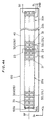
- Fig. 1 is a partially fragmented perspective view showing the structure of the photosensor 20a which is included in the photosensor array. Since the remaining photosensors 20b to 20n also have similar structures, only the photosensor 20a is now described.
- the photosensor 20a has a strip-shaped p-type semiconductor substrate 31 which extends in a direction D X .
- the major surface of the semiconductor substrate 31 is parallel to a plane which is defined by the directions D X and D Y .
- a pair of n-type semiconductor layers 32U and 32L are formed on this major surface.
- the n-type semiconductor layers 32U and 32L are in the form of strip-shaped wells extending in the direction D X , which are adjacent to each other at a small interval in the direction D Y .
- a pair of p-n junction regions JU and JL are defined by respective contact interfaces between the n-type semiconductor layers 32U and 32L and the p-type semiconductor substrate 31.
- the semiconductor layers 32U and 32L may be formed of a p-type semiconductor material in the case where the semiconductor substrate 31 is formed by an n-type substrate.
- the p-n junction regions JU and JL are adapted to photoelectrically convert light which enters from above in Fig. 1.
- the photosensor 20a comprises a pair of partial photosensors 21U and 21L which extend in the direction D X respectively.
- These partial sensors 21U and 21L, which are vertically arrayed in the positional relation shown in Fig. 2, are called upper and lower sensors respectively.
- a large number of unit light shielding layers 33 are arrayed above and over the n-type semiconductor layers 32U and 32L.
- the unit light shielding layers 33 are in the form of linear strips extending in the direction D Y , which are periodically arrayed along the direction D X to define a light shielding pattern (grating pattern) 34 as a whole.
- the light shielding pattern 34 is formed of aluminum, for example.
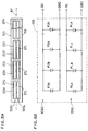
- Fig. 4A is a front elevational view showing the photosensor array 100.
- the plurality of photosensors 20a to 20n, each having the aforementioned structure, are arrayed on an insulating substrate 40 in ths direction D X .
- the n-type semiconductor layers 32U of the respective photosensors 20a to 20n are interconnected by electric wirings 32 which are typically shown in Fig. 4A, so that a first photoelectric conversion signal SU is taken out.
- the other n-type semiconductor layers 32L of the respective photosensors 20a to 20n are interconnected by other wirings 24, so that a second photoelectric conversion signal SL is taken out.
- the p-type semiconductor substrates 31 of the photosensors 20a to 20n are interconnected by wirings 25 or a printed metal layer provided on the surface of the insulated substrate 40, to be at a ground level GND.
- the photosensors 20a to 20n are so linearly aligned as to define the upper sensor array 100U as a set of the upper sensors 21U and the lower sensor array 100L as a set of the lower sensors 21L.
- the reference line RF which is an imaginary line, is defined along the boundary portion between the upper and lower sensor arrays 100U and 100L.
- Fig. 4B is an enlarged view showing a boundary portion between the photosensors 20a and 20b, which are adjacent to each other.
- Each of the unit light shielding layers 33 except for those provided at the ends of the photosensor 20a has a prescribed width W in the direction D X , and slit-type windows 35 provided between the adjacent unit light shielding layers 33 also have the same width W.
- This width W is at about the same value as the beam diameter of the reference light beam LR in the position of the photosensor array 100.
- Each of the two unit light shielding layers 33 provided at the ends of the photosensor 20a has a width W a smaller than the width W.
- An array gap G between the photosensors 20a and 20b is so determined that a distance between inner edges EA and EB of the unit light shielding layers 33 facing each other through the gap G coincides with the aforementioned width W.
- array of the windows 35 in the photosensor 20a is aligned in space with that of the windows 35 in the adjacent photosensor 20b.
- Such arrangement relation also applies to the remaining photosensors 20b to 20n.
- the windows 35 are arrayed in a same period (grating pitch) 2W throughout the overall photosensors 20a to 20n. Since the spatial adjustment of the photosensors 20a to 20n is attained only by adjusting the array gap of the photosensors 20a to 20n along the short sides of the photosensors, i.e., along the direction D Y , an operation for such adjustment is relatively simple as compared with the case where a plurality of photosensors are arranged in parallel in the direction D Y .
- the length of the photosensor array 100 along the direction D X is determined in proportion to the scanning range of the reference light beam LR along the direction D X at the position of the array 100. Since each of the photosensors 20a to 20n cannot have a length larger than the diameter of a semiconductor wafer employed for fabrication thereof, a sensing range corresponding to the aforementioned scanning range is ensured by forming the array of the plurality of photosensors 20a to 20n. Thus, the total number of the photosensors 20a to 20n which are included in the photosensor array 100 is determined by the ratio of the aforementioned scanning range to the length of each photosensor.
- Fig. 5 is a typical front elevational view of the photosensor array 100
- Fig. 5B is an equivalent circuit diagram of the photosensor array 100 which is drawn in correspondence to Fig. 5A.
- the light shielding pattern is omitted from Fig. 5A. Since the respective ones of the upper and lower sensors 21U and 21L have photoelectric conversion functions, the upper sensor array 100U is equivalent to parallel connection of photodiodes PU a to PU n , and the lower sensor array 100L is equivalent to parallel connection of photodiodes PL a to PL n .
- a composite output of the upper photodiodes PU a to PU n are taken out as the signal SU, while a composite output of the lower photodiodes PL a to PL n is taken out as the signal SL.
- the p-type semiconductor substrate 31 shown in Fig. 1 serves as an anode region which is common thereto, and hence there is no need to provide two ground wires as shown in Fig. 5B, but one ground line shown in Fig. 4A is sufficient.
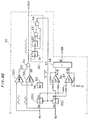
- Fig. 6A as combined with Fig. 6B is a circuit diagram showing the photoelectric signal processing circuit 50.
- the photoelectric conversion signals SU and SL from the upper and lower sensor arrays 100 U and 100L are subjected to current-to-voltage conversion by operational amplifiers 51U and 51L and inversion buffers IV U and IV L respectively.
- Voltage signals A O and B O thus obtained are inputted in comparators 52U and 52L respectively.
- a prescribed reference voltage V R from a reference voltage generator 53 is supplied as other inputs of the comparators 52U and 52L.
- Fig. 7 illustrates waveforms at respective parts of the photoelectric signal processing circuit 50 for respective scanning positions of a beam spot BS in the direction D X which is projected onto the photosensor array 100 by the reference light beam LR. As shown by one-dot chain lines, scales of the respective waveforms along the direction D X are enlarged as compared with those on the photosensor array 100. Fig. 7 illustrates the case where the central position of the beam spot BS upwardly deviates from the reference line RF.
- the signal A O obtained from the upper sensor array 100U when the beam spot BS passes through the windows 35 forms a wide peak.
- the signal B O obtained from the lower sensor array 100L forms a narrow peak.
- the comparators 52U and 52L compare these signals A O and B O with the common reference voltage V R , and output the results of comparison as binarized signals SA and SB respectively.
- the signal SA is a wide binary pulse
- the signal SB is a narrow binary pulse.
- a next-stage OR gate 54 calculates the logical sum of these signals SA and SB, and outputs the same as the main scanning synchronizing clock CKX.
- the clock CKX has the same waveform as the signal SA when the beam spot BS is an upwardly deviating state.
- the beam spot BS is in a downwardly deviating state, on the other hand, obtained are a set of waveforms in which the waveforms of the signals A O and B O shown in Fig. 7 are replaced with each other and those of the signals SA and SB are also replaced with each other.
- the clock CKX has the same waveform as the signal SB.
- the signals A O and B O have substantially identical waveforms, and a clock CKX is obtained by binarization of the common waveform.
- the one of the signals SA and SB having a larger pulse width is substantially utilized as the clock CKX. It is possible to set the pulse width CW of the clock CKX at about 50 % of the light shielding pattern cycle period 2W in terms of distance by adjusting the value of the reference voltage V R . Thus, the clock CKX becomes a pulse train having a duty ratio 1/2.
- the main scanning synchronizing clock CKX is supplied to the image signal generator 71 shown in Fig. 3, as well as to a timing generation circuit 60 shown in Fig. 6B.
- the clock CKX is subjected to a two-stage delay at delay circuits 61 and 62 of a two-stage structure provided in the timing generation circuit 60 (see Fig. 8A).
- a pulse train ST shown in the lower part of Fig. 8A is obtained by an exclusive OR gate 63 and a NAND gate 64 which are provided on a rear stage side thereof.
- This pulse train ST is a signal which forms a negative peak once every period when the reference light beam LR is projected into each window 35 of the photosensor array 100. It is possible to generate the negative peak in the pulse train ST at the center of the window 35, by adjusting the delay times in the delay circuits 61 and 62.
- This pulse train ST is supplied to sample-and-hold circuits 55U and 55L as timing control signals.
- the sample-and-hold circuits 55U and 55L samples the levels of the signals A O and B O respectively when the pulse train ST forms a negative peak, and hold the sampled levels until a next negative peak is formed.
- respective outputs A and B of the sample-and-hold circuits 55U and 55L become signals expressing previous peak values of the signals A O and B O as shown in Fig. 8B, so that values which are not zero can be maintained also when the beam spot BS is passing through the light shielding layer 33.
- surface inclination correction of the polygon mirror 9 based on the signals A and B can be continuously performed in time.
- the signals A and B are supplied to next stage operational amplifiers 56.
- the operational amplifier 56 serves as an analog subtracter, and the other operational amplifier 57 serves as an analog adder. Therefore, the operational amplifiers 56 and 57 output a difference signal (A - B) and a sum signal (A + B) respectively.
- This beam deviation signal SM is adapted to correct surface inclination of the polygon mirror 9 in real time, as already described above.
- the control signal for the AOD 8 is formed not by the difference signal (A - B) itself but by the normalized deviation M, whereby the deviation of the beam spot BS from the reference line RF is quantitatively and correctly expressed also when the light intensity of the reference light beam LR which is photoelectrically converted by the photosensor array 100 is not constant.
- the surface inclination of the polygon mirror is corrected in high accuracy.
- Figs. 9A to 9C are sectional views, taken along the lines IX - IX in Fig. 1, showing a method of manufacturing the photosensor 20a.
- the remaining photosensors 20b to 20n are also manufactured by a similar method.
- a p-type semiconductor wafer 91 (Fig. 9A) is prepared, and an n-type impurity is doped onto its upper major surface, to form an n-type semiconductor layer 92.
- An aluminum film 93 is formed on the n-type semiconductor layer 92 by vapor deposition, and thereafter a resist layer 94 having a periodic slit pattern is formed thereon.
- the aluminum film 93 is selectively etched through the resist layer 94, which serves as a mask (Fig. 9B).
- the resist layer 94 is removed, therefore, slit-type windows 35 and alternately arrayed unit light shielding layers 33 are obtained (Fig. 9C).
- the wafer is divided in the form of strips as shown in Fig. 1, to obtain the photosensor 20a.
- the semiconductor substrate 91 and the semiconductor layer 92 after such division are just the semiconductor substrate 31 and the semiconductor layer 32 shown in Fig. 1A, respectively.
- Accuracy for detection of deviation is increased as the distance between the pair of semiconductor layers 32U and 32L is reduced. If the distance is extremely reduced, however, an npn (or pnp) parasitic transistor is undesirably formed by the semiconductor layers 32U and 32L, serving as a collector and an emitter, and a portion of the semiconductor substrate 31, which is held between the semiconductor layers 32U and 32L, serving as a base.
- the aforementioned distance is preferably about 0.01 mm, for example.
- the grating pitch 2W is preferably about 0.8 mm, for example.
- the photosensor according to the present invention is also applicable to an image reading or recording apparatus employing a galvano mirror, a hologram disk or the like as a main deflector.
- an original surface is scanned with a main light beam so that its transmitted or reflected light is received by the photosensor, while timing for taking the photoreceptor signal in an image memory or the like is controlled by the main scanning synchronizing clock CKX.
- a method of correcting surface inclination etc. itself is similar to that in image recording.
- the reference light beam LR may be emitted from a light source which is different from that for the main light beam LM.
- two p-n junctions are formed on a common semiconductor layer in a parallel manner and the positional relation therebetween is fixed, whereby no assembled position control of high accuracy is required when the photosensor according to the present invention is is assembled into given apparatuses.
- the light shielding pattern is formed by array of simple strip-shaped light shielding layers which are directly formed on the sensor body, no grating glass member having a specific light shielding pattern is required. Consequently, it is possible to reduce the manufacturing cost.
- a photosensor array formed by arraying the aforementioned photosensor arrays along its longitudinal direction is employed, whereby the image scanner effectuates the aforementioned respective advantages.
Landscapes
- Engineering & Computer Science (AREA)
- Multimedia (AREA)
- Signal Processing (AREA)
- Facsimile Scanning Arrangements (AREA)
- Solid State Image Pick-Up Elements (AREA)
- Facsimile Heads (AREA)
Claims (10)
- Photosensor, der zur Feststellung einer Abtastposition eines Lichtstrahls verwendbar ist, mit(a) einer ersten Halbleiterschicht (31) eines ersten Leitfähigkeitstyps mit einer Hauptfläche, die durch erste und zweite Richtungen (Dx, Dy) definiert ist und sich längs der ersten Richtung (Dx) in Form eines Streifen erstreckt, wobei die erste Richtung (Dx) einer Abtastrichtung des Lichtstrahls entspricht und die zweite Richtung (Dy) senkrecht zur ersten Richtung ist,(b) einem Paar von zweiten Halbleiterschichten (32U, 32L) eines zweiten Leitfähigkeitstyps, die in der Hauptfläche längs der ersten Richtung (Dx) in Form von Streifen ausgebildet sind und in der zweiten Richtung (Dy) benachbart zueinander liegen, gekennzeichnet durch(c) ein an der Hauptfläche anhaftendes Abschirmmuster, welches Einheits-Lichtabschirmschichten (33) aufweist, von denen jede streifenförmig ist und sich längs der zweiten Richtung (Dy) erstreckt, und welche periodisch längs der ersten Richtung (Dx) mit Zwischenräumen (35) dazwischen angeordnet sind und ausgewählt das Paar von zweiten Halbleiterschichten (32U, 32L) abdecken,wobei erste und zweite photoelektrische Umwandlungssignale, die die Abtastposition des Lichtstrahls angeben, aus ersten und zweiten pn-Übergängen, die zwischen der ersten Halbleiterschicht und betreffenden des Paares von zweiten Halbleiterschichten definiert sind, gewonnen werden, wenn die Hauptfläche mit dem Lichtstrahl abgetastet wird.
- Photosensor nach Anspruch 1, wobeijeder der Zwischenräume (35) die gleiche Breite wie jede der Einheitsabschirmschichten (33) in der ersten Richtung (Dx) hat.
- Photosensor nach Anspruch 2, wobeidie Breite im wesentlichen gleich einem Durchmesser des Lichtstrahls auf der Hauptfläche ist.
- Photosensor nach Anspruch 2 oder 3, wobeidas Lichtabschirmmuster ferner zusätzliche Abschirmschichten aufweist, die an entgegengesetzten Endflächen der Hauptfläche vorgesehen sind und sich längs der zweiten Richtung mit solchen Zwischenräumen zwischen den Einheits-Abschirmschichten (33) und den zusätzlichen Lichtabschirmschichten erstrecken, so daß ausgewählt betreffende Enden des Paares von zweiten Halbleiterschichten abgedeckt werden, wobei die zusätzlichen Lichtabschirmschichten eine Breite haben, die kleiner als die Breite einer jeden Einheits-Lichtabschirmschicht ist.
- Photosensor nach irgendeinem der Ansprüche 1 bis 4, wobeidas Lichtabschirmmuster aus Metall besteht.
- Photosensorfeld, welches zur Feststellung einer Abtastposition eines Lichtstrahls verwendbar ist, mit einer Anzahl von Photosensoren nach Anspruch 4, ausgerichtet auf einer Platte (40) in der ersten Richtung (Dx), wobeidie Photosensoren in der ersten Richtung mit Ausrichtungszwischenräumen (G) zwischen ihnen ausgerichtet sind, wobei jeder der Ausrichtungszwischenräume von solcher Art ist, daß die folgende Gleichung gilt:
 Wa die Breite einer jeden zusätzlichen Lichtabschirmschicht ist,G ein Wert ist, der jeden der Ausrichtungszwischenräume darstellt, undW die Breite eines jeden Einheits-Lichtabschirmmusters ist.
 - Bildabtaster zum periodischen Abtasten einer Objektoberfläche (12) mit einem Hauptlichtstahl (LM) in einer vorgegebenen Hauptabtastrichtung (X) und Relativbewegen der abgetasteten Oberfläche (12) und des Hauptlichtstrahls (LM) längs einer Nebenabtastrichtung (X), womit eine Bildaufzeichnung auf der Objektoberfläche oder ein Bildlesen von der Objektoberfläche durchgeführt wird, mit einem Photosensorfeld gemäß Anspruch 6, wobei die Photosensoren (20a, ... 20n) desselben in einer ersten Richtung (Dx) konjugiert zur Hauptablenkrichtung (X) linear angeordnet sind und an einer Stelle liegen, die den Referenzlichtstrahl (LR) empfangen kann, wobei der Bildabtaster(a) Lichtstrahlabgabemittel (2, 3, 6) zum Abgeben des Hauptlichtstrahls (LM) unter gleichzeitiger Abgabe eines Referenzlichtstrahls (LR), der zu dem Hauptlichtstrahl parallel ist,(b) einen Vorablenker (8), der im optischen Weg von Hauptund Referenzlichtstrahl liegt, zum Ablenken von Haupt- und Referenzlichtstrahl in eine Vorablenkrichtung (Fy), die zu der Nebenabtastrichtung (Y) konjugiert ist, ansprechend auf ein Steuersignal,(c) einen Hauptablenker (9) für den Empfang von Haupt- und Referenzlichtstrahls nach Ablenkung durch den Vorablenker (8) und zum periodischen Ablenken von Haupt- und Referenzlichtstrahl in eine Hauptablenkrichtung (Fx), welche zur Hauptabtastrichtung (X) konjugiert ist,(d) Mittel (11) zum relativen Ändern betreffender Lauf richtungen von Haupt- und Referenzlichtstrahl nach Ablenkung durch den Hauptablenker, wodurch nur der Hauptlichtstrahl auf die abgetastete Oberfläche geleitet wird,(e) Mittel zum Aufsummieren betreffender in den Photosensoren gewonnener erster photoelektrischer Umwandlungssignale zur Erzeugung eines ersten zusammengesetzten Signals (SU),(f) Mittel zum Aufsummieren betreffender in den Photosensoren gewonnener zweiter photoelektrischer Umwandlungssignale zur Erzeugung eines zweiten zusammengesetzten Signals (SL), und(g) Rückkopplungsmittel (50) für den Empfang von erstem und zweitem zusammengesetzten Signal zur Erzeugungeines Rückkopplungssignals (SM) ansprechend auf die Differenz zwischen erstem und zweitem zusammengesetzten Signal, wobei das Rückkopplungssignal an den Vorablenker (8) als das Steuersignal geliefert wird, undeines Zeitsignals (CKX) zur Bestimmung einer Zeit für das Bildaufzeichnen oder Bildlesen mit dem Hauptlichtstrahl auf der Objektoberfläche aufweist.
- Bildabtaster nach Anspruch 7, wobeidie Rückkopplungsmittel (50)(h-1) Mittel (52U, 52L) zur Binarisierung von erstem und zweitem zusammengestzten Signal zur Gewinnung eines ersten und zweiten Binärsignals (SA, SB), und(h-2) Mittel (54) zur Gewinnung einer logischen Summe von erstem und zweitem Binärsignal zur Erzeugung des Zeitsignals aufweisen.
- Bildabtaster nach Anspruch 8, wobeidie Rückkopplungsmittel (50) ferner(h-3) Mittel (55U, 55L) zum Abtasten und Halten betreffender Spitzenwerte des ersten und zweiten zusammengesetzten Signals sychron mit dem Zeitsignal zur Gewinnung von eines ersten und zweiten elektrischen Signals (A, B), aus welchen das Rückkopplungssignal gewonnen wird, aufweisen.
- Bildabtaster nach Anspruch 9, wobeidie Rückkopplungsmittel (50) ferner(h-4) Mittel (56) zum Berechnen einer Differenz zwischen dem ersten und zweiten elektrischen Signal zur Gewinnung eines Differenzsignals (A-B),(h-5) Mittel (57) zum Berechnen einer Summe aus erstem und zweitem elektrischen Signal zur Gewinnung eines Summensignals (A+B), und(h-6) Mittel (58) zum Dividieren des Differenzsignals durch das Summensignal zur Erzeugung des Rückkopplungssignals (SM) aufweisen.
Applications Claiming Priority (2)
| Application Number | Priority Date | Filing Date | Title |
|---|---|---|---|
| JP2067850A JPH03266463A (ja) | 1990-03-15 | 1990-03-15 | フォトセンサおよびそれを用いた画像走査装置 |
| JP67850/90 | 1990-03-15 |
Publications (3)
| Publication Number | Publication Date |
|---|---|
| EP0446812A2 EP0446812A2 (de) | 1991-09-18 |
| EP0446812A3 EP0446812A3 (en) | 1992-07-15 |
| EP0446812B1 true EP0446812B1 (de) | 1996-03-06 |
Family
ID=13356849
Family Applications (1)
| Application Number | Title | Priority Date | Filing Date |
|---|---|---|---|
| EP91103607A Expired - Lifetime EP0446812B1 (de) | 1990-03-15 | 1991-03-08 | Fotodetektor und Bildabtaster dafür |
Country Status (4)
| Country | Link |
|---|---|
| US (1) | US5153422A (de) |
| EP (1) | EP0446812B1 (de) |
| JP (1) | JPH03266463A (de) |
| DE (1) | DE69117547T2 (de) |
Families Citing this family (5)
| Publication number | Priority date | Publication date | Assignee | Title |
|---|---|---|---|---|
| US5818507A (en) * | 1994-10-28 | 1998-10-06 | Xerox Corporation | Method and apparatus for controlling the modulation of light beams in a rotating polygon type image forming apparatus |
| JP3239072B2 (ja) * | 1996-09-03 | 2001-12-17 | 株式会社東芝 | ビーム光走査装置および画像形成装置 |
| GB2370172B (en) * | 2000-12-13 | 2002-12-04 | Infrared Integrated Syst Ltd | Dynamic offset correction in detector arrays |
| DE10157244B4 (de) * | 2001-11-22 | 2006-05-04 | Leica Microsystems Semiconductor Gmbh | Verfahren und Vorrichtung zur Defektanalyse von Wafern |
| JP2007081185A (ja) * | 2005-09-15 | 2007-03-29 | Fujifilm Corp | 光検出素子 |
Family Cites Families (8)
| Publication number | Priority date | Publication date | Assignee | Title |
|---|---|---|---|---|
| US3609375A (en) * | 1968-07-19 | 1971-09-28 | Trw Inc | Solid state linear photosensor |
| US4214157A (en) * | 1978-07-07 | 1980-07-22 | Pitney Bowes, Inc. | Apparatus and method for correcting imperfection in a polygon used for laser scanning |
| JPS57145368A (en) * | 1981-03-04 | 1982-09-08 | Hitachi Ltd | Semiconductor intergrated circuit |
| JPS58207767A (ja) * | 1982-05-28 | 1983-12-03 | Matsushita Electric Ind Co Ltd | 一次元固体撮像装置 |
| US4661699A (en) * | 1983-03-28 | 1987-04-28 | T. R. Whitney Corporation | Scanning beam control system and method with bi-directional reference scale |
| IL80242A (en) * | 1986-10-07 | 1994-01-25 | Scitex Corp Ltd | Laser scanner |
| US4837588A (en) * | 1987-05-08 | 1989-06-06 | Ricoh Company, Ltd. | Synchronizing signal generating system for laser scanner |
| US4882490A (en) * | 1987-09-22 | 1989-11-21 | Fuji Photo Film Co., Ltd. | Light beam scanning apparatus having two detectors whose signal ratio indicates main scanning position |
-
1990
- 1990-03-15 JP JP2067850A patent/JPH03266463A/ja active Pending
-
1991
- 1991-03-05 US US07/665,515 patent/US5153422A/en not_active Expired - Fee Related
- 1991-03-08 DE DE69117547T patent/DE69117547T2/de not_active Expired - Fee Related
- 1991-03-08 EP EP91103607A patent/EP0446812B1/de not_active Expired - Lifetime
Also Published As
| Publication number | Publication date |
|---|---|
| DE69117547T2 (de) | 1996-10-24 |
| DE69117547D1 (de) | 1996-04-11 |
| EP0446812A3 (en) | 1992-07-15 |
| EP0446812A2 (de) | 1991-09-18 |
| JPH03266463A (ja) | 1991-11-27 |
| US5153422A (en) | 1992-10-06 |
Similar Documents
| Publication | Publication Date | Title |
|---|---|---|
| US5359434A (en) | Scanning optical apparatus | |
| US4829175A (en) | Light beam scanning apparatus, method of correcting unevenness in scanning lines in light beam scanning apparatus, method of detecting deflection of rotational axis of light beam deflector and rotational axis deflection detecting device | |
| US4694164A (en) | Light beam scanning apparatus | |
| EP0596641B1 (de) | Verfahren und Vorrichtung zur Bildausrichtung | |
| US5640188A (en) | Multiple diode laser employing mating substrates | |
| JP2657505B2 (ja) | マーク位置検出装置およびマーク配置方法 | |
| US5012089A (en) | Scanning beam control system and optical scale structure useful thereto | |
| JPH0150886B2 (de) | ||
| EP0446812B1 (de) | Fotodetektor und Bildabtaster dafür | |
| US4845530A (en) | Reduced projection type step- and repeat-exposure apparatus | |
| EP0549204B1 (de) | Kontrolle der Strahlposition für ein Abtastgerät | |
| US4578577A (en) | Light beam scanning device | |
| JPH1010446A (ja) | マルチ光ビーム走査の同期検出方法及びマルチ光ビーム走査装置 | |
| JP3065865B2 (ja) | 光ビーム走査装置 | |
| JPH10177145A (ja) | マルチビーム光走査装置 | |
| JPH06100730B2 (ja) | 光ビーム走査装置 | |
| JPS63257714A (ja) | 光ビ−ム走査装置 | |
| JP2002250882A (ja) | マルチビーム走査装置 | |
| JPH0473567B2 (de) | ||
| JPH03295354A (ja) | 画像読取装置 | |
| JPH0367213A (ja) | 光ビームの照射位置検出装置 | |
| JPH03202726A (ja) | 光ビーム検出センサ | |
| JP2788846B2 (ja) | 円筒内面走査装置 | |
| JP3040881B2 (ja) | 光ビーム径測定装置 | |
| JPS6125118A (ja) | レ−ザプリンタ |
Legal Events
| Date | Code | Title | Description |
|---|---|---|---|
| PUAI | Public reference made under article 153(3) epc to a published international application that has entered the european phase |
Free format text: ORIGINAL CODE: 0009012 |
|
| AK | Designated contracting states |
Kind code of ref document: A2 Designated state(s): DE FR GB |
|
| PUAL | Search report despatched |
Free format text: ORIGINAL CODE: 0009013 |
|
| AK | Designated contracting states |
Kind code of ref document: A3 Designated state(s): DE FR GB |
|
| 17P | Request for examination filed |
Effective date: 19921015 |
|
| 17Q | First examination report despatched |
Effective date: 19940905 |
|
| GRAA | (expected) grant |
Free format text: ORIGINAL CODE: 0009210 |
|
| AK | Designated contracting states |
Kind code of ref document: B1 Designated state(s): DE FR GB |
|
| PG25 | Lapsed in a contracting state [announced via postgrant information from national office to epo] |
Ref country code: FR Effective date: 19960306 |
|
| REF | Corresponds to: |
Ref document number: 69117547 Country of ref document: DE Date of ref document: 19960411 |
|
| EN | Fr: translation not filed | ||
| PLBE | No opposition filed within time limit |
Free format text: ORIGINAL CODE: 0009261 |
|
| STAA | Information on the status of an ep patent application or granted ep patent |
Free format text: STATUS: NO OPPOSITION FILED WITHIN TIME LIMIT |
|
| 26N | No opposition filed | ||
| PGFP | Annual fee paid to national office [announced via postgrant information from national office to epo] |
Ref country code: DE Payment date: 20000306 Year of fee payment: 10 |
|
| PGFP | Annual fee paid to national office [announced via postgrant information from national office to epo] |
Ref country code: GB Payment date: 20000308 Year of fee payment: 10 |
|
| PG25 | Lapsed in a contracting state [announced via postgrant information from national office to epo] |
Ref country code: GB Free format text: LAPSE BECAUSE OF NON-PAYMENT OF DUE FEES Effective date: 20010308 |
|
| GBPC | Gb: european patent ceased through non-payment of renewal fee |
Effective date: 20010308 |
|
| PG25 | Lapsed in a contracting state [announced via postgrant information from national office to epo] |
Ref country code: DE Free format text: LAPSE BECAUSE OF NON-PAYMENT OF DUE FEES Effective date: 20020101 |