EP0446657B1 - Verfahren zur Vorbereitung einer Blende zur Verminderung von Teilchen in einer Kammer zur physikalischen Aufdampfung - Google Patents
Verfahren zur Vorbereitung einer Blende zur Verminderung von Teilchen in einer Kammer zur physikalischen Aufdampfung Download PDFInfo
- Publication number
- EP0446657B1 EP0446657B1 EP91102324A EP91102324A EP0446657B1 EP 0446657 B1 EP0446657 B1 EP 0446657B1 EP 91102324 A EP91102324 A EP 91102324A EP 91102324 A EP91102324 A EP 91102324A EP 0446657 B1 EP0446657 B1 EP 0446657B1
- Authority
- EP
- European Patent Office
- Prior art keywords
- shield
- plate
- chamber
- plasma
- vapor deposition
- Prior art date
- Legal status (The legal status is an assumption and is not a legal conclusion. Google has not performed a legal analysis and makes no representation as to the accuracy of the status listed.)
- Expired - Lifetime
Links
- 238000005240 physical vapour deposition Methods 0.000 title claims description 38
- 238000000034 method Methods 0.000 title claims description 26
- 239000002245 particle Substances 0.000 title description 3
- 238000004140 cleaning Methods 0.000 claims description 21
- XKRFYHLGVUSROY-UHFFFAOYSA-N Argon Chemical compound [Ar] XKRFYHLGVUSROY-UHFFFAOYSA-N 0.000 claims description 13
- 229910052786 argon Inorganic materials 0.000 claims description 7
- 238000004544 sputter deposition Methods 0.000 claims description 7
- 238000003795 desorption Methods 0.000 claims description 4
- 238000011144 upstream manufacturing Methods 0.000 claims description 3
- 239000011261 inert gas Substances 0.000 claims description 2
- 230000004913 activation Effects 0.000 claims 1
- 238000005137 deposition process Methods 0.000 claims 1
- 238000005019 vapor deposition process Methods 0.000 claims 1
- 239000000463 material Substances 0.000 description 19
- 235000012431 wafers Nutrition 0.000 description 16
- 230000008569 process Effects 0.000 description 11
- 239000011324 bead Substances 0.000 description 7
- 238000005422 blasting Methods 0.000 description 5
- 239000007789 gas Substances 0.000 description 5
- 150000002500 ions Chemical class 0.000 description 5
- MAKDTFFYCIMFQP-UHFFFAOYSA-N titanium tungsten Chemical compound [Ti].[W] MAKDTFFYCIMFQP-UHFFFAOYSA-N 0.000 description 4
- 238000011109 contamination Methods 0.000 description 3
- 238000000151 deposition Methods 0.000 description 3
- 230000008021 deposition Effects 0.000 description 3
- 238000011065 in-situ storage Methods 0.000 description 3
- 230000001788 irregular Effects 0.000 description 3
- 238000002360 preparation method Methods 0.000 description 3
- 229910001080 W alloy Inorganic materials 0.000 description 2
- 229910052782 aluminium Inorganic materials 0.000 description 2
- XAGFODPZIPBFFR-UHFFFAOYSA-N aluminium Chemical compound [Al] XAGFODPZIPBFFR-UHFFFAOYSA-N 0.000 description 2
- 230000004888 barrier function Effects 0.000 description 2
- 238000009792 diffusion process Methods 0.000 description 2
- 238000005530 etching Methods 0.000 description 2
- 229910052751 metal Inorganic materials 0.000 description 2
- 239000002184 metal Substances 0.000 description 2
- 238000005289 physical deposition Methods 0.000 description 2
- 239000010935 stainless steel Substances 0.000 description 2
- 229910001220 stainless steel Inorganic materials 0.000 description 2
- 230000003746 surface roughness Effects 0.000 description 2
- 229910000838 Al alloy Inorganic materials 0.000 description 1
- -1 Argon ions Chemical class 0.000 description 1
- UFHFLCQGNIYNRP-UHFFFAOYSA-N Hydrogen Chemical compound [H][H] UFHFLCQGNIYNRP-UHFFFAOYSA-N 0.000 description 1
- ZOKXTWBITQBERF-UHFFFAOYSA-N Molybdenum Chemical compound [Mo] ZOKXTWBITQBERF-UHFFFAOYSA-N 0.000 description 1
- RTAQQCXQSZGOHL-UHFFFAOYSA-N Titanium Chemical compound [Ti] RTAQQCXQSZGOHL-UHFFFAOYSA-N 0.000 description 1
- NRTOMJZYCJJWKI-UHFFFAOYSA-N Titanium nitride Chemical group [Ti]#N NRTOMJZYCJJWKI-UHFFFAOYSA-N 0.000 description 1
- 230000009471 action Effects 0.000 description 1
- QVGXLLKOCUKJST-UHFFFAOYSA-N atomic oxygen Chemical compound [O] QVGXLLKOCUKJST-UHFFFAOYSA-N 0.000 description 1
- 230000008901 benefit Effects 0.000 description 1
- 230000015572 biosynthetic process Effects 0.000 description 1
- 230000008859 change Effects 0.000 description 1
- 230000006835 compression Effects 0.000 description 1
- 238000007906 compression Methods 0.000 description 1
- 230000007547 defect Effects 0.000 description 1
- 238000010586 diagram Methods 0.000 description 1
- 230000000694 effects Effects 0.000 description 1
- 239000001307 helium Substances 0.000 description 1
- 229910052734 helium Inorganic materials 0.000 description 1
- SWQJXJOGLNCZEY-UHFFFAOYSA-N helium atom Chemical compound [He] SWQJXJOGLNCZEY-UHFFFAOYSA-N 0.000 description 1
- 239000001257 hydrogen Substances 0.000 description 1
- 229910052739 hydrogen Inorganic materials 0.000 description 1
- 239000012212 insulator Substances 0.000 description 1
- 229910052743 krypton Inorganic materials 0.000 description 1
- DNNSSWSSYDEUBZ-UHFFFAOYSA-N krypton atom Chemical compound [Kr] DNNSSWSSYDEUBZ-UHFFFAOYSA-N 0.000 description 1
- 239000007788 liquid Substances 0.000 description 1
- 238000004519 manufacturing process Methods 0.000 description 1
- 239000007769 metal material Substances 0.000 description 1
- 229910052750 molybdenum Inorganic materials 0.000 description 1
- 239000011733 molybdenum Substances 0.000 description 1
- 229910052754 neon Inorganic materials 0.000 description 1
- GKAOGPIIYCISHV-UHFFFAOYSA-N neon atom Chemical compound [Ne] GKAOGPIIYCISHV-UHFFFAOYSA-N 0.000 description 1
- 230000006911 nucleation Effects 0.000 description 1
- 238000010899 nucleation Methods 0.000 description 1
- TWNQGVIAIRXVLR-UHFFFAOYSA-N oxo(oxoalumanyloxy)alumane Chemical compound O=[Al]O[Al]=O TWNQGVIAIRXVLR-UHFFFAOYSA-N 0.000 description 1
- 239000001301 oxygen Substances 0.000 description 1
- 229910052760 oxygen Inorganic materials 0.000 description 1
- 238000009832 plasma treatment Methods 0.000 description 1
- 239000000843 powder Substances 0.000 description 1
- 230000001902 propagating effect Effects 0.000 description 1
- 238000005086 pumping Methods 0.000 description 1
- 230000009467 reduction Effects 0.000 description 1
- 238000005488 sandblasting Methods 0.000 description 1
- 239000004065 semiconductor Substances 0.000 description 1
- 239000007787 solid Substances 0.000 description 1
- 239000013077 target material Substances 0.000 description 1
- 239000010936 titanium Substances 0.000 description 1
- 229910052719 titanium Inorganic materials 0.000 description 1
- WFKWXMTUELFFGS-UHFFFAOYSA-N tungsten Chemical compound [W] WFKWXMTUELFFGS-UHFFFAOYSA-N 0.000 description 1
- 229910052721 tungsten Inorganic materials 0.000 description 1
- 239000010937 tungsten Substances 0.000 description 1
- 238000013022 venting Methods 0.000 description 1
- XLYOFNOQVPJJNP-UHFFFAOYSA-N water Substances O XLYOFNOQVPJJNP-UHFFFAOYSA-N 0.000 description 1
Images


Classifications
-
- C—CHEMISTRY; METALLURGY
- C23—COATING METALLIC MATERIAL; COATING MATERIAL WITH METALLIC MATERIAL; CHEMICAL SURFACE TREATMENT; DIFFUSION TREATMENT OF METALLIC MATERIAL; COATING BY VACUUM EVAPORATION, BY SPUTTERING, BY ION IMPLANTATION OR BY CHEMICAL VAPOUR DEPOSITION, IN GENERAL; INHIBITING CORROSION OF METALLIC MATERIAL OR INCRUSTATION IN GENERAL
- C23C—COATING METALLIC MATERIAL; COATING MATERIAL WITH METALLIC MATERIAL; SURFACE TREATMENT OF METALLIC MATERIAL BY DIFFUSION INTO THE SURFACE, BY CHEMICAL CONVERSION OR SUBSTITUTION; COATING BY VACUUM EVAPORATION, BY SPUTTERING, BY ION IMPLANTATION OR BY CHEMICAL VAPOUR DEPOSITION, IN GENERAL
- C23C14/00—Coating by vacuum evaporation, by sputtering or by ion implantation of the coating forming material
- C23C14/22—Coating by vacuum evaporation, by sputtering or by ion implantation of the coating forming material characterised by the process of coating
- C23C14/56—Apparatus specially adapted for continuous coating; Arrangements for maintaining the vacuum, e.g. vacuum locks
- C23C14/564—Means for minimising impurities in the coating chamber such as dust, moisture, residual gases
-
- C—CHEMISTRY; METALLURGY
- C23—COATING METALLIC MATERIAL; COATING MATERIAL WITH METALLIC MATERIAL; CHEMICAL SURFACE TREATMENT; DIFFUSION TREATMENT OF METALLIC MATERIAL; COATING BY VACUUM EVAPORATION, BY SPUTTERING, BY ION IMPLANTATION OR BY CHEMICAL VAPOUR DEPOSITION, IN GENERAL; INHIBITING CORROSION OF METALLIC MATERIAL OR INCRUSTATION IN GENERAL
- C23C—COATING METALLIC MATERIAL; COATING MATERIAL WITH METALLIC MATERIAL; SURFACE TREATMENT OF METALLIC MATERIAL BY DIFFUSION INTO THE SURFACE, BY CHEMICAL CONVERSION OR SUBSTITUTION; COATING BY VACUUM EVAPORATION, BY SPUTTERING, BY ION IMPLANTATION OR BY CHEMICAL VAPOUR DEPOSITION, IN GENERAL
- C23C14/00—Coating by vacuum evaporation, by sputtering or by ion implantation of the coating forming material
- C23C14/02—Pretreatment of the material to be coated
- C23C14/021—Cleaning or etching treatments
Definitions
- the present invention concerns the preparation of shields in a physical vapor deposition chamber in order to increase shield adhesion and thereby achieve particle reduction.
- PVD physical vapor deposition
- a target material for example Titanium Tungsten
- gaseous ions for example Argon ions.
- Material from the target is dislodged and sputters onto a work piece.
- the work piece is generally a semiconductor wafer, but may be, for example, a magnetic disk or a flat panel display.
- a PVD chamber generally includes shields in the area immediately around a wafer.
- the shields prevent excess material sputtering from the target from contaminating the remainder of the PVD chamber.
- the above mentioned problems have been overcome with the methods as claimed in claims 1 and 5.
- the invention further relates to a physical vapor deposition chamber as claimed in claims 10 and 12.
- a method for preparing a shield for use in a physical vapor deposition process.
- the shield is sputter-etch cleaned to increase adhesion of deposits in the physical vapor deposition process.
- the sputter-etch cleaning serves to loosen contamination, such as oxides of the shield material, which may form a diffusion barrier and prevent the deposits from bonding to the shield.
- the sputter-etch cleaning creates a high degree of surface roughness. This roughness allows for an increase in the ability of a sputtered film to mechanically adhere to the shield.
- the shield may first be bead blasted.
- the bead blasting makes the surface of the shield irregular. This enhances interface crack propagation of deposited material on a submicroscopic scale and hinders the flaking of deposited material. This is because the surface irregularities force a fracture propagating along a plane of weakness to often change direction or pass through a stronger region.
- Figure 1 is a simplified block diagram showing a physical vapor deposition chamber used for a sputter deposition process.
- Figure 2 shows a perspective view of a disassembled physical vapor deposition chamber in accordance with the preferred embodiment of the present invention.
- Figure 3 shows a physical deposition chamber arranged to sputter-etch clean a shield in accordance with a preferred embodiment of the present invention.
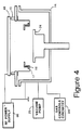
- Figure 4 shows a physical deposition chamber in which an RF power signal is placed on a lid for in situ reactive or non-reactive plasma treatment of a shield and a clamping ring in accordance with an alternate embodiment of the present invention.
- a physical vapor deposition (PVD) chamber 14 includes a movable wafer table 24.
- a specimen i.e., a wafer 36
- Wafer table 24 is raised through a clamping ring 16 and a shield 17 to a processing location.
- An RF wafer bias circuit 12 provides an RF bias voltage to the wafer.
- a DC wafer bias circuit 13 provides a DC bias to the wafer through a line 18.
- Gas control circuitry 26 controls gas flow in and out of chamber 14.
- a vacuum pump 25 is used to create a vacuum in PVD chamber 14 during processing of wafers.
- a source 20 has a sputter target 22 composed of, for example, Titanium-Tungsten alloy.
- Source 20 is electrically isolated from shield 17 and the rest of PVD chamber 14 by an insulator ring 10.
- a DC power supply 21 establishes a voltage potential between shield 17 and source 20.
- the negative terminal of DC power supply 21 is connected to target 22.
- the positive terminal is grounded to PVD chamber 14. This operating mode is used because gaseous ions from plasma will be accelerated toward whatever surface is connected to the negative terminal of power supply 21.
- ions in deposition plasma strike target 22 and cause sputtering of Titanium-Tungsten alloy onto wafer 36 on wafer table 24.
- FIG. 2 shows PVD chamber 14, shield 17, and clamping ring 16.
- Chamber 14 is shown to include ports 27, 28, 29, 30, 31, 32, and 33.
- Port 30 may be used, for example, by vacuum pump 25 or by a roughing pump for initial pumping to create a vacuum.
- Port 33 may be, for example, used by a residual gas analyzer.
- Port 32 may be, for example, used to allow a power line into PVD chamber 14, for example, to power a lamp used in PVD.
- Port 27 may be, for example, used for venting.
- Port 29 may be, for example, used as a window.
- Port 28 may be, for example, used for supplying Argon gas and reactive gas into chamber 14. Wafers are placed in PVD chamber 14 through an opening 31 by automated machinery (not shown).
- Titanium Tungsten (TiW) material is deposited on shield 17 and clamping ring 16. This material builds up and eventually begins to flake. The flaking results in unwanted particles contaminating PVD chamber 14.
- the present invention pertains to preparing the surface of shield 17 to increase adhesion of excess material to the shield.
- the adhesion strength of TiW depends on both the bonding strength between the TiW and the material of which shield 17 is made, and it depends on the microstructure of the interface region between the TiW and shield 17.
- shield 17 may be sputter-etch cleaned before usage.
- the sputter-etch cleaning serves to loosen contamination which may form a diffusion barrier and prevent the TiW from bonding to shield 17.
- the sputter-etch cleaning creates a high density of micro surface roughness. These defects allow for an increase in nucleation sites which minimize the formation of interface voids.
- sputter-etch cleaning of the shields is done in a chamber from which source 20 is removed.
- source 20 is replaced with a flat cover plate 46 fabricated of aluminum alloy, stainless steel, or some other vacuum compatible metallic material.
- cover plate 46 In the center of cover plate 46 is mounted an arrangement of permanent magnets 34 which does not exceed half of the chamber lid size in diameter.
- cover plate 46 is biased positive to a value between +300 volts and +1000 volts. Cover plate 46 thus becomes the anode of a glow discharge in the vacuum chamber. Power in the range of 50 Watts to 500 Watts is applied to cover plate 46.
- the negative terminal of power supply 21 is grounded to PVD chamber 14, shield 17 and clamping ring 16.
- the preferred operating ambient is 0.5 - 2 Pa (three to twelve Millitorr) of Argon.
- Magnet assembly 34 is used to maintain plasma operation at the low operating pressures where the process is most efficient at etching the grounded shield 17 and clamping ring 16.
- Alternate means of striking the shield etch plasma include momentary application of high pressure in the range of 7-70 Pa (50 Millitorr to 500 Millitorr) and include the momentary application of a high voltage AC or DC.
- Two types of power supplies may be used to maintain the plasma. The first is a constant-power power supply with a rating of 1000 Volts and 1 kilowatt. The second is a 1000 Volt constant-voltage power supply used in conjunction with a high power ballast resistor 35.
- shield 17 may typically be cleaned to a satisfactory degree after several minutes of the etch process.
- shield 17 may be bead blasted.
- the bead blasting is done by bombarding shield 17 and clamping ring 16 with aluminum oxide abrasive powder.
- the bead blasting may be done in a commercially available sand blasting chamber.
- the bead blasting makes the surface of shield 17 irregular.
- the irregular surface on a microscopic scale, will enhance interface crack propagation of TiW material which is later deposited on shield 17.
- the surface irregularities will result in the breaking up of the deposited films into sections are small with respect to flake sizes. This significantly hinders flaking.
- the rough surface provides a greater surface area.
- the rough surface distributes stress, that is, when one side of a ridge is in tensile stress, the other side of the ridge is in compression stress.
- shield 17 and clamping ring 16 are important to maximize adhesion. Shields made of Titanium, stainless steel covered with a film of Aluminum, Aluminum or Molybdenum have proved to provide satisfactory adhesion.
- shield 17 and clamping ring 16 design of shield 17 and clamping ring 16 to maximize the surface on which excess TiW material is deposited reduces the thickness of the deposits.
- the discussion of the preferred embodiment has focussed on increasing adhesion of TiW material to shield 17, the invention is applicable to increasing adhesion of other materials used in physical vapor deposition chamber.
- the invention may be used to increase adhesion from excess material from depositions of pure Tungsten or a reactive deposition of Titanium nitride.
- shield 17 and clamping ring 16 may be cleaned by gentle bombardment of a plasma (i.e., plasma cleaning) below the threshold and under process conditions where no shield etch material is physically removed.
- a plasma i.e., plasma cleaning
- the surface of shield 17 and clamping ring 16 may be reacted in an oxygen plasma to intentionally produce an oxide scale to which certain sputtered materials might readily adhere.
- oxide scale on shield 17 and clamping ring 16 could be removed without the evolution of sputtered metal atoms through the action of a hydrogen plasma.
- Such reactive processes could be performed in situ in PVD chamber 14.
- PVD chamber 14 is shown modified to facilitate plasma cleaning.
- An RF power signal at an ISM frequency (e.g., 13.56 Megahertz) is applied to cover plate 46 of PVD chamber 14 by RF power supply 66.
- ISM frequency e.g. 13.56 Megahertz
- pressure inside PVD chamber 14 is 2,67Pa to 267Pa (20 Millitorr to 2 Torr), and the RF power signal generates power of 50 to 200 Watts. At such an elevated pressure, collisions would retard sputter evolution of metal from shield 17 and clamping ring 16.
- shield 17 and clamping ring 16 may be cleaned using a non-reactive desorption cleaning process.
- shield 17 and clamping ring 16 may be bombarded with Argon at energies below the energy threshold at which sputtering will take place.
- Such a non-reactive desorption cleaning is useful to dislodge from shield 17 and clamping ring 16 adsorbed water and residual liquid or solid contamination which might remain after wet cleaning shield 17 and clamping ring 16.
- Non-reactive desorption cleaning may, for example, be performed in situ in PVD chamber 14, when PVD chamber is arranged as shown in Figure 4.
- An RF power signal at an ISM frequency (e. g. 13.56 Megahertz) is applied to cover plate 46 of PVD chamber 14 by RF power supply 66.
- ISM frequency e. g. 13.56 Megahertz
- cover plate 46 of PVD chamber 14 by RF power supply 66.
- an inert gas ambient such as Argon.
- Helium, Neon, or Krypton could be used instead of Argon.
- pressure inside PVD chamber 14 is 2,67 Pa to 267 Pa (20 Millitorr to 2 Torr)
- the RF power signal generates power of 50 to 500 Watts
- sufficient collisions would slow down plasma ions such that a high density could be built up with less than 10 electron-Volts of energy.
- the impact of the plasma ions on shield 17 and clamping ring 16 would desorb physisorbed species.
- Plasma used in a reactive plasma process may come from generating reactive species in a separate upstream plasma preparation chamber.
- One advantage of such a method is that an upstream plasma preparation chamber may be considerably smaller than the parts that are processed.
Landscapes
- Chemical & Material Sciences (AREA)
- Organic Chemistry (AREA)
- Engineering & Computer Science (AREA)
- Materials Engineering (AREA)
- Mechanical Engineering (AREA)
- Metallurgy (AREA)
- Chemical Kinetics & Catalysis (AREA)
- Physical Vapour Deposition (AREA)
- Drying Of Semiconductors (AREA)
- ing And Chemical Polishing (AREA)
- Physical Deposition Of Substances That Are Components Of Semiconductor Devices (AREA)
- Crystals, And After-Treatments Of Crystals (AREA)
- Chemical Vapour Deposition (AREA)
- Physical Or Chemical Processes And Apparatus (AREA)
- Electrodes Of Semiconductors (AREA)
Claims (12)
- Ein Verfahren zum Sputterätzreinigen einer Abschirmung (17), die in einer eine Sputterquelle (20) enthaltenden Kammer (14) zum physikalischen Beschichten angeordnet ist, wobei das Verfahren die Schritte aufweist:a) Ersetzen der Sputterquelle (20) durch eine Platte (46); undb) Zuführen elektrischer Leistung zu der Platte (46).
- Ein Verfahren nach Anspruch 1,
bei dem eine Gleichspannungsquelle (21) mit einer ersten Klemme (-), die mit der Sputterquelle (20) verbunden ist, und einer zweiten Klemme (+), die mit der Abschirmung (17) verbunden ist, während des Beschichtungsprozesses verwendet wird und das ferner den Schrittc) Ändern der Polarität durch Verbinden der ersten Klemme (-) mit der Abschirmung (17) und Verbinden der zweiten Klemme (+) mit der Platte (46) aufweist. - Ein Verfahren nach Anspruch 1 oder 2,
wobei ein Magnet (34) auf der Platte (46) angeordnet ist. - Ein Verfahren nach irgendeinem der Ansprüche 1 bis 3,
wobei die elektrische Leistung ein Plasma in der Kammer (14) erzeugt. - Ein Verfahren zum Plasmareinigen einer Abschirmung (17), die in einer eine Sputterquelle (20) enthaltenden Kammer (14) zum physikalischen Beschichten angeordnet ist,
wobei das Verfahren die Schritte aufweist:a) Ersetzen der Sputterquelle (20) durch eine Platte (46); undb) Zuführen von Hochfrequenzleistung (66) zwischen die Abschirmung (17) und die Platte (46). - Ein Verfahren nach Anspruch 5,
wobei die Hochfrequenzleistung (66) in der Kammer (14) ein Plasma erzeugt. - Ein Verfahren nach Anspruch 5 oder 6,
wobei die Abschirmung (17) in einer H₂- oder O₂-Umgebung mittels eines reaktiven Plasmas gereinigt wird. - Ein Verfahren nach Anspruch 7,
wobei das H₂ oder das O₂ in einer getrennten, vorgeschalteten Aktivierungskammer aktiviert wird. - Ein Verfahren nach Anspruch 6,
wobei die Abschirmung (17) im wesentlichen ohne Sputtern mittels eines nicht-reaktiven Desorptionsreinigens in einem Plasma gereinigt wird, das aus einem inerten Gas, vorzugsweise Argon bei 2,67 bis 267 Pa und einer Hochfrequenzleistung von 50 bis 500 W ausgebildet wird. - Ein Kammer (14) zum physikalischen Beschichten, die eine Sputterquelle (20, 22) und eine Abschirmung (17) zum Umschließen eines Werkstücks enthält und ferner mit einer elektrischen Leistungsquelle (21, 66) verbunden ist,
dadurch gekennzeichnet,
daß eine Platte (46) vorgesehen ist, die die Sputterquelle ersetzt und ein Reinigen der Abschirmung (17) ermöglicht, wobei die Platte (46) mit der Leistungsquelleneinrichtung (21; 66) zum Erzeugen eines Plasmas in der Kammer (14) durch Zuführen eines Gleichspannungs-Leistungssignales mit einer entgegengesetzten Polarität zu einem während des Beschichtungsprozesses zugeführten Signal zwischen der Platte (46) und der Abschirmung gekoppelt ist. - Eine Kammer zum physikalischen Beschichten nach Anspruch 10,
gekennzeichnet durch,
einen Magneten (34), der mit der Platte (46) gekoppelt ist, wobei der Magnet (34) vorzugsweise auf der Platte (46) symmetrisch zentriert ist und ein mit der Platte (46) in Berührung stehendes Teil des Magneten (34) einen Durchmesser aufweist, der etwa der Hälfte des Durchmessers der Platte (46) oder weniger entspricht. - Eine Kammer (14; 67) zum physikalischen Beschichten, die ein Sputterquelle (20, 22) und eine Abschirmung (17) zum Umschließen eines Werkstücks enthält und ferner mit einer elektrischen Hochfrequenz-Leistungsquelleneinrichtung (66) verbunden ist,
dadurch gekennzeichnet,
daß eine Platte (46) vorgesehen ist, die die Sputterquelle ersetzt und ein Reinigen der Abschirmung (17) ermöglicht, wobei die Platte (46) mit der Hochfrequenz-Leistungsquelleneinrichtung (66) zum Erzeugen eines Plasmas in der Kammer (14) durch Zuführen eines Hochfrequenz-Leistungssignales gekoppelt ist, wobei ein Magnet (34) mit der Platte (46) vorzugsweise symmetrisch auf der Platte (46) zentriert gekoppelt ist, und wobei ein mit der Platte (46) in Berührung stehendes Teil des Magneten (34) einen Durchmesser aufweist, der etwa der Hälfte des Durchmessers der Platte (46) oder weniger entspricht.
Applications Claiming Priority (2)
| Application Number | Priority Date | Filing Date | Title |
|---|---|---|---|
| US48756790A | 1990-03-02 | 1990-03-02 | |
| US487567 | 1990-03-02 |
Publications (2)
| Publication Number | Publication Date |
|---|---|
| EP0446657A1 EP0446657A1 (de) | 1991-09-18 |
| EP0446657B1 true EP0446657B1 (de) | 1995-07-26 |
Family
ID=23936262
Family Applications (1)
| Application Number | Title | Priority Date | Filing Date |
|---|---|---|---|
| EP91102324A Expired - Lifetime EP0446657B1 (de) | 1990-03-02 | 1991-02-19 | Verfahren zur Vorbereitung einer Blende zur Verminderung von Teilchen in einer Kammer zur physikalischen Aufdampfung |
Country Status (5)
| Country | Link |
|---|---|
| EP (1) | EP0446657B1 (de) |
| JP (1) | JPH0819515B2 (de) |
| KR (1) | KR100226809B1 (de) |
| DE (1) | DE69111490T2 (de) |
| ES (1) | ES2076385T3 (de) |
Families Citing this family (16)
| Publication number | Priority date | Publication date | Assignee | Title |
|---|---|---|---|---|
| US5391275A (en) * | 1990-03-02 | 1995-02-21 | Applied Materials, Inc. | Method for preparing a shield to reduce particles in a physical vapor deposition chamber |
| US5401319A (en) * | 1992-08-27 | 1995-03-28 | Applied Materials, Inc. | Lid and door for a vacuum chamber and pretreatment therefor |
| US5403459A (en) * | 1993-05-17 | 1995-04-04 | Applied Materials, Inc. | Cleaning of a PVD chamber containing a collimator |
| US5423918A (en) * | 1993-09-21 | 1995-06-13 | Applied Materials, Inc. | Method for reducing particulate contamination during plasma processing of semiconductor devices |
| JP2720420B2 (ja) * | 1994-04-06 | 1998-03-04 | キヤノン販売株式会社 | 成膜/エッチング装置 |
| US5518593A (en) * | 1994-04-29 | 1996-05-21 | Applied Komatsu Technology, Inc. | Shield configuration for vacuum chamber |
| EP0760020B1 (de) * | 1995-02-16 | 1999-11-03 | Koninklijke Philips Electronics N.V. | Vorrichtung mit einem schalter mit einer chrombeschichtung und verfahren zum aufbringen von chromschichten durch sputtern |
| US5614071A (en) * | 1995-06-28 | 1997-03-25 | Hmt Technology Corporation | Sputtering shield |
| US6007673A (en) * | 1996-10-02 | 1999-12-28 | Matsushita Electronics Corporation | Apparatus and method of producing an electronic device |
| US6589407B1 (en) | 1997-05-23 | 2003-07-08 | Applied Materials, Inc. | Aluminum deposition shield |
| US6105435A (en) | 1997-10-24 | 2000-08-22 | Cypress Semiconductor Corp. | Circuit and apparatus for verifying a chamber seal, and method of depositing a material onto a substrate using the same |
| JP4656697B2 (ja) | 2000-06-16 | 2011-03-23 | キヤノンアネルバ株式会社 | 高周波スパッタリング装置 |
| JP5856805B2 (ja) * | 2010-11-01 | 2016-02-10 | 株式会社アルバック | 真空部品の製造方法 |
| JP6985417B2 (ja) * | 2017-12-18 | 2021-12-22 | 積水化学工業株式会社 | 表面処理方法及び装置 |
| CN112847048B (zh) * | 2020-12-31 | 2021-12-17 | 浙江茂丰工艺品有限公司 | 一种水晶加工设备 |
| CN112877655A (zh) * | 2021-03-08 | 2021-06-01 | 泰杋科技股份有限公司 | 一种溅镀沉积的反应腔体 |
Citations (1)
| Publication number | Priority date | Publication date | Assignee | Title |
|---|---|---|---|---|
| EP0304895A2 (de) * | 1987-08-26 | 1989-03-01 | Kabushiki Kaisha Toshiba | Kathodenzerstäubungskammervorrichtung für hochfrequenzversorgte Kathodenzerstäubung |
Family Cites Families (7)
| Publication number | Priority date | Publication date | Assignee | Title |
|---|---|---|---|---|
| FR2088659A5 (de) * | 1970-04-21 | 1972-01-07 | Progil | |
| BE786708A (fr) * | 1971-07-29 | 1973-01-25 | Uss Eng & Consult | Application d'un revetement de chrome brillant sous un vide modere |
| JPS60238474A (ja) * | 1984-05-10 | 1985-11-27 | Toshiba Corp | モリブデンシリサイドスパツタリング装置 |
| JPS62243783A (ja) * | 1986-04-16 | 1987-10-24 | Hitachi Ltd | 真空処理装置 |
| JPH01159368A (ja) * | 1987-12-15 | 1989-06-22 | Canon Inc | 堆積膜形成装置 |
| JPH02285067A (ja) * | 1989-04-27 | 1990-11-22 | Toshiba Corp | 真空薄膜形成装置 |
| JPH083145B2 (ja) * | 1989-06-08 | 1996-01-17 | 富士通株式会社 | 半導体製造装置 |
-
1991
- 1991-02-19 DE DE1991611490 patent/DE69111490T2/de not_active Expired - Fee Related
- 1991-02-19 EP EP91102324A patent/EP0446657B1/de not_active Expired - Lifetime
- 1991-02-19 ES ES91102324T patent/ES2076385T3/es not_active Expired - Lifetime
- 1991-02-28 KR KR1019910003247A patent/KR100226809B1/ko not_active IP Right Cessation
- 1991-02-28 JP JP3034185A patent/JPH0819515B2/ja not_active Expired - Fee Related
Patent Citations (1)
| Publication number | Priority date | Publication date | Assignee | Title |
|---|---|---|---|---|
| EP0304895A2 (de) * | 1987-08-26 | 1989-03-01 | Kabushiki Kaisha Toshiba | Kathodenzerstäubungskammervorrichtung für hochfrequenzversorgte Kathodenzerstäubung |
Also Published As
| Publication number | Publication date |
|---|---|
| ES2076385T3 (es) | 1995-11-01 |
| JPH0819515B2 (ja) | 1996-02-28 |
| KR100226809B1 (ko) | 1999-10-15 |
| DE69111490D1 (de) | 1995-08-31 |
| DE69111490T2 (de) | 1996-04-18 |
| EP0446657A1 (de) | 1991-09-18 |
| JPH05106020A (ja) | 1993-04-27 |
Similar Documents
| Publication | Publication Date | Title |
|---|---|---|
| US5202008A (en) | Method for preparing a shield to reduce particles in a physical vapor deposition chamber | |
| EP0584483B1 (de) | Verfahren zur Vorbereitung einer Blende zur Verminderung von Teilchen in einer Kammer zur physikalischen Aufdampfung | |
| KR100296484B1 (ko) | 시준기를구비한물리기상증착챔버및그클리닝방법 | |
| EP0446657B1 (de) | Verfahren zur Vorbereitung einer Blende zur Verminderung von Teilchen in einer Kammer zur physikalischen Aufdampfung | |
| US5830330A (en) | Method and apparatus for low pressure sputtering | |
| US6059945A (en) | Sputter target for eliminating redeposition on the target sidewall | |
| US5707498A (en) | Avoiding contamination from induction coil in ionized sputtering | |
| US5380414A (en) | Shield and collimator pasting deposition chamber with a wafer support periodically used as an acceptor | |
| US5772858A (en) | Method and apparatus for cleaning a target in a sputtering source | |
| US5409587A (en) | Sputtering with collinator cleaning within the sputtering chamber | |
| US6217715B1 (en) | Coating of vacuum chambers to reduce pump down time and base pressure | |
| US5294320A (en) | Apparatus for cleaning a shield in a physical vapor deposition chamber | |
| US20060196766A1 (en) | Plasma deposition apparatus and method | |
| US5362372A (en) | Self cleaning collimator | |
| US6095160A (en) | In-situ magnetron assisted DC plasma etching apparatus and method for cleaning magnetic recording disks | |
| EP0441368B1 (de) | Verfahren und Vorrichtung zum Entfernen von überflüssigem Material von einer Kammer zur Sputtern | |
| JPH0892764A (ja) | スパッタ装置 | |
| US20020096427A1 (en) | Apparatus and method for reducing redeposition in a physical vapor deposition system | |
| JPH04288826A (ja) | 基板上に層を設ける方法およびこれに使用するスパッタリング装置 | |
| JP3914287B2 (ja) | スパッタ装置及びコリメータ付着物の処理方法 | |
| JPH0681146A (ja) | マグネトロン型スパッタ装置 | |
| JP2768980B2 (ja) | 半導体装置の製造方法 | |
| JP2984746B2 (ja) | イオンビームスパッタ装置 | |
| JPH0639690B2 (ja) | スパッタリング装置 | |
| WO2012070195A1 (ja) | スパッタリング方法 |
Legal Events
| Date | Code | Title | Description |
|---|---|---|---|
| PUAI | Public reference made under article 153(3) epc to a published international application that has entered the european phase |
Free format text: ORIGINAL CODE: 0009012 |
|
| AK | Designated contracting states |
Kind code of ref document: A1 Designated state(s): BE CH DE ES FR GB IT LI NL |
|
| 17P | Request for examination filed |
Effective date: 19920317 |
|
| 17Q | First examination report despatched |
Effective date: 19920813 |
|
| GRAA | (expected) grant |
Free format text: ORIGINAL CODE: 0009210 |
|
| AK | Designated contracting states |
Kind code of ref document: B1 Designated state(s): BE CH DE ES FR GB IT LI NL |
|
| REF | Corresponds to: |
Ref document number: 69111490 Country of ref document: DE Date of ref document: 19950831 |
|
| ITF | It: translation for a ep patent filed | ||
| REG | Reference to a national code |
Ref country code: ES Ref legal event code: FG2A Ref document number: 2076385 Country of ref document: ES Kind code of ref document: T3 |
|
| ET | Fr: translation filed | ||
| PGFP | Annual fee paid to national office [announced via postgrant information from national office to epo] |
Ref country code: FR Payment date: 19960130 Year of fee payment: 6 |
|
| PGFP | Annual fee paid to national office [announced via postgrant information from national office to epo] |
Ref country code: GB Payment date: 19960212 Year of fee payment: 6 Ref country code: BE Payment date: 19960212 Year of fee payment: 6 |
|
| PGFP | Annual fee paid to national office [announced via postgrant information from national office to epo] |
Ref country code: ES Payment date: 19960228 Year of fee payment: 6 |
|
| PGFP | Annual fee paid to national office [announced via postgrant information from national office to epo] |
Ref country code: NL Payment date: 19960229 Year of fee payment: 6 Ref country code: DE Payment date: 19960229 Year of fee payment: 6 |
|
| PGFP | Annual fee paid to national office [announced via postgrant information from national office to epo] |
Ref country code: CH Payment date: 19960304 Year of fee payment: 6 |
|
| PLBE | No opposition filed within time limit |
Free format text: ORIGINAL CODE: 0009261 |
|
| STAA | Information on the status of an ep patent application or granted ep patent |
Free format text: STATUS: NO OPPOSITION FILED WITHIN TIME LIMIT |
|
| 26N | No opposition filed | ||
| PG25 | Lapsed in a contracting state [announced via postgrant information from national office to epo] |
Ref country code: GB Effective date: 19970219 |
|
| PG25 | Lapsed in a contracting state [announced via postgrant information from national office to epo] |
Ref country code: ES Free format text: LAPSE BECAUSE OF NON-PAYMENT OF DUE FEES Effective date: 19970220 |
|
| PG25 | Lapsed in a contracting state [announced via postgrant information from national office to epo] |
Ref country code: LI Effective date: 19970228 Ref country code: CH Effective date: 19970228 Ref country code: BE Effective date: 19970228 |
|
| BERE | Be: lapsed |
Owner name: APPLIED MATERIALS INC. Effective date: 19970228 |
|
| PG25 | Lapsed in a contracting state [announced via postgrant information from national office to epo] |
Ref country code: NL Effective date: 19970901 |
|
| GBPC | Gb: european patent ceased through non-payment of renewal fee |
Effective date: 19970219 |
|
| REG | Reference to a national code |
Ref country code: CH Ref legal event code: PL |
|
| PG25 | Lapsed in a contracting state [announced via postgrant information from national office to epo] |
Ref country code: FR Effective date: 19971030 |
|
| PG25 | Lapsed in a contracting state [announced via postgrant information from national office to epo] |
Ref country code: DE Effective date: 19971101 |
|
| NLV4 | Nl: lapsed or anulled due to non-payment of the annual fee |
Effective date: 19970901 |
|
| REG | Reference to a national code |
Ref country code: FR Ref legal event code: ST |
|
| REG | Reference to a national code |
Ref country code: ES Ref legal event code: FD2A Effective date: 19990201 |
|
| PG25 | Lapsed in a contracting state [announced via postgrant information from national office to epo] |
Ref country code: IT Free format text: LAPSE BECAUSE OF NON-PAYMENT OF DUE FEES Effective date: 20050219 |