EP0446550B1 - Schaltungsprüfsystem mit einer Schnittstelle von N-bit pro Stift - Google Patents
Schaltungsprüfsystem mit einer Schnittstelle von N-bit pro Stift Download PDFInfo
- Publication number
- EP0446550B1 EP0446550B1 EP90480190A EP90480190A EP0446550B1 EP 0446550 B1 EP0446550 B1 EP 0446550B1 EP 90480190 A EP90480190 A EP 90480190A EP 90480190 A EP90480190 A EP 90480190A EP 0446550 B1 EP0446550 B1 EP 0446550B1
- Authority
- EP
- European Patent Office
- Prior art keywords
- test
- pin
- bits
- control
- output
- Prior art date
- Legal status (The legal status is an assumption and is not a legal conclusion. Google has not performed a legal analysis and makes no representation as to the accuracy of the status listed.)
- Expired - Lifetime
Links
- 238000012360 testing method Methods 0.000 title claims abstract description 277
- 238000000034 method Methods 0.000 claims abstract description 17
- 239000004065 semiconductor Substances 0.000 claims abstract description 10
- 230000008878 coupling Effects 0.000 claims abstract description 5
- 238000010168 coupling process Methods 0.000 claims abstract description 5
- 238000005859 coupling reaction Methods 0.000 claims abstract description 5
- 230000004044 response Effects 0.000 claims description 3
- 239000000872 buffer Substances 0.000 description 12
- 230000006870 function Effects 0.000 description 10
- 230000008859 change Effects 0.000 description 6
- 238000003491 array Methods 0.000 description 5
- 238000013461 design Methods 0.000 description 5
- 230000008569 process Effects 0.000 description 4
- 239000013598 vector Substances 0.000 description 4
- 238000001514 detection method Methods 0.000 description 3
- 238000010586 diagram Methods 0.000 description 3
- 238000012545 processing Methods 0.000 description 3
- 230000036962 time dependent Effects 0.000 description 3
- 238000004458 analytical method Methods 0.000 description 2
- 230000015556 catabolic process Effects 0.000 description 2
- 230000003247 decreasing effect Effects 0.000 description 2
- 238000006731 degradation reaction Methods 0.000 description 2
- 230000001934 delay Effects 0.000 description 2
- 230000000694 effects Effects 0.000 description 2
- 230000008672 reprogramming Effects 0.000 description 2
- 238000013459 approach Methods 0.000 description 1
- 230000002457 bidirectional effect Effects 0.000 description 1
- 230000000295 complement effect Effects 0.000 description 1
- 238000012937 correction Methods 0.000 description 1
- 230000007812 deficiency Effects 0.000 description 1
- 230000003111 delayed effect Effects 0.000 description 1
- 230000010354 integration Effects 0.000 description 1
- 230000007246 mechanism Effects 0.000 description 1
- 238000011056 performance test Methods 0.000 description 1
- 230000003252 repetitive effect Effects 0.000 description 1
- 238000000926 separation method Methods 0.000 description 1
- 230000001052 transient effect Effects 0.000 description 1
- 238000012795 verification Methods 0.000 description 1
Images

Classifications
-
- G—PHYSICS
- G01—MEASURING; TESTING
- G01R—MEASURING ELECTRIC VARIABLES; MEASURING MAGNETIC VARIABLES
- G01R31/00—Arrangements for testing electric properties; Arrangements for locating electric faults; Arrangements for electrical testing characterised by what is being tested not provided for elsewhere
- G01R31/28—Testing of electronic circuits, e.g. by signal tracer
- G01R31/317—Testing of digital circuits
- G01R31/31712—Input or output aspects
- G01R31/31713—Input or output interfaces for test, e.g. test pins, buffers
-
- G—PHYSICS
- G01—MEASURING; TESTING
- G01R—MEASURING ELECTRIC VARIABLES; MEASURING MAGNETIC VARIABLES
- G01R31/00—Arrangements for testing electric properties; Arrangements for locating electric faults; Arrangements for electrical testing characterised by what is being tested not provided for elsewhere
- G01R31/28—Testing of electronic circuits, e.g. by signal tracer
- G01R31/317—Testing of digital circuits
- G01R31/3181—Functional testing
- G01R31/319—Tester hardware, i.e. output processing circuits
- G01R31/31903—Tester hardware, i.e. output processing circuits tester configuration
- G01R31/31908—Tester set-up, e.g. configuring the tester to the device under test [DUT], down loading test patterns
-
- G—PHYSICS
- G01—MEASURING; TESTING
- G01R—MEASURING ELECTRIC VARIABLES; MEASURING MAGNETIC VARIABLES
- G01R31/00—Arrangements for testing electric properties; Arrangements for locating electric faults; Arrangements for electrical testing characterised by what is being tested not provided for elsewhere
- G01R31/28—Testing of electronic circuits, e.g. by signal tracer
- G01R31/317—Testing of digital circuits
- G01R31/3181—Functional testing
- G01R31/319—Tester hardware, i.e. output processing circuits
- G01R31/31917—Stimuli generation or application of test patterns to the device under test [DUT]
- G01R31/31919—Storing and outputting test patterns
- G01R31/31921—Storing and outputting test patterns using compression techniques, e.g. patterns sequencer
-
- G—PHYSICS
- G01—MEASURING; TESTING
- G01R—MEASURING ELECTRIC VARIABLES; MEASURING MAGNETIC VARIABLES
- G01R31/00—Arrangements for testing electric properties; Arrangements for locating electric faults; Arrangements for electrical testing characterised by what is being tested not provided for elsewhere
- G01R31/28—Testing of electronic circuits, e.g. by signal tracer
- G01R31/317—Testing of digital circuits
- G01R31/3181—Functional testing
- G01R31/319—Tester hardware, i.e. output processing circuits
- G01R31/31917—Stimuli generation or application of test patterns to the device under test [DUT]
- G01R31/31924—Voltage or current aspects, e.g. driver, receiver
-
- G—PHYSICS
- G01—MEASURING; TESTING
- G01R—MEASURING ELECTRIC VARIABLES; MEASURING MAGNETIC VARIABLES
- G01R31/00—Arrangements for testing electric properties; Arrangements for locating electric faults; Arrangements for electrical testing characterised by what is being tested not provided for elsewhere
- G01R31/28—Testing of electronic circuits, e.g. by signal tracer
- G01R31/317—Testing of digital circuits
- G01R31/3181—Functional testing
- G01R31/319—Tester hardware, i.e. output processing circuits
- G01R31/31917—Stimuli generation or application of test patterns to the device under test [DUT]
- G01R31/31922—Timing generation or clock distribution
Definitions
- This invention relates generally to semiconductor device test systems known as per-pin test systems and, in particular, to a per-pin test system having for each pin an N bit interface for precisely specifying test signals generated by the pin.
- the per-pin test system has substantially identical circuitry dedicated to each of a plurality (n) of test pins to process test data going to a Device Under Test (DUT) and coming from the DUT.
- the system includes test pattern generating electronics, also referred to as a pattern generator, and test pin electronics for coupling to the DUT.
- the DUT may be, by example, an integrated circuit provided on a wafer comprising a plurality of identical circuits.
- the DUT may also be an integrated circuit provided on a wafer that comprises a plurality of dissimilar types of circuits.
- the DUT may also be a partially packaged integrated circuit having been previously scribed from the wafer.
- a controller typically a data processor, is coupled to the test system through an interface for controlling the operation thereof.
- the test system In a true per-pin test system, there are identical sets of pattern generator and test pin electronics provided for each of the tester system pins. In most if not all embodiments it is advantageous to physically divide the test system into a pattern generator module and into a pin electronics module, wherein the pin electronics module is disposed closely adjacent to the DUT to minimize signal delays and is electrically interconnected by cables to the typically much larger pattern generator module.
- the pattern generator module stores the test pattern control data, processes the outgoing test data, performs algorithmic test pattern generation, and processes the data that returns from the pin electronics module.
- the pin electronics module receives the test data and converts the data into electrical signals that interface through a plurality of test pins to the DUT.
- the pin electronics module in operation performs a number of subsidiary tasks including (a) varying a logical value, format and functional mode of the applied test data on a per-pin basis, (b) varying voltage levels sent to or expected from the DUT on a per-pin basis, and (c) varying the signal edge timings of the pin on a per-pin basis.
- VLSI Very Large Scalable Sockets
- ROM Read Only Memory
- RAM Random Access Memory
- VLSI chips containing logic are preferably designed with Level Sensitive Scan Design (LSSD) shift register techniques to enhance testability, the ability to test embedded memory and also LSSD structures must be supported by the test system.
- LSSD Level Sensitive Scan Design
- WRP testing is described by J. A. Waicukauski and E. Lindbloom in "Fault Detection Effectiveness of Weighted Random Patterns", Proceedings of International Test Conference, 1988, pp. 245-249. As such, the provision of a test system that readily implements both deterministic and WPR testing is desirable.
- test pin electronics circuitry In a journal article by C. W. Branson, "Integrated Pin Electronics for a VLSI Test System", IEEE Transactions on Industrial Electronics, Vol. 36, No. 2, May 1989, pp. 185-191 there is described test pin electronics circuitry. A 256 X 4 pattern memory is said to exist for each tester pin.
- W. Damm describes a verification tester that is said at page 62 to include 16-word register files for storing timing information that is changed on a vector-by-vector basis.
- each test pin In a description of a Megaone VLSI Test System (undated) each test pin is said to have 64 independent waveforms selected on the fly.
- a pattern memory 1A has a two bit output applied to both a driver pattern generator 1C and an expected pattern generator 1D.
- the driver pattern generator When an output of an IO memory 1B is a logic "1" the driver pattern generator generates a combination of waveforms in dependence on the two bit output from pattern memory 1A.
- the expected pattern generator 1D decodes the two bit output to generate an expected pattern.
- This technique is said to allow a driver pattern having a waveform corresponding to a given combination of different waveforms to be generated in synchronism with a timing signal and to also simplify testing the integrated circuit for a high impedance output condition.
- this teaching of Dehara appears to be limited to interconnections made between units normally associated with pattern generating devices.
- the teaching of Dehara does not alleviate, either singularly or in combination with the other references set forth above, the problem of specify ing a large number of pin-states or pin-conditions, such as formats, edge timing, driver voltage levels, receiver threshold levels and receiver strobe timing on a per-pin, per cycle, basis with a relatively small number of readily implemented interconnections made between a pattern generator module and a pin electronics module.
- EP-A-0 222 084 entitled "Hierarchical test system architecture” a complex logic tester architecture is disclosed which minimizes the encoding of program information for testing.
- run length encoding techniques are used for identifying the number of test cycles over which a given test pin is to be maintained in a particular state.
- a per-pin semiconductor test system having a plurality of test pins expressed as (P total ), circuitry coupled to each test pin for providing the system with a total possible number of test pin conditions given by (2 M ) P total wherein M is an integer and is expressive of a number of active interconnects coupled between a test pin pattern generator and test pin driver/receiver electronics.
- the apparatus includes pattern and control storage memory for storing and for outputting information related to a state of the test pin for individual ones of a plurality of consecutive test cycles.
- the apparatus further includes a pattern processor that uses up to N bits of data from the storage memory for every cycle to produce M bits/cycle (where M ⁇ N).
- the apparatus further includes a pin control decoding memory having an input coupled to the output of the pattern processor for decoding each of the M-bit words into command words, each command word including a plurality of control bits. Predetermined combinations of the plurality of control bits are coupled to pin driver circuitry for specifying, for each of the test cycles, at least one characteristic of an electrical signal transmitted to the test pin.
- the test system also includes test pin signal receiving circuitry for coupling to the test pin for receiving an electrical signal therefrom. Other predetermined combinations of the control bits are coupled to the receiving circuitry for specifying, for each of the test cycles, at least one operating characteristic associated with the receiving circuitry.
- Characteristics associated with the electrical signal transmitted to the test pin that are specified by the control bits include but are not limited to a logical state of the test pin, a pulse format and timing applied to the test pin, a voltage magnitude and polarity of the test pin, and whether a test pin driver is in an "on” state, an "off” state, or in a third state that properly terminates the signal from the DUT.
- Characteristics associated with the receiving circuitry that are specified by the control bits include but are not limited to an expected logical state of the test pin at the time the pin is sampled, a magnitude of a voltage threshold associated with the test pin receiver circuit, a time at which an output of the test pin receiver circuit is sampled and a position of a timing window wherein the output of the test pin receiver circuit is tested for an occurrence of a signal excursion.
- the system includes 320 test pins expandable in increments of 320 pins, each pin including a 32 Mbit pattern generation buffer memory.
- the test system is optimized for the testing of logic devices and embedded memory arrays through both deterministic and weighted random testing methodologies.
- Test pin format types supported include Non-Return to Zero (NRZ), Return to Zero (RZ), Delayed Non-Return to Zero (DNRZ), Return to One (R1) and Force One or Zero (F1/0), all of which may be changed on the fly.
- the system further includes six timing generators per-pin which may also be changed on the fly.
- the voltage range of pin drivers and receivers is -3/+5 volts with each pin having two receivers associated therewith.
- test system is optimized for testing logic levels associated with several logic family-types and is further optimized, by including two receivers per-pin, for testing bi-directional transceiver circuits such as that disclosed in commonly assigned U.S.-A No. 4.698.800, issued on October 6, 1987 to J.R. Cavaliere et al. It should be realized however that the teaching of the invention is applicable to a variety of per-pin architecture test systems constructed to have characteristics other than those disclosed herein.
- a Test Buffer 42 supplies up to N-bits per-pin of data for every test cycle.
- N-bits per-pin of data for every test cycle.
- the actual number of N-bits is programmable with the number of bits used per test cycle being contained in pattern data stored or generated within a Pattern Generator 12.
- the data is treated as commands and the number of bits used per cycle may be less than 1. Control for these functions is provided on a per-pin basis to maintain flexibility and independence of test pins.
- the Pattern Processor 14 uses the variable number of N-bits and combines this with a set of fixed (M-N) bits to be sent to the Pin Electronics 16.
- M fixed
- M constant number of output bits
- the maximum value of N determines a number of unique states that can be specified while the value of M gives an upper limit to this number of states.
- N may equal from one to four bits while M equals four bits, although other values are within the scope of the invention.
- the number of bits per test cycle used by the Pattern Generator 12 increases the number of specifiable combinations also increases. Conversely, as the number of bits per test cycle is reduced the amount of memory required to specify these cycles is also decreased.
- the teaching of the invention makes the ratio N/M a variable thereby providing the ability to minimize the data produced and stored in the Pattern Generator 12 while providing a required degree of DUT signal specification for a given testing application.
- the M bits comprise a per-pin interface between the Pattern Generator 12 and the Pin Electronics 16.
- the information conveyed by the M bits controls the Pin Electronics 16 interface to the DUT and provides the test system 10 with a per-pin, per test cycle control over pin conditions such as timing, pin formats, common I/O and comparator operations.
- the M bits are logically decoded to define and control the test pin condition for a given test cycle; that is, the operation and selection of timing generators, the operation of receiver comparators, the expected data processing, the pin driver's functional characteristics and other pin-related conditions.
- the Pin Electronics 16 includes a memory array 18 that is addressed by the M-bit interface.
- the array 18 produces a pin control word 18a comprised of a plurality (typically >> M) of output bits for specifying controlling values to timing units 20, controlling values to pin voltage units 22 and the drive and receive logic 24 and 26 for specifying pin formats.
- the array output bits 18a specify controlling bits to the drive electronics such as control for common input and output operations and a device driver 28 "on" or "off” state. In this manner the array 18 controls the desired data formats, the desired timing edge placement, the desired driver function, and the desired DUT data on a test cycle by test cycle basis.
- the bits of the control word 18b are also available to process the data returned from the device receivers 30 through the comparators of the receive logic 26.
- the invention does not require that any programmable elements be dependant on outside control during normal operation, thereby releasing the system 10 to operate at an uninterrupted full speed.
- conventional test systems in order to make a change in format, timing or voltage conditions of a pin driver, require that the system be placed into a wait state while the pin's condition is reprogrammed. In test programs of typical complexity such pin reprogramming occurs many times during the test program. As a result, the time delay incurred for each system wait state is incremental resulting in a significant throughput loss.
- the teaching of the invention advantageously eliminates the requirement that the system be placed in a wait state in that a relatively large number (2 M ) of pin conditions can be preprogrammed into the pin electronics prior to the test, with the changes of state occurring on the fly during the test.
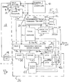
- Fig. 3 there is shown in greater detail the test system 10 of the invention, specifically the Pattern Generator 12 and the Pin Electronics 16 associated with one pin of the test system 10. Also shown is a controller 40 coupled at least to the Test Buffer 42 and the Array 18, the Array 18 being shown in greater detail as a Programmable Driver Command Decoder 18b and a Programmable Receiver Command Decoder 18c.
- the controller 40 in a presently preferred embodiment of the invention is a data processor known in the art as a PS/2 processor manufactured by International Business Machines Corporation. It should be realized however that a number of suitable controlling devices could be so employed.
- the controller 40 is coupled via a suitable interface at least to the aforementioned Test Buffer 42 and Array 18 for storing data therein for specifying the various test cycles and the pin state for each test cycle.
- the interface may take the form of address and data multiplexers for providing the Controller 40 with access to these programmable elements.
- the Test Buffer 42 includes a 1M X 36 bit DRAM block that feeds into a 36 bit wide FIFO prefetch buffer.
- the Test Buffer 42 may further include memory-associated support circuitry such as Error Detection and Correction logic, data and address buffers, DRAM refresh control logic and similar conventional circuitry.
- Controller 40 writes test vector information into the Test Buffer 42 before a test and reads test-related failure information from the Buffer 42 after the test, the failure information being provided from an Error Log 44 as will be described. Controller 40 also writes appropriate data to the Array 18 for specifying pin conditions for the test.
- the Pattern Processor 14 also includes data format circuitry for formatting 32 bits of DRAM output into a sequentially provided series of test words from one to four bits in width, thus employing for each test cycle up to N of the bits. The remaining 4 bits of the 36 bits of DRAM data form a CONTROL signal and are used to control the above mentioned format circuitry.
- the Test Buffer 42 provides 32 bits of stored information to the Pattern Processor 14 and also provides four bits of associated CONTROL information.
- the 32 bits represents a minimum of eight test cycles, each test cycle thus having four bits for specifying test conditions.
- the CONTROL input to the pattern processor 14 specifies up to 16 different decodings of the 32 bit input.
- the CONTROL input may specify a code of 016 to indicate that the 32 bits are to be divided into eight test cycles, each test cycle being represented by four bits.
- the state of the M bits may reflect the state of the corresponding N bits of the 32 bit input.
- a code of 116 may indicate that the 32 bits represent 16 test cycles having two bits per cycle.
- the Pattern Processor 14 provides two variable and two fixed bits as the M bits. Further by example another code indicates that algorithmic pattern generation is in effect and that the 32 bits are to be considered as algorithmic instructions. That is, for algorithmic processing the 32 bits are differentiated into fields with one field specifying, by example, a pin state and another field specifying a number of loops or iterations to be executed with the test pin applying the specified pin state.
- the bits 12a are appended to (M-N) fixed bits, where the number of output bits (M) determines the total number of states (2 M ) that are available at any one pin to test the DUT.
- M the number of output bits (M) determines the total number of states (2 M ) that are available at any one pin to test the DUT.
- M the number of output bits (M) determines the total number of states (2 M ) that are available at any one pin to test the DUT.
- M equals four for specifying during a test sequence up to 16 different pin states.
- the programmable timing generator 20 provides a number of timing pulses whose position can be altered in response to control signals.
- the programmable timing generator 20 includes several sources of timing pulses each having an output line buffered by a multiplexor whose inputs are connected to each of the sources while the select signals are connected to the control lines. In this manner the change of the control line status shifts the output pulses to new positions.
- Another alternative to changing the timing position is to directly couple the control lines from the command decodes to the timing generators.
- the Array 18 is comprised of two sections, specifically the Programmable Driver Command Decoder 18b and the Programmable Receiver Command Decoder 18c. Decoder 18b is employed to decode the M-bit control word from pattern processor 14 to control pin driver functions while Decoder 18c decodes the same M-bit control word to control receiver functions.
- Array 18 is a high speed RAM device where the M-bit control word is used as the address input. The width of the RAM is such that all necessary signals for controlling all pin-related functions are produced simultaneously and in parallel as the control word 18a.
- the depth of the RAM is less than or equal to 2 M and determines the maximum number of states that can be programmed for any one pin during a single test. As was stated, in the presently preferred embodiment the depth is 16 words.
- the Decoder 18b outputs are divided into two groups.
- a first group is applied to Timing Generator 20 and controls timing edge selection for driver pulse start and stop, and also a time at which to switch to a third driver state.
- a second group of Decoder 18b outputs drives the Format and Driver Status Control Logic 24.
- the information that is conveyed by this second group of output lines determines the format (RZ, NRZ, DNRZ, R1, etc.), the type of data (1,0) and whether the driver is on (drive one or drive zero) or in a third state.
- the Receive Logic block 26 of Fig. 2 is indicated in dashed outline and can be seen to include a number of components.
- the Programmable Receiver Command Decoder 18c is similar in structure to the Programmable Driver Command Decoder 18b described above but instead operates to control the status of the Receivers 46a and 46b, determine the timing to be applied to received data latches 48a and 46b, generate the expected data from the DUT for comparison with the actual DUT output by comparator 50, select a type of test (level, 'glitch' or receivers off), define a time window for a 'glitch' or transient detector 52, as well through a select multiplexer 54 to select a mode of error detection and to inhibit error logging if the pin is used as a drive pin only during a current cycle.
- a type of test level, 'glitch' or receivers off
- the type of receiver preferred for the test system 10 is a high gain differential amplifier wherein the signal from the DUT is connected to a positive input and a reference voltage is connected to a negative input.
- the output of the amplifier is essentially a binary output (i.e. either a high or a low output). In this manner whenever the DUT output exceeds the reference voltage the output is high and when the DUT input falls below the reference the output is low.
- a minimum number of Receivers 46a and 46b for an efficient test of bidirectional-type drivers is two. However, it is within the scope of the invention to provide more than two receivers if simultaneous testing of several parameters is desired. Also, under most test conditions the receiver 46a and 46b reference voltage can remain at fixed levels. However, it is within the scope of the invention to couple Digital to Analog Converters (DACs) 46c and 46d between the Programmable Receiver Command Decoder 18c and the Receivers 46a and 46b.
- the DACs 46c and 46d have a plurality of digital inputs coupled to a corresponding portion of the control word 18a for specifying, on a per cycle basis, the magnitude of each DAC output voltage and thus the magnitude of the associated receiver reference level.
- the teaching of the invention readily accommodates the additional functionality by simply increasing the width of the memory used for receiver decoding to generate the required additional receiver control lines.
- Latches 48a and 48b capture the output state of the associated receiver 46a and 46b, respectively, at a desired strobe time. After the receiver data is captured there is sufficient time to compare in Comparator 50 the DUT signal with the expected data generated by the Programmable Receiver Command Decoder 18c. The position of the strobe is controlled by the Timing Generator 20 in response to a control signal that forms a part of the control word 18a generated by the Programmable Receiver Command Decoder 18c.
- the Glitch Detector 52 is employed to detect any switching activity within a predefined time window.
- the Glitch Detector 52 has an input coupled to the Timing Generator 20 and operates as follows. At the beginning of the window the status of each of the receivers 46a and 46b is latched. For the duration of the window the latched receiver output is compared to a time dependent output of the Receivers 46a and 46b by means of an Exclusive-Or logic function. The output of the Exclusive-Or function is employed to drive a gated set input of a set-reset latch. This gate is enabled for the duration of the window. At the end of the test cycle the status of the latch is tested and subsequently reset. If the set-reset latch is found to be set it is indicated that there occurred an excursion of the DUT signal from the state as captured at the beginning of the time window.
- the Receiver 26 includes a Digital Delay 56 that imposes a predetermined delay on the M bit address input to the Programmable Receiver Command Decoder 18c.
- the receiver portion of the command word 18a is generated later in time than the driver portion of the command word 18a.
- the length of the delay time imposed by Digital Delay 26 is selected to compensate for signal propagation delays between the DUT and the pin electronics. In that the round trip signal propagation delay may be approximately six nanoseconds, for a typical DUT-Pin electronics spacing, while the test cycle time at 250 MHZ is only four nanoseconds, the Digital Delay 56 operates to maintain signals returned from the DUT in synchronism with the test timing.
- the Error Log 44 provides a mechanism for recording the occurrence of a test cycle producing an error, that is, recording during which test cycle(s) the DUT output deviated from a predicted output.
- Error Log 44 includes a RAM having an address that is incremented on every cycle and a corresponding RAM location written with the output of the Select Multiplexer 54. Alternately, additional logic is provided for incrementing and writing the RAM only when an error condition is indicated. The Error Log 44 contents are subsequently transferred to the memory in Test Buffer 42 and read out by the Controller 40 for off-line analysis to determine if a failure is recorded.
- Block 24 performs pin formatting and driver control.
- Block 24 includes a set-reset latch wherein applicable bits of control word 18a gate timing pulses to both the set and reset lines.
- the logic directs a start pulse timing signal to the latch set input and an end pulse timing signal to the latch reset input.
- RZ return to zero
- the Driver 28 includes two time dependent inputs. The first of these inputs determines if the Driver 28 is enabled to respond to the second input or whether the Driver 28 will remain in its third state independent of the state of the second line. The output of the Driver 28 goes to the Receivers 46a and 46b and through the pin to the DUT. In addition to the time dependent signals there are two additional control lines (not shown in Fig. 3) which determine the output high and output low voltage levels. In the presently preferred embodiment of the invention the voltage levels are predefined before the test and remain constant during the test. In other embodiments of the invention however these output high and output low voltage levels are variable on a test cycle by test cycle basis.
- DACs specifically a DAC High Level (DACHL) 28a and a DAC Low Level (DACLL) 28b, are coupled between the Programmable Driver Command Decoder 18b and the Driver 28.
- DACHL DAC High Level
- DACLL DAC Low Level
- Each of the DACs 28a and 28b has a plurality of digital inputs coupled to a corresponding portion of the control word 18a for specifying, on a per cycle basis, the magnitude of the DAC output voltage.
- the teaching of the invention readily accommodates this additional functionality by increasing the width of the RAM used for driver decoding to generate the required additional driver control lines.
- the Pattern Processor 14 reads out the required M bits/pin/cycle sequentially to execute all required test steps.
- this implementation can impose a limitation since embedded memory array testing and LSSD logic testing require a large number of test cycles.
- embedded memory array and similar test patterns are regular in structure, they can be generated algorithmically as described at pages 26-28 in the previously mentioned journal article "250-MHZ Advanced Test Systems", IEEE Design & Test of Computers, 1988 by A. J. Gruodis and D. E. Hoffman.
- LSSD shift registers further requires that some pins have the capability to provide large strings of pseudo-random data. This is a consequence of LSSD design and test generation. Tester pins requiring this capability are those coupled to LSSD Shift Register data In (SRI) and data Out (SRO) pins. For example, if for proper test of the logic X test vectors are required to be applied to the logic, and if the length of the LSSD shift register string is Y, then the SRI and SRO pins will require XY test cycles. Similarly, the LSSD shift clocks A and B require the same amount of data. However, since the clocks are repetitive, they can be generated algorithmically. In general, the same algorithmic capabilities used for address and data generation when testing memory arrays can also be used for generating the LSSD shift clocks.
- SRI LSSD Shift Register data In
- SRO data Out
- the invention provides in a per-pin semiconductor test system, having a plurality of test pins expressed as (P total ), circuitry coupled to each test pin for providing the system with a total possible number of test pin conditions given by (2 M ) P total , wherein M is an integer and is expressive of a number of active interconnects coupled between the test pin pattern generator and the test pin driver/receiver electronics. For example, assuming a pin complement of 1024 the resulting number of specifiable pin conditions is 16104 based on M being equal to four active signal interconnects. For the case described above wherein only one of the M interface lines is active, such as when performing algorithmic testing, the number of specifiable system pin conditions is 2104 ⁇
Landscapes
- Engineering & Computer Science (AREA)
- General Engineering & Computer Science (AREA)
- Physics & Mathematics (AREA)
- General Physics & Mathematics (AREA)
- Tests Of Electronic Circuits (AREA)
Claims (18)
- Gerät zum Steuern einer Operation eines Prüfstifts eines Prüfsystems (10) für Halbleitervorrichtungen, eines Typs, der umfaßt:Ein Mittel (40, 42) zum Speichern und Ausgeben von Informationen betreffend den Zustand eines Prüfstifts jeweils für einzelne einer Vielzahl aufeinanderfolgender Prüfzyklen;ein Mittel (12) mit einem Eingang, der an das Speichermittel (40, 42) gekoppelt ist, zum Generieren von Wörtern an seinem Ausgang für jeden der Prüfzyklen, wobei jedes der Wörter aus M Bits gespeicherter Daten besteht; undein Mittel (16) mit einem Eingang, der an den Ausgang der Generierungsmittel (12) gekoppelt ist, zum Decodieren jedes einzelnen Worts zu einem von 2M Steuerwörtern, die jeweils eine Vielzahl von Steuerbits beinhalten, wobei vorbestimmte der Vielzahl von Steuerbits an das Stift-Treibermittel (28) gekoppelt sind zum Spezifizieren mindestens eines Merkmals eines elektrischen Signals, das zum Prüfstift übertragen wird, für jeden der Prüfzyklen,ein Prüfstiftsignal-Empfangsmittel (30) zum Ankoppeln des Decodiermittels (16) an den Prüfstift, um von diesem ein elektrisches Signal zu empfangen, wobei vorbestimmte der Steuerbits des Decodiermittels (16) an das Stiftempfangsmittel (30) gekoppelt sind, um für jeden der Prüfzyklen mindestens ein Betriebsmerkmal zu spezifizieren, das dem Stiftempfangsmittel (30) zugeordnet ist,dadurch gekennzeichnet, daßdiese Speicher- und Ausgabemittel (40, 42) an diese Wortgenerierungsmittel (12) eine abgespeicherte Information ausgibt, die die elektrischen Merkmale des Prüfstifts für jeden der Vielzahl von Prüfzyklen spezifiziert, und das Speicher- und Ausgabemittel (40, 42) ferner Steuerinformationen ausgibt zum Spezifizieren, wie das Wortgenerierungsmittel (12) die Information interpretieren muß, zum Bestimmen des Status der M Bits für jeden einer Vielzahl von Prüfzyklen.
- Gerät gemäß Anspruch 1, in dem die Steuerinformation spezifiziert, daß die Information zum Bestimmen des Status der M Bits als algorithmische Prüfanweisung zu interpretieren ist.
- Gerät gemäß Anspruch 1 oder 2, in dem die gespeicherte Information, die an das Wortgenerierungsmittel (12) ausgegeben wird, aus 32 Bits besteht, die Steuerinformation aus vier Bits besteht, jedes der aus M Bits bestehenden Wörter generiert wird unter Benutzung von N < M Bits der gespeicherten Information, und wobei M gleich vier Bits ist.
- Gerät gemäß einem beliebigen der Ansprüche 1 bis 3, in dem das charakteristische Merkmal des elektrischen Signals einen logischen Zustandsparameter des elektrischen Signals ausdrückt, wobei dieser Parameter aus der Gruppe gewählt wird, die aus einem logischen Zustand, einem Impulsformat und einer Spannungsgröße besteht.
- Gerät gemäß einem beliebigen der Ansprüche 1 bis 4, in dem weitere vorgegebene der Vielzahl der Steuerbits mit dem Stift-Treibermittel (28) gekoppelt sind, um für jeden der Prüfzyklen zu spezifizieren, ob das Stift-Treibermittel in einem "Ein"-Zustand, einem "Aus"-Zustand oder in einem dritten Zustand steht.
- Gerät gemäß Anspruch 4 oder 5, das ferner umfaßt Digital/ Analog-Wandlermittel (28a, 28b) mit Eingängen, die an vorgegebene der Steuerbits gekoppelt sind, und ferner mit einem variablen Spannungsausgang, der an das Stift-Treibermittel gekoppelt ist.
- Gerät gemäß einem beliebigen der Ansprüche 1 bis 6, in dem das das Prüfstiftsignal empfangende Mittel (30) aus einer ersten Stiftempfängerschaltung und einer zweiten Stiftempfängerschaltung besteht, jede mit einem Eingang, der mit dem Prüfstift gekoppelt ist, und in dem das dem Stiftsignal-Empfangsmittel zugeordnete Betriebsmerkmal eine Größe eines Referenzspannungssignals ist, das an die erste und an die zweite Stiftempfängerschaltung gelegt wird.
- Gerät gemäß Anspruch 7, und weiter enthaltend ein erstes Analog/Digital-Wandlermittel und ein zweites Analog/ Digital-Wandlermittel, jeweils mit Eingängen, die an unterschiedliche, vorgegebene Steuerhits gekoppelt sind, und einen variablen Spannungsausgang, der an eine zugeordnete Stiftempfängerschaltung gekoppelt ist, um an dieselbe das Referenzspannungssignal zu schicken.
- Gerät gemäß einem beliebigen der Ansprüche 1 bis 8, in dem das dem Stiftempfangsmittel zugeordnete Betriebsmerkmal ein vorhergesagter logischer Zustand des Prüfstifts zu einem bestimmten Zeitpunkt im Prüfzyklus ist.
- Gerät gemäß Anspruch 9, weiter enthaltend ein erstes Stiftempfängerverriegelungsmittel (48a) und ein zweites Stiftempfängerverriegelungsmittel (48b), deren jedes einen Dateneingang mit einem Ausgang einer zugeordneten Stiftempfängerschaltung gekoppelt hat, und einen Befehlseingang mit einem Zeittaktgenerierungsmittel (20) gekoppelt hat, zum Verriegeln des Ausgangs der zugeordneten Stiftempfängerschaltung in Übereinstimmung mit dem Befehlseingang.
- Gerät gemäß Anspruch 10, in dem das Takt-generierende Mittel einen Steuereingang aufweist, der an eines bzw. mehrere vorgegebene Steuerbits gekoppelt ist und auf diese zu einem gewünschten Zeitpunkt während des Prüfzyklus mit Generieren eines oder mehrerer Taktsignale reagiert in Übereinstimmung mit Informationen, die durch diesen einen bzw. mehrere Steuerbiteingänge ausgedrückt werden, und in dem das Stiftsignal-Empfangsmittel ferner Mittel zum Erfassen einer Abweichung des empfangenen Stiftsignals von einer vorgegebenen Signalhöhe innerhalb eines vorgegebenen Zeitintervalls beinhaltet, wobei das vorgegebene Zeitintervall durch die Information, die von diesem einen bzw. mehreren an das Taktgenerierungsmittel gekoppelten Steuerbiteingängen ausgedrückt wird, spezifiziert wird.
- Gerät gemäß Anspruch 1, in dem das Decodiermittel ferner Verzögerungsmittel zum Verzögern der Anwendung des Ausgangs der Generierungsmittel zum Decodiermittel zum Kompensieren einer Signalfortpflanzungsverzögerung zwischen dem Prüfstift und einer gerade geprüften Vorrichtung umfaßt, die an den Prüfstift gekoppelt ist.
- Gerät gemäß Anspruch 1, in dem das Halbleitervorrichtungs-Prüfsystem eine Vielzahl von Prüfstiften aufweist, wobei jedem der Prüfstifte jeweils ein Speichermittel, Generierungsmittel und Decodiermittel zugeordnet ist, wobei das Gerät ferner Schnittstellenmittel zum Koppeln eines Eingangs des Speichermittels, Generierungsmittel und Decodiermittel, jeweils den einzelnen Prüfstiften zugeordnet, an Steuermittel umfaßt, wobei die Steuermittel innerhalb der einzelnen Speichermittel, Generierungsmittel und Decodiermittel vor der Durchführung der Vielzahl der Prüfzyklen Informationen speichern zum unabhängigen Spezifizieren einer Operation für jeden der zugeordneten Prüfstifte des Halbleitervorrichtungs-Prüfsystems.
- Ein Verfahren zum Betrieb eins Prüfsystems, das eine Vielzahl von Prüfstiften aufweist, wobei für jeden der Prüfstifte die folgenden Initialisierungsschritte vorgesehen sind:Speichern einer Vielzahl von Prüfmustern und -befehlen innerhalb eines Prüfmuster-Speichermittels (42); undSpeichern einer Vielzahl von ersten Steuerwörtern innerhalb eines ersten Steuerwort-Speichermittels und einer Vielzahl von zweiten Steuerwörtern innerhalb eines zweiten Steuerwort-Speichermittels, wobei die Vielzahl von ersten Steuerwörtern jeweils eine Vielzahl von Bits zum Steuern einer Operation eines Prüfstift-Treibermittels (28), und die Vielzahl von zweiten Steuerwörtern jeweils eine Vielzahl von Bits zum Steuern einer Operation eines Prüfstift-Empfängermittels (30) beinhaltet, wobei jedes der ersten und der zweiten Steuerwort-Speichermittel auf die abgespeicherten Prüfmuster und -befehle mit Ausgeben wenigstens eines der gespeicherten Steuerwörter als entsprechende Reaktion reagiert.
- Ein Verfahren gemäß Anspruch 14, und wobei während der Ausführung einer durch die abgespeicherten Prüfmuster und -befehle definierten Prüfung das Verfahren ferner die folgenden Schritte beinhaltet:Zugreifen auf die Prüfmuster-Speichermittel (42) zum Abrufen von Prüfmuster- und -befehlsdaten in Multiplen von N Bits per Zyklus aus denselben, wobei N eine Variable ist;Legen der abgerufenen Daten auf einen Eingang eines Musterverarbeitungsmittels, so daß ein Prüfmuster mit M Bits je Zyklus an einem Ausgang erzeugt wird, wobei M eine Konstante ist;Legen der M Datenbits auf einen Eingang des ersten Steuerwort-Speichermittels und auf einen Eingang des zweiten Steuerwort-Speichermittels zum Auswählen eines vorher abgespeicherten Steuerworts zum Ausgeben aus denselben, wobei das durch die einzelnen ersten und zweiten Steuerwort-Speichermittel auszugebende Steuerwort eine Vielzahl von Steuerbits aufweist, die größer als M sind; undSteuern einer Operation des Prüfstift--Treibermittels (28) mit den Steuerwörtern, die aus dem ersten Steuerspeichermittel ausgegeben wurden, und Steuern einer Operation des Prüfstift-Empfängermittels (30) mit den Steuerwörtern, die aus dem zweiten Steuerspeichermittel ausgegeben wurden.
- Ein Verfahren gemäß Anspruch 15, in dem N gleich oder kleiner als vier ist und in dem M gleich vier ist.
- Ein Verfahren gemäß Anspruch 15 oder 16, in dem der Steuerschritt den logischen Zustand des Prüfstift-Treibermittels (28), ein Impulsformat des Prüfstift-Treibermittels, eine Spannungsgröße und -polarität des Prüfstift-Treibermittels, und/oder ob das Prüfstift-Treibermittel im "Ein"-Zustand oder im "Aus"-Zustand oder in einem dritten Zustand steht, steuert.
- Ein Verfahren gemäß Anspruch 15 oder 16, in dem der Steuerschritt einen erwarteten logischen Zustand des Prüfstifts zu einem bestimmten Zeitpunkt in einem Prüfzyklus steuert, eine Größe eines dem Prüfstift-Empfängermittel (30) zugeordneten Spannungs-Schwellenwerts steuert, einen Zeitpunkt, zu dem ein Ausgang des Prüfstift-Empfängermittels abgetastet wird, steuert, und/oder die Position eines Zeitfensters steuert, in dem der Ausgang des Prüfstift-Empfängermittels auf Auftreten einer Signalauslenkung geprüft wird, und in dem der Schritt des Legens der Dateneinheit auf einen Eingang des Steuerwort-Speichermittels einen Schritt zur Verzögerung der Anwendung der Dateneinheit zum Kompensieren einer Signallaufzeitverzögerung zwischen dem Prüfstift und einer gerade geprüften Vorrichtung, die an den Prüfstift gekoppelt ist, beinhaltet.
Applications Claiming Priority (2)
| Application Number | Priority Date | Filing Date | Title |
|---|---|---|---|
| US07/464,473 US5127011A (en) | 1990-01-12 | 1990-01-12 | Per-pin integrated circuit test system having n-bit interface |
| US464473 | 1999-12-16 |
Publications (3)
| Publication Number | Publication Date |
|---|---|
| EP0446550A2 EP0446550A2 (de) | 1991-09-18 |
| EP0446550A3 EP0446550A3 (en) | 1992-08-05 |
| EP0446550B1 true EP0446550B1 (de) | 1996-05-08 |
Family
ID=23844077
Family Applications (1)
| Application Number | Title | Priority Date | Filing Date |
|---|---|---|---|
| EP90480190A Expired - Lifetime EP0446550B1 (de) | 1990-01-12 | 1990-11-27 | Schaltungsprüfsystem mit einer Schnittstelle von N-bit pro Stift |
Country Status (4)
| Country | Link |
|---|---|
| US (2) | US5127011A (de) |
| EP (1) | EP0446550B1 (de) |
| JP (1) | JP2650203B2 (de) |
| DE (1) | DE69026928T2 (de) |
Cited By (1)
| Publication number | Priority date | Publication date | Assignee | Title |
|---|---|---|---|---|
| CN109839548A (zh) * | 2017-11-24 | 2019-06-04 | 深圳市科比特航空科技有限公司 | 接口测试方法、装置及系统 |
Families Citing this family (46)
| Publication number | Priority date | Publication date | Assignee | Title |
|---|---|---|---|---|
| US5321701A (en) * | 1990-12-06 | 1994-06-14 | Teradyne, Inc. | Method and apparatus for a minimal memory in-circuit digital tester |
| JPH04218785A (ja) * | 1990-12-19 | 1992-08-10 | Advantest Corp | Ic試験装置 |
| US5285453A (en) * | 1990-12-28 | 1994-02-08 | International Business Machines Corporation | Test pattern generator for testing embedded arrays |
| US5243274A (en) * | 1992-08-07 | 1993-09-07 | Westinghouse Electric Corp. | Asic tester |
| DE4305442C2 (de) * | 1993-02-23 | 1999-08-05 | Hewlett Packard Gmbh | Verfahren und Vorrichtung zum Erzeugen eines Testvektors |
| JP3212423B2 (ja) * | 1993-09-30 | 2001-09-25 | 富士通株式会社 | テストパターン作成装置 |
| JPH07280883A (ja) * | 1994-04-04 | 1995-10-27 | Advantest Corp | 半導体試験装置 |
| US5544107A (en) * | 1994-08-22 | 1996-08-06 | Adaptec, Inc. | Diagnostic data port for a LSI or VLSI integrated circuit |
| FR2733323B1 (fr) * | 1995-04-19 | 1997-05-30 | Schlumberger Ind Sa | Procede et equipement de test automatique en parallele de composants electroniques |
| US5748642A (en) * | 1995-09-25 | 1998-05-05 | Credence Systems Corporation | Parallel processing integrated circuit tester |
| US5717695A (en) * | 1995-12-04 | 1998-02-10 | Silicon Graphics, Inc. | Output pin for selectively outputting one of a plurality of signals internal to a semiconductor chip according to a programmable register for diagnostics |
| US5621739A (en) * | 1996-05-07 | 1997-04-15 | Intel Corporation | Method and apparatus for buffer self-test and characterization |
| US5737512A (en) * | 1996-05-22 | 1998-04-07 | Teradyne, Inc. | Fast vector loading for automatic test equipment |
| FR2753274B1 (fr) * | 1996-09-10 | 1998-11-27 | Sgs Thomson Microelectronics | Circuit comprenant des moyens de test structurel sans plot de test dedie au test |
| JP3313591B2 (ja) * | 1996-10-02 | 2002-08-12 | 株式会社東芝 | 半導体装置、半導体装置の検査方法及び半導体装置の検査装置 |
| US5828985A (en) * | 1996-11-20 | 1998-10-27 | Advantest Corp. | Semiconductor test system |
| US5978942A (en) * | 1996-12-19 | 1999-11-02 | Simd Solutions, Inc. | STAR-I: scalable tester architecture with I-cached SIMD technology |
| US6018814A (en) * | 1997-03-26 | 2000-01-25 | Simd Solutions, Inc. | Star-I: scalable tester architecture with I-cached SIMD technology |
| US5835506A (en) * | 1997-04-29 | 1998-11-10 | Credence Systems Corporation | Single pass doublet mode integrated circuit tester |
| US5905748A (en) * | 1997-05-27 | 1999-05-18 | Uniphase Corporation | Single mode laser and method suitable for use in frequency multiplied |
| JP3833341B2 (ja) * | 1997-05-29 | 2006-10-11 | 株式会社アドバンテスト | Ic試験装置のテストパターン発生回路 |
| US5919270A (en) * | 1997-08-29 | 1999-07-06 | Credence Systems Corporation | Programmable formatter circuit for integrated circuit tester |
| US5951705A (en) * | 1997-10-31 | 1999-09-14 | Credence Systems Corporation | Integrated circuit tester having pattern generator controlled data bus |
| KR100322525B1 (ko) * | 1998-03-23 | 2002-06-22 | 윤종용 | 출력드라이버를공유하는병렬비트테스트회로및이를이용한병렬비트테스트방법 |
| US6324485B1 (en) * | 1999-01-26 | 2001-11-27 | Newmillennia Solutions, Inc. | Application specific automated test equipment system for testing integrated circuit devices in a native environment |
| JP4425367B2 (ja) * | 1999-03-15 | 2010-03-03 | 株式会社アドバンテスト | 遅延デバイス |
| US6377065B1 (en) * | 2000-04-13 | 2002-04-23 | Advantest Corp. | Glitch detection for semiconductor test system |
| JP2001319500A (ja) * | 2000-05-10 | 2001-11-16 | Mitsubishi Electric Corp | 半導体集積回路装置 |
| GB2362473B (en) * | 2000-05-18 | 2002-08-21 | 3Com Corp | On-chip detector of clock glitches |
| AU6964301A (en) * | 2000-06-06 | 2001-12-17 | Igor Anatolievich Abrosimov | High speed protocol memory test head for a memory tester |
| JP2002048844A (ja) * | 2000-07-31 | 2002-02-15 | Ando Electric Co Ltd | 半導体試験装置 |
| US7019511B1 (en) * | 2001-01-05 | 2006-03-28 | Advanced Micro Devices, Inc. | Optical analysis of integrated circuits |
| AU2002255823A1 (en) * | 2001-03-19 | 2002-10-03 | Nptest, Inc. | Test system formatters |
| US7765443B1 (en) | 2001-03-19 | 2010-07-27 | Credence Systems Corporation | Test systems and methods for integrated circuit devices |
| US6865704B2 (en) * | 2001-11-09 | 2005-03-08 | Agilent Technologies, Inc. | Scan multiplexing for increasing the effective scan data exchange rate |
| US6708139B2 (en) * | 2002-04-30 | 2004-03-16 | Agilent Technologies, Inc. | Method and apparatus for measuring the quality of delay test patterns |
| US6822486B1 (en) * | 2003-08-07 | 2004-11-23 | International Business Machines Corporation | Multiplexer methods and apparatus |
| US7130231B2 (en) * | 2004-11-19 | 2006-10-31 | International Business Machines Corporation | Method, apparatus, and computer program product for implementing enhanced DRAM interface checking |
| US7840862B2 (en) * | 2006-02-17 | 2010-11-23 | Mentor Graphics Corporation | Enhanced diagnosis with limited failure cycles |
| US7925949B2 (en) * | 2008-10-15 | 2011-04-12 | Micron Technology, Inc. | Embedded processor |
| JP2010281797A (ja) * | 2009-06-08 | 2010-12-16 | Toshiba Corp | 半導体試験装置およびそれを用いた試験方法 |
| US9201092B2 (en) * | 2010-04-14 | 2015-12-01 | Advantest Corporation | Apparatus and method for testing a plurality of devices under test |
| US10451653B2 (en) * | 2014-12-19 | 2019-10-22 | Teradyne, Inc. | Controlling a per-pin measurement unit |
| US10473717B2 (en) * | 2016-11-09 | 2019-11-12 | Texas Instruments Incorporated | Methods and apparatus for test insertion points |
| CN112086124B (zh) * | 2020-08-31 | 2023-03-31 | 澜智集成电路(苏州)有限公司 | 双倍速率测试模式参数配置方法及存储介质 |
| CN117976028A (zh) * | 2024-02-04 | 2024-05-03 | 皇虎测试科技(深圳)有限公司 | 一种用于内存测试的内存条及其内存测试方法 |
Family Cites Families (21)
| Publication number | Priority date | Publication date | Assignee | Title |
|---|---|---|---|---|
| US3873818A (en) * | 1973-10-29 | 1975-03-25 | Ibm | Electronic tester for testing devices having a high circuit density |
| US4517661A (en) * | 1981-07-16 | 1985-05-14 | International Business Machines Corporation | Programmable chip tester having plural pin unit buffers which each store sufficient test data for independent operations by each pin unit |
| US4450560A (en) * | 1981-10-09 | 1984-05-22 | Teradyne, Inc. | Tester for LSI devices and memory devices |
| US4608706A (en) * | 1983-07-11 | 1986-08-26 | International Business Machines Corporation | High-speed programmable timing generator |
| US4656632A (en) * | 1983-11-25 | 1987-04-07 | Giordano Associates, Inc. | System for automatic testing of circuits and systems |
| US4639919A (en) * | 1983-12-19 | 1987-01-27 | International Business Machines Corporation | Distributed pattern generator |
| US4806852A (en) * | 1984-09-07 | 1989-02-21 | Megatest Corporation | Automatic test system with enhanced performance of timing generators |
| US4688233A (en) * | 1984-11-10 | 1987-08-18 | Nec Corporation | Digital data transmitting device for communication paths of restricted and unrestricted transmission characteristics |
| US4696005A (en) * | 1985-06-03 | 1987-09-22 | International Business Machines Corporation | Apparatus for reducing test data storage requirements for high speed VLSI circuit testing |
| US4682330A (en) * | 1985-10-11 | 1987-07-21 | International Business Machines Corporation | Hierarchical test system architecture |
| US4698800A (en) * | 1985-10-28 | 1987-10-06 | International Business Machines Corporation | Bi-directional transceiver circuit |
| JPS62118272A (ja) * | 1985-11-19 | 1987-05-29 | Ando Electric Co Ltd | パタ−ン発生装置 |
| US4931723A (en) * | 1985-12-18 | 1990-06-05 | Schlumberger Technologies, Inc. | Automatic test system having a "true tester-per-pin" architecture |
| CA1251575A (en) * | 1985-12-18 | 1989-03-21 | A. Keith Jeffrey | Automatic test system having a "true tester-per-pin" architecture |
| US4727312A (en) * | 1985-12-23 | 1988-02-23 | Genrad, Inc. | Circuit tester |
| US4724378A (en) * | 1986-07-22 | 1988-02-09 | Tektronix, Inc. | Calibrated automatic test system |
| US4855681A (en) * | 1987-06-08 | 1989-08-08 | International Business Machines Corporation | Timing generator for generating a multiplicty of timing signals having selectable pulse positions |
| US4928278A (en) * | 1987-08-10 | 1990-05-22 | Nippon Telegraph And Telephone Corporation | IC test system |
| US4875210A (en) * | 1988-01-06 | 1989-10-17 | Teradyne, Inc. | Automatic circuit tester control system |
| JP2609284B2 (ja) * | 1988-05-10 | 1997-05-14 | 株式会社日立製作所 | 分散形タイミング信号発生装置 |
| JP2591071B2 (ja) * | 1988-06-08 | 1997-03-19 | 横河電機株式会社 | Lsiテストシステム |
-
1990
- 1990-01-12 US US07/464,473 patent/US5127011A/en not_active Expired - Fee Related
- 1990-11-07 JP JP2299984A patent/JP2650203B2/ja not_active Expired - Lifetime
- 1990-11-27 DE DE69026928T patent/DE69026928T2/de not_active Expired - Fee Related
- 1990-11-27 EP EP90480190A patent/EP0446550B1/de not_active Expired - Lifetime
-
1992
- 1992-03-05 US US07/846,320 patent/US5381421A/en not_active Expired - Fee Related
Cited By (1)
| Publication number | Priority date | Publication date | Assignee | Title |
|---|---|---|---|---|
| CN109839548A (zh) * | 2017-11-24 | 2019-06-04 | 深圳市科比特航空科技有限公司 | 接口测试方法、装置及系统 |
Also Published As
| Publication number | Publication date |
|---|---|
| US5127011A (en) | 1992-06-30 |
| JP2650203B2 (ja) | 1997-09-03 |
| JPH03221882A (ja) | 1991-09-30 |
| DE69026928T2 (de) | 1996-11-21 |
| EP0446550A2 (de) | 1991-09-18 |
| EP0446550A3 (en) | 1992-08-05 |
| DE69026928D1 (de) | 1996-06-13 |
| US5381421A (en) | 1995-01-10 |
Similar Documents
| Publication | Publication Date | Title |
|---|---|---|
| EP0446550B1 (de) | Schaltungsprüfsystem mit einer Schnittstelle von N-bit pro Stift | |
| EP0161639B1 (de) | Unabhängige Matrixtaktierung | |
| US5212443A (en) | Event sequencer for automatic test equipment | |
| US6753693B2 (en) | Test apparatuses for semiconductor integrated circuits | |
| US4783785A (en) | Method and apparatus for diagnosis of logical circuits | |
| US6243841B1 (en) | Automated test and evaluation sampling system and method | |
| EP0366553B1 (de) | Prüfgerät und -verfahren zur Prüfung eines elektronischen Geräts und Halbleitergerät mit diesem Prüfgerät | |
| US6311300B1 (en) | Semiconductor testing apparatus for testing semiconductor device including built in self test circuit | |
| EP1204876B1 (de) | Billige taktsteuervorrichtung für ein hochgenaues multimodal-halbleiterprüfgerät | |
| US5835506A (en) | Single pass doublet mode integrated circuit tester | |
| US5869983A (en) | Method and apparatus for controlling compensated buffers | |
| KR20010024360A (ko) | 집적회로 테스터용 포맷 민감성 타이밍 교정 | |
| KR20040047612A (ko) | 반도체 기억 장치의 테스트 방법 및 반도체 기억 장치의테스트 회로 | |
| KR100514335B1 (ko) | 다중 주기 발생기를 구비하는 집적 회로 테스터 | |
| KR100599918B1 (ko) | 집적회로 테스터용 프로그램 가능한 포맷 회로 | |
| KR100513406B1 (ko) | 반도체 시험장치 | |
| KR101021375B1 (ko) | 멀티태스킹 알고리즘 패턴 발생기를 갖춘 반도체 테스트시스템 | |
| US7171611B2 (en) | Apparatus for determining the access time and/or the minimally allowable cycle time of a memory | |
| KR100439460B1 (ko) | 반도체 집적 회로 및 동작 방법 | |
| US20030212935A1 (en) | Circuit and method for accelerating the test time of a serial access memory device |
Legal Events
| Date | Code | Title | Description |
|---|---|---|---|
| PUAI | Public reference made under article 153(3) epc to a published international application that has entered the european phase |
Free format text: ORIGINAL CODE: 0009012 |
|
| AK | Designated contracting states |
Kind code of ref document: A2 Designated state(s): DE FR GB |
|
| 17P | Request for examination filed |
Effective date: 19911112 |
|
| PUAL | Search report despatched |
Free format text: ORIGINAL CODE: 0009013 |
|
| AK | Designated contracting states |
Kind code of ref document: A3 Designated state(s): DE FR GB |
|
| 17Q | First examination report despatched |
Effective date: 19941125 |
|
| GRAH | Despatch of communication of intention to grant a patent |
Free format text: ORIGINAL CODE: EPIDOS IGRA |
|
| GRAA | (expected) grant |
Free format text: ORIGINAL CODE: 0009210 |
|
| AK | Designated contracting states |
Kind code of ref document: B1 Designated state(s): DE FR GB |
|
| REF | Corresponds to: |
Ref document number: 69026928 Country of ref document: DE Date of ref document: 19960613 |
|
| ET | Fr: translation filed | ||
| PLBE | No opposition filed within time limit |
Free format text: ORIGINAL CODE: 0009261 |
|
| STAA | Information on the status of an ep patent application or granted ep patent |
Free format text: STATUS: NO OPPOSITION FILED WITHIN TIME LIMIT |
|
| 26N | No opposition filed | ||
| PG25 | Lapsed in a contracting state [announced via postgrant information from national office to epo] |
Ref country code: FR Effective date: 19970731 |
|
| PG25 | Lapsed in a contracting state [announced via postgrant information from national office to epo] |
Ref country code: DE Effective date: 19970801 |
|
| REG | Reference to a national code |
Ref country code: FR Ref legal event code: ST |
|
| PGFP | Annual fee paid to national office [announced via postgrant information from national office to epo] |
Ref country code: GB Payment date: 19971017 Year of fee payment: 8 |
|
| PG25 | Lapsed in a contracting state [announced via postgrant information from national office to epo] |
Ref country code: GB Free format text: LAPSE BECAUSE OF NON-PAYMENT OF DUE FEES Effective date: 19981127 |
|
| GBPC | Gb: european patent ceased through non-payment of renewal fee |
Effective date: 19981127 |