EP0442414A2 - Zusammengesetztes Halbleitersubstrat und Verfahren zu seiner Herstellung - Google Patents
Zusammengesetztes Halbleitersubstrat und Verfahren zu seiner Herstellung Download PDFInfo
- Publication number
- EP0442414A2 EP0442414A2 EP91101865A EP91101865A EP0442414A2 EP 0442414 A2 EP0442414 A2 EP 0442414A2 EP 91101865 A EP91101865 A EP 91101865A EP 91101865 A EP91101865 A EP 91101865A EP 0442414 A2 EP0442414 A2 EP 0442414A2
- Authority
- EP
- European Patent Office
- Prior art keywords
- compound semiconductor
- crystal layer
- gaas
- base
- crystal
- Prior art date
- Legal status (The legal status is an assumption and is not a legal conclusion. Google has not performed a legal analysis and makes no representation as to the accuracy of the status listed.)
- Granted
Links
Images

Classifications
-
- H—ELECTRICITY
- H10—SEMICONDUCTOR DEVICES; ELECTRIC SOLID-STATE DEVICES NOT OTHERWISE PROVIDED FOR
- H10D—INORGANIC ELECTRIC SEMICONDUCTOR DEVICES
- H10D62/00—Semiconductor bodies, or regions thereof, of devices having potential barriers
- H10D62/10—Shapes, relative sizes or dispositions of the regions of the semiconductor bodies; Shapes of the semiconductor bodies
- H10D62/17—Semiconductor regions connected to electrodes not carrying current to be rectified, amplified or switched, e.g. channel regions
-
- H10P14/2911—
-
- H10P14/3418—
-
- H10P14/3421—
Definitions
- the present invention relates to a compound semiconductor substrate and a method of manufacturing the same.
- GaAs is known well as a type of a compound semiconductor.
- the GaAs is made to have a resistivity of 106 ⁇ cm or more, it has semi-insulating characteristics.
- active elements are formed in a semi-insulating GaAs substrate, they are not advantageously required to be electrically isolated from each other using a field insulating film.
- a semi-insulating GaAs single-crystal is conventionally made using a single-crystal manufacturing technique such as an LEC method, and the single-crystal is sliced to manufacture semi-insulating GaAs substrates.
- the semi-insulating GaAs single-crystal is constituted by bonding two types of atoms, a shearing stress acting inside the GaAs single-crystal is stronger than that of a silicon single-crystal, and a dislocation density in the GaAs single-crystal is disadvantageously increased.
- the present invention has been made in consideration of the above problem, and has as its object to provide a compound semiconductor substrate having a low dislocation density and a method of manufacturing the same.
- a compound semiconductor substrate includes, on a compound semiconductor base containing a high-concentration impurity, a high-resistance single-crystal layer consisting of the same compound semiconductor as that of the compound semiconductor base.
- a method of manufacturing the compound semiconductor substrate comprises the step of epitaxially growing the same compound semiconductor as a compound semiconductor base to form a high-resistance single-crystal layer on a major surface of the compound semiconductor base containing a high-concentration impurity.
- a dislocation density can be decreased.
- a high-resistance single-crystal layer having a low dislocation density i.e., a single-crystal layer having semi-insulating characteristics can be formed.
- the high-resistance single-crystal layer is formed in a portion where an active element is to be formed, a compound semiconductor substrate having a low dislocation density and even advantageously having a high-resistance, i.e., semi-insulating characteristics can be obtained.
- a curve I in Fig. 1 indicates a decrease in dislocation density when an impurity is doped in GaAs after a crystal is grown. The decrease in dislocation density typically occurs when an n-type impurity is doped.
- a doping concentration of the impurity at a time when the dislocation density is rapidly decreased is 5 x 1017 cm ⁇ 3 or more. This phenomenon is not limited to the GaAs, and it occurs in a compound semiconductor such as GaP or InP consisting of two elements.
- n-type impurity Silicon or carbon is used as an n-type impurity, and selenium, magnesium or the like is used as a p-type impurity.
- a doping concentration is set to be 5 x 1017 cm ⁇ 3 or more to obtain a compound semiconductor single-crystal having a low dislocation density.
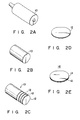
- the present invention is made on the basis of the above phenomenon, n-type GaAs in which a single-crystal, e.g., a silicon element, having a density of 5 x 1017 cm-3 or more is doped as an impurity is grown by an LEC method or an HB method, thereby forming an n-type GaAs single-crystal 10 having a low dislocation density (Fig. 2A).
- the single-crystal 10 is cut (Fig. 2B).
- the cut single-crystal 10 is sliced to obtain an n-type GaAs base 12 (Fig. 2C).
- the base 12 sliced as described above is prospectively used as a substrate for epitaxial growth.
- a high-resistance GaAs single-crystal layer 14 having a resistivity of 106 ⁇ cm is epitaxially grown on the surface of the base 12 (Fig. 2E).
- an amount of impurity contained in GaAs is decreased, or the GaAs is undoped.
- the high-resistance GaAs single-crystal layer 14 is prospectively used as a portion where an active element is to be formed.
- a compound semiconductor substrate 16 according to the present invention is finished by the above method.
- a dislocation density of a single-crystal layer which is epitaxially grown is generally lower than that of a substrate on which the single-crystal layer is grown.
- the dislocation density of the n-type GaAs base 12 is decreased by doping an impurity, and the dislocation density of the GaAs single-crystal layer 14 grown on the base 12 is further decreased.
- a dislocation density is about 50,000 cm ⁇ 2 at a portion where an active element is to be formed.
- the dislocation density of the GaAs single-crystal layer 14 where an active element is to be formed can be set to be 100 cm ⁇ 2 or less.
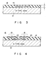
- Fig. 3 is a partially enlarged sectional view showing the GaAs substrate 16 shown in Fig. 2E
- Fig. 4 is a sectional view showing a condition wherein an active element is formed on the GaAs substrate 16.
- the GaAs single-crystal layer 14 which is undoped to have a high-resistance is stacked on the n-type GaAs base 12 by epitaxial growth.
- the high-resistance GaAs single-crystal layer 14 is a layer where an active element 18 is prospectively formed, and an active region 20 prospectively serving as a source, a drain, and a channel of the active element 18 is formed on the single-crystal layer 14.
- the high-resistance GaAs single-crystal layer 14 is formed to have a resistivity of 106 ⁇ cm or more, a field insulating film for isolating the active elements 18 from each other need not be formed (the high-resistance GaAs single-crystal layer 14 has semi-insulating characteristics).
- the high-resistance GaAs single-crystal layer 14 is epitaxially grown on the n-type GaAs base 12 having a low dislocation density, the dislocation density of the single-crystal layer 14 is also low.
- the active elements 18 formed on the GaAs single-crystal layer 14 having a low dislocation density have excellent characteristics, and variations in characteristics of all the active elements 18 can be decreased.
- the variations in characteristics of the active elements 18 can be decreased, in all cases wherein an IC/LSI is formed and wherein an individual semiconductor device is formed, the performance of the IC/LSI and the individual semiconductor device can be improved, and a yield of the products can be improved.
- a thickness t of the high-resistance GaAs single-crystal layer 14 is required to be a minimum thickness required for forming the active region 20.
- the thickness t of the high-resistance GaAs single-crystal layer 14 is set to be about 500 nm or more, it can sufficiently cope with formation of the active region 20.
- a method of growing a crystal at an atomic layer level such as MBE, MOCVD, or MOMBE is preferably used from the viewpoint of improvements of a film quality and controllability of the film thickness t .
- the base 12 contains an impurity to have a low dislocation density.
- the single-crystal layer 14 stacked thereon is undoped to have a high resistance so as to have semi-insulating characteristics.
- an impurity having an effect of decreasing the dislocation density of the base 12 carbon, selenium, magnesium, or the like is used in addition to silicon.
- the dislocation density of the single-crystal can be decreased.
Landscapes
- Engineering & Computer Science (AREA)
- Recrystallisation Techniques (AREA)
- Microelectronics & Electronic Packaging (AREA)
- Physics & Mathematics (AREA)
- Condensed Matter Physics & Semiconductors (AREA)
- General Physics & Mathematics (AREA)
- Manufacturing & Machinery (AREA)
- Computer Hardware Design (AREA)
- Power Engineering (AREA)
- Materials Engineering (AREA)
- Chemical & Material Sciences (AREA)
- Element Separation (AREA)
- Physical Deposition Of Substances That Are Components Of Semiconductor Devices (AREA)
Applications Claiming Priority (2)
| Application Number | Priority Date | Filing Date | Title |
|---|---|---|---|
| JP2032697A JPH0831409B2 (ja) | 1990-02-14 | 1990-02-14 | 化合物半導体装置およびその製造方法 |
| JP32697/90 | 1990-02-14 |
Publications (3)
| Publication Number | Publication Date |
|---|---|
| EP0442414A2 true EP0442414A2 (de) | 1991-08-21 |
| EP0442414A3 EP0442414A3 (en) | 1991-10-23 |
| EP0442414B1 EP0442414B1 (de) | 1996-04-24 |
Family
ID=12366045
Family Applications (1)
| Application Number | Title | Priority Date | Filing Date |
|---|---|---|---|
| EP91101865A Expired - Lifetime EP0442414B1 (de) | 1990-02-14 | 1991-02-11 | Zusammengesetztes Halbleitersubstrat und Verfahren zu seiner Herstellung |
Country Status (5)
| Country | Link |
|---|---|
| US (1) | US5599389A (de) |
| EP (1) | EP0442414B1 (de) |
| JP (1) | JPH0831409B2 (de) |
| KR (1) | KR910016060A (de) |
| DE (1) | DE69118941T2 (de) |
Families Citing this family (22)
| Publication number | Priority date | Publication date | Assignee | Title |
|---|---|---|---|---|
| JP3171807B2 (ja) | 1997-01-24 | 2001-06-04 | 東京エレクトロン株式会社 | 洗浄装置及び洗浄方法 |
| US6815790B2 (en) * | 2003-01-10 | 2004-11-09 | Rapiscan, Inc. | Position sensing detector for the detection of light within two dimensions |
| US8035183B2 (en) * | 2003-05-05 | 2011-10-11 | Udt Sensors, Inc. | Photodiodes with PN junction on both front and back sides |
| US7057254B2 (en) * | 2003-05-05 | 2006-06-06 | Udt Sensors, Inc. | Front illuminated back side contact thin wafer detectors |
| US8120023B2 (en) * | 2006-06-05 | 2012-02-21 | Udt Sensors, Inc. | Low crosstalk, front-side illuminated, back-side contact photodiode array |
| US7256470B2 (en) * | 2005-03-16 | 2007-08-14 | Udt Sensors, Inc. | Photodiode with controlled current leakage |
| US7655999B2 (en) | 2006-09-15 | 2010-02-02 | Udt Sensors, Inc. | High density photodiodes |
| US7242069B2 (en) * | 2003-05-05 | 2007-07-10 | Udt Sensors, Inc. | Thin wafer detectors with improved radiation damage and crosstalk characteristics |
| US7279731B1 (en) * | 2006-05-15 | 2007-10-09 | Udt Sensors, Inc. | Edge illuminated photodiodes |
| US8164151B2 (en) * | 2007-05-07 | 2012-04-24 | Osi Optoelectronics, Inc. | Thin active layer fishbone photodiode and method of manufacturing the same |
| US7656001B2 (en) | 2006-11-01 | 2010-02-02 | Udt Sensors, Inc. | Front-side illuminated, back-side contact double-sided PN-junction photodiode arrays |
| US8519503B2 (en) * | 2006-06-05 | 2013-08-27 | Osi Optoelectronics, Inc. | High speed backside illuminated, front side contact photodiode array |
| US7880258B2 (en) * | 2003-05-05 | 2011-02-01 | Udt Sensors, Inc. | Thin wafer detectors with improved radiation damage and crosstalk characteristics |
| US7709921B2 (en) * | 2008-08-27 | 2010-05-04 | Udt Sensors, Inc. | Photodiode and photodiode array with improved performance characteristics |
| US7576369B2 (en) * | 2005-10-25 | 2009-08-18 | Udt Sensors, Inc. | Deep diffused thin photodiodes |
| US8686529B2 (en) * | 2010-01-19 | 2014-04-01 | Osi Optoelectronics, Inc. | Wavelength sensitive sensor photodiodes |
| US9178092B2 (en) | 2006-11-01 | 2015-11-03 | Osi Optoelectronics, Inc. | Front-side illuminated, back-side contact double-sided PN-junction photodiode arrays |
| US20100053802A1 (en) * | 2008-08-27 | 2010-03-04 | Masaki Yamashita | Low Power Disk-Drive Motor Driver |
| MX2011002852A (es) | 2008-09-15 | 2011-08-17 | Udt Sensors Inc | Fotodiodo de espina de capa activa delgada con una capa n+ superficial y metodo para fabricacion del mismo. |
| WO2010084878A1 (ja) * | 2009-01-20 | 2010-07-29 | 住友電気工業株式会社 | 導電性GaAsの結晶と基板およびそれらの作製方法 |
| US8399909B2 (en) * | 2009-05-12 | 2013-03-19 | Osi Optoelectronics, Inc. | Tetra-lateral position sensing detector |
| US8912615B2 (en) | 2013-01-24 | 2014-12-16 | Osi Optoelectronics, Inc. | Shallow junction photodiode for detecting short wavelength light |
Family Cites Families (14)
| Publication number | Priority date | Publication date | Assignee | Title |
|---|---|---|---|---|
| JPS53110973A (en) * | 1977-03-10 | 1978-09-28 | Futaba Denshi Kogyo Kk | Method and apparatus for manufacturing compounds |
| JPS54106169A (en) * | 1978-02-08 | 1979-08-20 | Nec Corp | Vapor epitaxial growth device |
| GB2030551B (en) * | 1978-09-22 | 1982-08-04 | Philips Electronic Associated | Growing a gaas layer doped with s se or te |
| JPS5591816A (en) * | 1978-12-29 | 1980-07-11 | Fujitsu Ltd | Manufacturing of semiconductor device |
| JPS5627972A (en) * | 1979-08-17 | 1981-03-18 | Oki Electric Ind Co Ltd | Manufacture of compound semiconductor device |
| JPS59184570A (ja) * | 1983-04-01 | 1984-10-19 | Matsushita Electric Ind Co Ltd | 電界効果トランジスタ |
| US4632710A (en) * | 1983-05-10 | 1986-12-30 | Raytheon Company | Vapor phase epitaxial growth of carbon doped layers of Group III-V materials |
| GB2156579B (en) * | 1984-03-15 | 1987-05-07 | Standard Telephones Cables Ltd | Field effect transistors |
| JPS613465A (ja) * | 1984-06-18 | 1986-01-09 | Fujitsu Ltd | 半導体装置及びその製造方法 |
| DE3682959D1 (de) * | 1985-06-21 | 1992-01-30 | Matsushita Electric Industrial Co Ltd | Bipolarer transistor mit heterouebergang und verfahren zu seiner herstellung. |
| JPH0670973B2 (ja) * | 1985-09-18 | 1994-09-07 | 住友電気工業株式会社 | 化合物半導体のエピタキシヤルウエハ |
| JP2504782B2 (ja) * | 1987-09-25 | 1996-06-05 | 住友電気工業株式会社 | 電界効果トランジスタの製造方法 |
| JPH01179411A (ja) * | 1988-01-08 | 1989-07-17 | Nec Corp | 3−5族化合物半導体気相成長方法 |
| US4935381A (en) * | 1988-12-09 | 1990-06-19 | The Aerospace Corporation | Process for growing GaAs epitaxial layers |
-
1990
- 1990-02-14 JP JP2032697A patent/JPH0831409B2/ja not_active Expired - Fee Related
-
1991
- 1991-02-07 KR KR1019910002056A patent/KR910016060A/ko not_active Ceased
- 1991-02-11 DE DE69118941T patent/DE69118941T2/de not_active Expired - Fee Related
- 1991-02-11 EP EP91101865A patent/EP0442414B1/de not_active Expired - Lifetime
-
1994
- 1994-11-14 US US08/340,478 patent/US5599389A/en not_active Expired - Fee Related
Also Published As
| Publication number | Publication date |
|---|---|
| US5599389A (en) | 1997-02-04 |
| KR910016060A (ko) | 1991-09-30 |
| EP0442414A3 (en) | 1991-10-23 |
| DE69118941D1 (de) | 1996-05-30 |
| EP0442414B1 (de) | 1996-04-24 |
| JPH0831409B2 (ja) | 1996-03-27 |
| JPH03236218A (ja) | 1991-10-22 |
| DE69118941T2 (de) | 1996-09-26 |
Similar Documents
| Publication | Publication Date | Title |
|---|---|---|
| EP0442414A2 (de) | Zusammengesetztes Halbleitersubstrat und Verfahren zu seiner Herstellung | |
| US5311055A (en) | Trenched bipolar transistor structures | |
| EP0447327B1 (de) | Heterostruktur-Halbleiteranordnung | |
| EP0097772B1 (de) | Struktur mit monokristallinem Substrat als Träger für eine Halbleiterschicht für eine Anordnung | |
| US5256550A (en) | Fabricating a semiconductor device with strained Si1-x Gex layer | |
| US20170236924A1 (en) | Superlattice lateral bipolar junction transistor | |
| JPH0766366A (ja) | 半導体積層構造体およびそれを用いた半導体装置 | |
| US5331186A (en) | Heterojunction bipolar transistor with base electrode having Schottky barrier contact to the emitter | |
| JPH07176541A (ja) | ヘテロ接合バイポーラトランジスタ | |
| US6580104B1 (en) | Elimination of contaminants prior to epitaxy and related structure | |
| JP3024584B2 (ja) | 半導体装置の製造方法 | |
| US4837178A (en) | Method for producing a semiconductor integrated circuit having an improved isolation structure | |
| WO2001037349A1 (en) | Vertical heterojunction bipolar transistor | |
| US4939102A (en) | Method of growing III-V semiconductor layers with high effective hole concentration | |
| EP0327122B1 (de) | Komplementäre bipolar Halbleiteranordnung | |
| US5183776A (en) | Heteroepitaxy by growth of thermally strained homojunction superlattice buffer layers | |
| US6043143A (en) | Ohmic contact and method of manufacture | |
| JP2828980B2 (ja) | 半導体結晶の製造方法 | |
| US5453398A (en) | Method for fabricating quantum wire laser diode | |
| CA1315018C (en) | P-type buffer layers for integrated circuits | |
| JPH0969625A (ja) | 電界効果トランジスタ | |
| JPS61123175A (ja) | ヘテロ接合パイポ−ラトランジスタの製造方法 | |
| JPH05335327A (ja) | ヘテロ接合バイポーラトランジスタ | |
| JPH01283943A (ja) | 化合物半導体集積回路およびその製造方法 | |
| JPH0974103A (ja) | 半導体素子およびその製造方法 |
Legal Events
| Date | Code | Title | Description |
|---|---|---|---|
| PUAI | Public reference made under article 153(3) epc to a published international application that has entered the european phase |
Free format text: ORIGINAL CODE: 0009012 |
|
| 17P | Request for examination filed |
Effective date: 19910211 |
|
| AK | Designated contracting states |
Kind code of ref document: A2 Designated state(s): DE FR GB |
|
| PUAL | Search report despatched |
Free format text: ORIGINAL CODE: 0009013 |
|
| RHK1 | Main classification (correction) |
Ipc: C30B 29/40 |
|
| AK | Designated contracting states |
Kind code of ref document: A3 Designated state(s): DE FR GB |
|
| 17Q | First examination report despatched |
Effective date: 19940202 |
|
| GRAA | (expected) grant |
Free format text: ORIGINAL CODE: 0009210 |
|
| AK | Designated contracting states |
Kind code of ref document: B1 Designated state(s): DE FR GB |
|
| REF | Corresponds to: |
Ref document number: 69118941 Country of ref document: DE Date of ref document: 19960530 |
|
| ET | Fr: translation filed | ||
| GRAH | Despatch of communication of intention to grant a patent |
Free format text: ORIGINAL CODE: EPIDOS IGRA |
|
| PLBE | No opposition filed within time limit |
Free format text: ORIGINAL CODE: 0009261 |
|
| STAA | Information on the status of an ep patent application or granted ep patent |
Free format text: STATUS: NO OPPOSITION FILED WITHIN TIME LIMIT |
|
| 26N | No opposition filed | ||
| REG | Reference to a national code |
Ref country code: GB Ref legal event code: 746 Effective date: 19981007 |
|
| REG | Reference to a national code |
Ref country code: FR Ref legal event code: D6 |
|
| REG | Reference to a national code |
Ref country code: GB Ref legal event code: IF02 |
|
| PGFP | Annual fee paid to national office [announced via postgrant information from national office to epo] |
Ref country code: GB Payment date: 20060208 Year of fee payment: 16 |
|
| PGFP | Annual fee paid to national office [announced via postgrant information from national office to epo] |
Ref country code: DE Payment date: 20060209 Year of fee payment: 16 |
|
| PGFP | Annual fee paid to national office [announced via postgrant information from national office to epo] |
Ref country code: FR Payment date: 20060220 Year of fee payment: 16 |
|
| GBPC | Gb: european patent ceased through non-payment of renewal fee |
Effective date: 20070211 |
|
| REG | Reference to a national code |
Ref country code: FR Ref legal event code: ST Effective date: 20071030 |
|
| PG25 | Lapsed in a contracting state [announced via postgrant information from national office to epo] |
Ref country code: DE Free format text: LAPSE BECAUSE OF NON-PAYMENT OF DUE FEES Effective date: 20070901 |
|
| PG25 | Lapsed in a contracting state [announced via postgrant information from national office to epo] |
Ref country code: GB Free format text: LAPSE BECAUSE OF NON-PAYMENT OF DUE FEES Effective date: 20070211 Ref country code: FR Free format text: LAPSE BECAUSE OF NON-PAYMENT OF DUE FEES Effective date: 20070228 |