EP0442414A2 - Compound semiconductor substrate and method of manufacturing the same - Google Patents
Compound semiconductor substrate and method of manufacturing the same Download PDFInfo
- Publication number
- EP0442414A2 EP0442414A2 EP91101865A EP91101865A EP0442414A2 EP 0442414 A2 EP0442414 A2 EP 0442414A2 EP 91101865 A EP91101865 A EP 91101865A EP 91101865 A EP91101865 A EP 91101865A EP 0442414 A2 EP0442414 A2 EP 0442414A2
- Authority
- EP
- European Patent Office
- Prior art keywords
- compound semiconductor
- crystal layer
- gaas
- base
- crystal
- Prior art date
- Legal status (The legal status is an assumption and is not a legal conclusion. Google has not performed a legal analysis and makes no representation as to the accuracy of the status listed.)
- Granted
Links
- 239000004065 semiconductor Substances 0.000 title claims abstract description 47
- 150000001875 compounds Chemical class 0.000 title claims abstract description 42
- 239000000758 substrate Substances 0.000 title claims abstract description 31
- 238000004519 manufacturing process Methods 0.000 title claims description 9
- 239000013078 crystal Substances 0.000 claims abstract description 54
- 239000012535 impurity Substances 0.000 claims abstract description 23
- 229910001218 Gallium arsenide Inorganic materials 0.000 claims description 41
- 238000000034 method Methods 0.000 claims description 9
- XUIMIQQOPSSXEZ-UHFFFAOYSA-N Silicon Chemical compound [Si] XUIMIQQOPSSXEZ-UHFFFAOYSA-N 0.000 claims description 5
- 229910052710 silicon Inorganic materials 0.000 claims description 5
- 239000010703 silicon Substances 0.000 claims description 5
- FYYHWMGAXLPEAU-UHFFFAOYSA-N Magnesium Chemical compound [Mg] FYYHWMGAXLPEAU-UHFFFAOYSA-N 0.000 claims description 3
- BUGBHKTXTAQXES-UHFFFAOYSA-N Selenium Chemical compound [Se] BUGBHKTXTAQXES-UHFFFAOYSA-N 0.000 claims description 3
- 229910052749 magnesium Inorganic materials 0.000 claims description 3
- 239000011777 magnesium Substances 0.000 claims description 3
- 229910052711 selenium Inorganic materials 0.000 claims description 3
- 239000011669 selenium Substances 0.000 claims description 3
- 238000002488 metal-organic chemical vapour deposition Methods 0.000 claims description 2
- 238000001741 metal-organic molecular beam epitaxy Methods 0.000 claims description 2
- 238000001451 molecular beam epitaxy Methods 0.000 claims description 2
- 230000003247 decreasing effect Effects 0.000 description 9
- OKTJSMMVPCPJKN-UHFFFAOYSA-N Carbon Chemical compound [C] OKTJSMMVPCPJKN-UHFFFAOYSA-N 0.000 description 2
- 229910052799 carbon Inorganic materials 0.000 description 2
- 230000000694 effects Effects 0.000 description 2
- 238000010008 shearing Methods 0.000 description 2
- 230000015572 biosynthetic process Effects 0.000 description 1
- 238000005498 polishing Methods 0.000 description 1
- 239000000126 substance Substances 0.000 description 1
Images

Classifications
-
- H—ELECTRICITY
- H01—ELECTRIC ELEMENTS
- H01L—SEMICONDUCTOR DEVICES NOT COVERED BY CLASS H10
- H01L21/00—Processes or apparatus adapted for the manufacture or treatment of semiconductor or solid state devices or of parts thereof
- H01L21/70—Manufacture or treatment of devices consisting of a plurality of solid state components formed in or on a common substrate or of parts thereof; Manufacture of integrated circuit devices or of parts thereof
- H01L21/77—Manufacture or treatment of devices consisting of a plurality of solid state components or integrated circuits formed in, or on, a common substrate
- H01L21/78—Manufacture or treatment of devices consisting of a plurality of solid state components or integrated circuits formed in, or on, a common substrate with subsequent division of the substrate into plural individual devices
- H01L21/782—Manufacture or treatment of devices consisting of a plurality of solid state components or integrated circuits formed in, or on, a common substrate with subsequent division of the substrate into plural individual devices to produce devices, each consisting of a single circuit element
- H01L21/784—Manufacture or treatment of devices consisting of a plurality of solid state components or integrated circuits formed in, or on, a common substrate with subsequent division of the substrate into plural individual devices to produce devices, each consisting of a single circuit element the substrate being a semiconductor body
-
- H—ELECTRICITY
- H01—ELECTRIC ELEMENTS
- H01L—SEMICONDUCTOR DEVICES NOT COVERED BY CLASS H10
- H01L29/00—Semiconductor devices specially adapted for rectifying, amplifying, oscillating or switching and having potential barriers; Capacitors or resistors having potential barriers, e.g. a PN-junction depletion layer or carrier concentration layer; Details of semiconductor bodies or of electrodes thereof ; Multistep manufacturing processes therefor
- H01L29/02—Semiconductor bodies ; Multistep manufacturing processes therefor
- H01L29/06—Semiconductor bodies ; Multistep manufacturing processes therefor characterised by their shape; characterised by the shapes, relative sizes, or dispositions of the semiconductor regions ; characterised by the concentration or distribution of impurities within semiconductor regions
- H01L29/10—Semiconductor bodies ; Multistep manufacturing processes therefor characterised by their shape; characterised by the shapes, relative sizes, or dispositions of the semiconductor regions ; characterised by the concentration or distribution of impurities within semiconductor regions with semiconductor regions connected to an electrode not carrying current to be rectified, amplified or switched and such electrode being part of a semiconductor device which comprises three or more electrodes
-
- H—ELECTRICITY
- H01—ELECTRIC ELEMENTS
- H01L—SEMICONDUCTOR DEVICES NOT COVERED BY CLASS H10
- H01L21/00—Processes or apparatus adapted for the manufacture or treatment of semiconductor or solid state devices or of parts thereof
- H01L21/02—Manufacture or treatment of semiconductor devices or of parts thereof
- H01L21/02104—Forming layers
- H01L21/02365—Forming inorganic semiconducting materials on a substrate
- H01L21/02367—Substrates
- H01L21/0237—Materials
- H01L21/02387—Group 13/15 materials
- H01L21/02395—Arsenides
-
- H—ELECTRICITY
- H01—ELECTRIC ELEMENTS
- H01L—SEMICONDUCTOR DEVICES NOT COVERED BY CLASS H10
- H01L21/00—Processes or apparatus adapted for the manufacture or treatment of semiconductor or solid state devices or of parts thereof
- H01L21/02—Manufacture or treatment of semiconductor devices or of parts thereof
- H01L21/02104—Forming layers
- H01L21/02365—Forming inorganic semiconducting materials on a substrate
- H01L21/02518—Deposited layers
- H01L21/02521—Materials
- H01L21/02538—Group 13/15 materials
- H01L21/02543—Phosphides
-
- H—ELECTRICITY
- H01—ELECTRIC ELEMENTS
- H01L—SEMICONDUCTOR DEVICES NOT COVERED BY CLASS H10
- H01L21/00—Processes or apparatus adapted for the manufacture or treatment of semiconductor or solid state devices or of parts thereof
- H01L21/02—Manufacture or treatment of semiconductor devices or of parts thereof
- H01L21/02104—Forming layers
- H01L21/02365—Forming inorganic semiconducting materials on a substrate
- H01L21/02518—Deposited layers
- H01L21/02521—Materials
- H01L21/02538—Group 13/15 materials
- H01L21/02546—Arsenides
Definitions
- the present invention relates to a compound semiconductor substrate and a method of manufacturing the same.
- GaAs is known well as a type of a compound semiconductor.
- the GaAs is made to have a resistivity of 106 ⁇ cm or more, it has semi-insulating characteristics.
- active elements are formed in a semi-insulating GaAs substrate, they are not advantageously required to be electrically isolated from each other using a field insulating film.
- a semi-insulating GaAs single-crystal is conventionally made using a single-crystal manufacturing technique such as an LEC method, and the single-crystal is sliced to manufacture semi-insulating GaAs substrates.
- the semi-insulating GaAs single-crystal is constituted by bonding two types of atoms, a shearing stress acting inside the GaAs single-crystal is stronger than that of a silicon single-crystal, and a dislocation density in the GaAs single-crystal is disadvantageously increased.
- the present invention has been made in consideration of the above problem, and has as its object to provide a compound semiconductor substrate having a low dislocation density and a method of manufacturing the same.
- a compound semiconductor substrate includes, on a compound semiconductor base containing a high-concentration impurity, a high-resistance single-crystal layer consisting of the same compound semiconductor as that of the compound semiconductor base.
- a method of manufacturing the compound semiconductor substrate comprises the step of epitaxially growing the same compound semiconductor as a compound semiconductor base to form a high-resistance single-crystal layer on a major surface of the compound semiconductor base containing a high-concentration impurity.
- a dislocation density can be decreased.
- a high-resistance single-crystal layer having a low dislocation density i.e., a single-crystal layer having semi-insulating characteristics can be formed.
- the high-resistance single-crystal layer is formed in a portion where an active element is to be formed, a compound semiconductor substrate having a low dislocation density and even advantageously having a high-resistance, i.e., semi-insulating characteristics can be obtained.
- a curve I in Fig. 1 indicates a decrease in dislocation density when an impurity is doped in GaAs after a crystal is grown. The decrease in dislocation density typically occurs when an n-type impurity is doped.
- a doping concentration of the impurity at a time when the dislocation density is rapidly decreased is 5 x 1017 cm ⁇ 3 or more. This phenomenon is not limited to the GaAs, and it occurs in a compound semiconductor such as GaP or InP consisting of two elements.
- n-type impurity Silicon or carbon is used as an n-type impurity, and selenium, magnesium or the like is used as a p-type impurity.
- a doping concentration is set to be 5 x 1017 cm ⁇ 3 or more to obtain a compound semiconductor single-crystal having a low dislocation density.
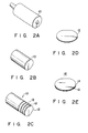
- the present invention is made on the basis of the above phenomenon, n-type GaAs in which a single-crystal, e.g., a silicon element, having a density of 5 x 1017 cm-3 or more is doped as an impurity is grown by an LEC method or an HB method, thereby forming an n-type GaAs single-crystal 10 having a low dislocation density (Fig. 2A).
- the single-crystal 10 is cut (Fig. 2B).
- the cut single-crystal 10 is sliced to obtain an n-type GaAs base 12 (Fig. 2C).
- the base 12 sliced as described above is prospectively used as a substrate for epitaxial growth.
- a high-resistance GaAs single-crystal layer 14 having a resistivity of 106 ⁇ cm is epitaxially grown on the surface of the base 12 (Fig. 2E).
- an amount of impurity contained in GaAs is decreased, or the GaAs is undoped.
- the high-resistance GaAs single-crystal layer 14 is prospectively used as a portion where an active element is to be formed.
- a compound semiconductor substrate 16 according to the present invention is finished by the above method.
- a dislocation density of a single-crystal layer which is epitaxially grown is generally lower than that of a substrate on which the single-crystal layer is grown.
- the dislocation density of the n-type GaAs base 12 is decreased by doping an impurity, and the dislocation density of the GaAs single-crystal layer 14 grown on the base 12 is further decreased.
- a dislocation density is about 50,000 cm ⁇ 2 at a portion where an active element is to be formed.
- the dislocation density of the GaAs single-crystal layer 14 where an active element is to be formed can be set to be 100 cm ⁇ 2 or less.
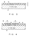
- Fig. 3 is a partially enlarged sectional view showing the GaAs substrate 16 shown in Fig. 2E
- Fig. 4 is a sectional view showing a condition wherein an active element is formed on the GaAs substrate 16.
- the GaAs single-crystal layer 14 which is undoped to have a high-resistance is stacked on the n-type GaAs base 12 by epitaxial growth.
- the high-resistance GaAs single-crystal layer 14 is a layer where an active element 18 is prospectively formed, and an active region 20 prospectively serving as a source, a drain, and a channel of the active element 18 is formed on the single-crystal layer 14.
- the high-resistance GaAs single-crystal layer 14 is formed to have a resistivity of 106 ⁇ cm or more, a field insulating film for isolating the active elements 18 from each other need not be formed (the high-resistance GaAs single-crystal layer 14 has semi-insulating characteristics).
- the high-resistance GaAs single-crystal layer 14 is epitaxially grown on the n-type GaAs base 12 having a low dislocation density, the dislocation density of the single-crystal layer 14 is also low.
- the active elements 18 formed on the GaAs single-crystal layer 14 having a low dislocation density have excellent characteristics, and variations in characteristics of all the active elements 18 can be decreased.
- the variations in characteristics of the active elements 18 can be decreased, in all cases wherein an IC/LSI is formed and wherein an individual semiconductor device is formed, the performance of the IC/LSI and the individual semiconductor device can be improved, and a yield of the products can be improved.
- a thickness t of the high-resistance GaAs single-crystal layer 14 is required to be a minimum thickness required for forming the active region 20.
- the thickness t of the high-resistance GaAs single-crystal layer 14 is set to be about 500 nm or more, it can sufficiently cope with formation of the active region 20.
- a method of growing a crystal at an atomic layer level such as MBE, MOCVD, or MOMBE is preferably used from the viewpoint of improvements of a film quality and controllability of the film thickness t .
- the base 12 contains an impurity to have a low dislocation density.
- the single-crystal layer 14 stacked thereon is undoped to have a high resistance so as to have semi-insulating characteristics.
- an impurity having an effect of decreasing the dislocation density of the base 12 carbon, selenium, magnesium, or the like is used in addition to silicon.
- the dislocation density of the single-crystal can be decreased.
Landscapes
- Engineering & Computer Science (AREA)
- Microelectronics & Electronic Packaging (AREA)
- Power Engineering (AREA)
- General Physics & Mathematics (AREA)
- Computer Hardware Design (AREA)
- Physics & Mathematics (AREA)
- Condensed Matter Physics & Semiconductors (AREA)
- Manufacturing & Machinery (AREA)
- Chemical & Material Sciences (AREA)
- Materials Engineering (AREA)
- Ceramic Engineering (AREA)
- Recrystallisation Techniques (AREA)
- Element Separation (AREA)
- Physical Deposition Of Substances That Are Components Of Semiconductor Devices (AREA)
Abstract
Description
- The present invention relates to a compound semiconductor substrate and a method of manufacturing the same.
- GaAs is known well as a type of a compound semiconductor. When the GaAs is made to have a resistivity of 10⁶ Ω·cm or more, it has semi-insulating characteristics. When active elements are formed in a semi-insulating GaAs substrate, they are not advantageously required to be electrically isolated from each other using a field insulating film. In order to obtain this advantage, a semi-insulating GaAs single-crystal is conventionally made using a single-crystal manufacturing technique such as an LEC method, and the single-crystal is sliced to manufacture semi-insulating GaAs substrates.
- Since the semi-insulating GaAs single-crystal is constituted by bonding two types of atoms, a shearing stress acting inside the GaAs single-crystal is stronger than that of a silicon single-crystal, and a dislocation density in the GaAs single-crystal is disadvantageously increased.
- The present invention has been made in consideration of the above problem, and has as its object to provide a compound semiconductor substrate having a low dislocation density and a method of manufacturing the same.
- The above object can be achieved by the following arrangement.
- According to the present invention, a compound semiconductor substrate includes, on a compound semiconductor base containing a high-concentration impurity, a high-resistance single-crystal layer consisting of the same compound semiconductor as that of the compound semiconductor base.
- According to the present invention, a method of manufacturing the compound semiconductor substrate comprises the step of epitaxially growing the same compound semiconductor as a compound semiconductor base to form a high-resistance single-crystal layer on a major surface of the compound semiconductor base containing a high-concentration impurity.
- According to the compound semiconductor substrate and the method of manufacturing the same, since a high-concentration impurity is contained in the compound semiconductor base, a dislocation density can be decreased. When the same semiconductor as that of the compound semiconductor base is epitaxially grown on the compound semiconductor base having a low dislocation density, a high-resistance single-crystal layer having a low dislocation density, i.e., a single-crystal layer having semi-insulating characteristics can be formed. When the high-resistance single-crystal layer is formed in a portion where an active element is to be formed, a compound semiconductor substrate having a low dislocation density and even advantageously having a high-resistance, i.e., semi-insulating characteristics can be obtained.
- This invention can be more fully understood from the following detailed description when taken in conjunction with the accompanying drawings, in which:
- Fig. 1 is a graph showing a relationship between an impurity concentration and a dislocation density;
- Figs. 2A to 2E are perspective views showing a compound semiconductor substrate according to the embodiment of the present invention in the order of manufacturing steps;
- Fig. 3 is a partially enlarged sectional view showing the compound semiconductor substrate in Fig. 2E; and
- Fig. 4 is a sectional view showing a condition wherein an active element is formed in the compound semiconductor substrate in Fig. 3.
- An embodiment of the present invention will be described below with reference to the accompanying drawings.
- As a method of relieving a shearing stress, a phenomenon wherein an impurity is doped in a single-crystal to decrease a dislocation density in the single-crystal is known. A curve I in Fig. 1 indicates a decrease in dislocation density when an impurity is doped in GaAs after a crystal is grown. The decrease in dislocation density typically occurs when an n-type impurity is doped. As is indicated by the curve I in Fig. 1, a doping concentration of the impurity at a time when the dislocation density is rapidly decreased is 5 x 10¹⁷ cm⁻³ or more. This phenomenon is not limited to the GaAs, and it occurs in a compound semiconductor such as GaP or InP consisting of two elements. Silicon or carbon is used as an n-type impurity, and selenium, magnesium or the like is used as a p-type impurity. When the n- or p-type impurity is used, a doping concentration is set to be 5 x 10¹⁷ cm⁻³ or more to obtain a compound semiconductor single-crystal having a low dislocation density.
- The present invention is made on the basis of the above phenomenon, n-type GaAs in which a single-crystal, e.g., a silicon element, having a density of 5 x 10¹⁷ cm-³ or more is doped as an impurity is grown by an LEC method or an HB method, thereby forming an n-type GaAs single-
crystal 10 having a low dislocation density (Fig. 2A). The single-crystal 10 is cut (Fig. 2B). The cut single-crystal 10 is sliced to obtain an n-type GaAs base 12 (Fig. 2C). Thebase 12 sliced as described above is prospectively used as a substrate for epitaxial growth. Mirror polishing is performed on the surface of thebase 12, and thebase 12 is washed by a chemical treatment to clean its mirror surface (Fig. 2D). A high-resistance GaAs single-crystal layer 14 having a resistivity of 10⁶ Ω·cm is epitaxially grown on the surface of the base 12 (Fig. 2E). In order to form the single-crystal layer 14 having a resistivity of 10⁶ Ω·cm or more, an amount of impurity contained in GaAs is decreased, or the GaAs is undoped. The high-resistance GaAs single-crystal layer 14 is prospectively used as a portion where an active element is to be formed. - A
compound semiconductor substrate 16 according to the present invention is finished by the above method. - A dislocation density of a single-crystal layer which is epitaxially grown is generally lower than that of a substrate on which the single-crystal layer is grown. In the
GaAs substrate 16 with the above arrangement, the dislocation density of the n-type GaAs base 12 is decreased by doping an impurity, and the dislocation density of the GaAs single-crystal layer 14 grown on thebase 12 is further decreased. At present, in a GaAs substrate consisting of an undoped GaAs single-crystal, a dislocation density is about 50,000 cm⁻² at a portion where an active element is to be formed. In the GaAssubstrate 16 according to the present invention, the dislocation density of the GaAs single-crystal layer 14 where an active element is to be formed can be set to be 100 cm⁻² or less. - Fig. 3 is a partially enlarged sectional view showing the
GaAs substrate 16 shown in Fig. 2E, and Fig. 4 is a sectional view showing a condition wherein an active element is formed on theGaAs substrate 16. - As shown in Fig. 3, the GaAs single-
crystal layer 14 which is undoped to have a high-resistance is stacked on the n-type GaAs base 12 by epitaxial growth. The high-resistance GaAs single-crystal layer 14 is a layer where anactive element 18 is prospectively formed, and anactive region 20 prospectively serving as a source, a drain, and a channel of theactive element 18 is formed on the single-crystal layer 14. Since the high-resistance GaAs single-crystal layer 14 is formed to have a resistivity of 10⁶ Ω·cm or more, a field insulating film for isolating theactive elements 18 from each other need not be formed (the high-resistance GaAs single-crystal layer 14 has semi-insulating characteristics). In addition, since the high-resistance GaAs single-crystal layer 14 is epitaxially grown on the n-type GaAs base 12 having a low dislocation density, the dislocation density of the single-crystal layer 14 is also low. Theactive elements 18 formed on the GaAs single-crystal layer 14 having a low dislocation density have excellent characteristics, and variations in characteristics of all theactive elements 18 can be decreased. Since the variations in characteristics of theactive elements 18 can be decreased, in all cases wherein an IC/LSI is formed and wherein an individual semiconductor device is formed, the performance of the IC/LSI and the individual semiconductor device can be improved, and a yield of the products can be improved. - In the
compound semiconductor substrate 16 according to the present invention, a thickness t of the high-resistance GaAs single-crystal layer 14 is required to be a minimum thickness required for forming theactive region 20. For example, at present, when the thickness t of the high-resistance GaAs single-crystal layer 14 is set to be about 500 nm or more, it can sufficiently cope with formation of theactive region 20. When the high-resistance GaAs single-crystal layer 14 is epitaxially grown, a method of growing a crystal at an atomic layer level such as MBE, MOCVD, or MOMBE is preferably used from the viewpoint of improvements of a film quality and controllability of the film thickness t. - This embodiment has been described in the combination of the GaAs
base 12 containing a high-concentration impurity and the GaAs single-crystal layer 14 which is undoped to have a high resistance. However, the same effect as described above can be obtained with the following combinations. - 1) GaP is used as the
base 12, and GaP is used as the single-crystal layer 14. - 2) InP is used as the
base 12, and InP is used as the single-crystal layer 14. - In the above combinations, as in the above embodiment, the base 12 contains an impurity to have a low dislocation density. The single-
crystal layer 14 stacked thereon is undoped to have a high resistance so as to have semi-insulating characteristics. - As an impurity having an effect of decreasing the dislocation density of the
base 12, carbon, selenium, magnesium, or the like is used in addition to silicon. When any of these impurities is doped not only in a GaAs single-crystal but also in a GaP or InP single-crystal, the dislocation density of the single-crystal can be decreased.
Claims (10)
- A compound semiconductor substrate characterized by comprising:
a compound semiconductor base having a major surface and containing a high-concentration impurity; and
a high-resistance single-crystal layer consisting of the same compound semiconductor as that of said compound semiconductor base. - A substrate according to claim 1, characterized in that a concentration of an impurity of said compound semiconductor base is not less than 5 X 10¹⁷ cm⁻³.
- A substrate according to claim 1, characterized in that a resistivity of said high-resistance single-crystal layer is not less than 10¹⁶ Ω·cm.
- A substrate according to claim 1, characterized in that said high-resistance single-crystal layer is an undoped layer.
- A substrate according to claim 1, characterized in that said high-resistance single-crystal layer has a thickness of not less than 500 nm.
- A substrate according to claim 1, characterized in that said impurity is an element selected from the group consisting of silicon, selenium, and magnesium.
- A substrate according to claim 1, characterized in that said compound semiconductor is one semiconductor selected from the group consisting of Group III to V compound semiconductors.
- A substrate according to claim 7, characterized in that said Group III to V compound semiconductor is one semiconductor selected from the group consisting of GaAs, GaP, and InP.
- A method of manufacturing a compound semiconductor substrate, comprising the step of epitaxially growing the same compound semiconductor as a compound semiconductor base to form a high-resistance single-crystal layer on a major surface of said compound semiconductor base containing a high-concentration impurity.
- A method according to claim 9, characterized in that the step of epitaxially growing the same compound semiconductor as said compound semiconductor base comprises the step of performing one method selected from the group consisting of MBE, MOCVD, and MOMBE.
Applications Claiming Priority (2)
| Application Number | Priority Date | Filing Date | Title |
|---|---|---|---|
| JP2032697A JPH0831409B2 (en) | 1990-02-14 | 1990-02-14 | Compound semiconductor device and manufacturing method thereof |
| JP32697/90 | 1990-02-14 |
Publications (3)
| Publication Number | Publication Date |
|---|---|
| EP0442414A2 true EP0442414A2 (en) | 1991-08-21 |
| EP0442414A3 EP0442414A3 (en) | 1991-10-23 |
| EP0442414B1 EP0442414B1 (en) | 1996-04-24 |
Family
ID=12366045
Family Applications (1)
| Application Number | Title | Priority Date | Filing Date |
|---|---|---|---|
| EP91101865A Expired - Lifetime EP0442414B1 (en) | 1990-02-14 | 1991-02-11 | Compound semiconductor substrate and method of manufacturing the same |
Country Status (5)
| Country | Link |
|---|---|
| US (1) | US5599389A (en) |
| EP (1) | EP0442414B1 (en) |
| JP (1) | JPH0831409B2 (en) |
| KR (1) | KR910016060A (en) |
| DE (1) | DE69118941T2 (en) |
Families Citing this family (22)
| Publication number | Priority date | Publication date | Assignee | Title |
|---|---|---|---|---|
| JP3171807B2 (en) * | 1997-01-24 | 2001-06-04 | 東京エレクトロン株式会社 | Cleaning device and cleaning method |
| US6815790B2 (en) * | 2003-01-10 | 2004-11-09 | Rapiscan, Inc. | Position sensing detector for the detection of light within two dimensions |
| US7256470B2 (en) * | 2005-03-16 | 2007-08-14 | Udt Sensors, Inc. | Photodiode with controlled current leakage |
| US7057254B2 (en) * | 2003-05-05 | 2006-06-06 | Udt Sensors, Inc. | Front illuminated back side contact thin wafer detectors |
| US7880258B2 (en) * | 2003-05-05 | 2011-02-01 | Udt Sensors, Inc. | Thin wafer detectors with improved radiation damage and crosstalk characteristics |
| US7242069B2 (en) * | 2003-05-05 | 2007-07-10 | Udt Sensors, Inc. | Thin wafer detectors with improved radiation damage and crosstalk characteristics |
| US8519503B2 (en) | 2006-06-05 | 2013-08-27 | Osi Optoelectronics, Inc. | High speed backside illuminated, front side contact photodiode array |
| US7656001B2 (en) * | 2006-11-01 | 2010-02-02 | Udt Sensors, Inc. | Front-side illuminated, back-side contact double-sided PN-junction photodiode arrays |
| US8120023B2 (en) * | 2006-06-05 | 2012-02-21 | Udt Sensors, Inc. | Low crosstalk, front-side illuminated, back-side contact photodiode array |
| US7655999B2 (en) | 2006-09-15 | 2010-02-02 | Udt Sensors, Inc. | High density photodiodes |
| US7576369B2 (en) * | 2005-10-25 | 2009-08-18 | Udt Sensors, Inc. | Deep diffused thin photodiodes |
| US8035183B2 (en) * | 2003-05-05 | 2011-10-11 | Udt Sensors, Inc. | Photodiodes with PN junction on both front and back sides |
| US8686529B2 (en) | 2010-01-19 | 2014-04-01 | Osi Optoelectronics, Inc. | Wavelength sensitive sensor photodiodes |
| US7279731B1 (en) * | 2006-05-15 | 2007-10-09 | Udt Sensors, Inc. | Edge illuminated photodiodes |
| US8164151B2 (en) * | 2007-05-07 | 2012-04-24 | Osi Optoelectronics, Inc. | Thin active layer fishbone photodiode and method of manufacturing the same |
| US7709921B2 (en) | 2008-08-27 | 2010-05-04 | Udt Sensors, Inc. | Photodiode and photodiode array with improved performance characteristics |
| US9178092B2 (en) | 2006-11-01 | 2015-11-03 | Osi Optoelectronics, Inc. | Front-side illuminated, back-side contact double-sided PN-junction photodiode arrays |
| US20100053802A1 (en) * | 2008-08-27 | 2010-03-04 | Masaki Yamashita | Low Power Disk-Drive Motor Driver |
| JP2012503314A (en) * | 2008-09-15 | 2012-02-02 | オーエスアイ.オプトエレクトロニクス.インコーポレイテッド | Thin active layer fishbone photodiode with shallow N + layer and method of manufacturing the same |
| TW201540881A (en) | 2009-01-20 | 2015-11-01 | Sumitomo Electric Industries | Crystal and substrate of conductive GaAs, and method for forming the same |
| US8399909B2 (en) | 2009-05-12 | 2013-03-19 | Osi Optoelectronics, Inc. | Tetra-lateral position sensing detector |
| US8912615B2 (en) | 2013-01-24 | 2014-12-16 | Osi Optoelectronics, Inc. | Shallow junction photodiode for detecting short wavelength light |
Citations (3)
| Publication number | Priority date | Publication date | Assignee | Title |
|---|---|---|---|---|
| JPS544567A (en) * | 1977-06-13 | 1979-01-13 | Nec Corp | Growing apparatus of ion beam crystal |
| JPS6185814A (en) * | 1984-10-03 | 1986-05-01 | Nec Corp | Compound semiconductor crystal wafer |
| JPS61152083A (en) * | 1984-12-25 | 1986-07-10 | Fuji Electric Co Ltd | Radiant ray detecting semiconductor element |
Family Cites Families (14)
| Publication number | Priority date | Publication date | Assignee | Title |
|---|---|---|---|---|
| JPS53110973A (en) * | 1977-03-10 | 1978-09-28 | Futaba Denshi Kogyo Kk | Method and apparatus for manufacturing compounds |
| JPS54106169A (en) * | 1978-02-08 | 1979-08-20 | Nec Corp | Vapor epitaxial growth device |
| GB2030551B (en) * | 1978-09-22 | 1982-08-04 | Philips Electronic Associated | Growing a gaas layer doped with s se or te |
| JPS5591816A (en) * | 1978-12-29 | 1980-07-11 | Fujitsu Ltd | Manufacturing of semiconductor device |
| JPS5627972A (en) * | 1979-08-17 | 1981-03-18 | Oki Electric Ind Co Ltd | Manufacture of compound semiconductor device |
| JPS59184570A (en) * | 1983-04-01 | 1984-10-19 | Matsushita Electric Ind Co Ltd | Field effect transistor |
| US4632710A (en) * | 1983-05-10 | 1986-12-30 | Raytheon Company | Vapor phase epitaxial growth of carbon doped layers of Group III-V materials |
| GB2156579B (en) * | 1984-03-15 | 1987-05-07 | Standard Telephones Cables Ltd | Field effect transistors |
| JPS613465A (en) * | 1984-06-18 | 1986-01-09 | Fujitsu Ltd | Semiconductor device |
| DE3682959D1 (en) * | 1985-06-21 | 1992-01-30 | Matsushita Electric Ind Co Ltd | BIPOLAR TRANSISTOR WITH HETEROUITION AND METHOD FOR THE PRODUCTION THEREOF. |
| JPH0670973B2 (en) * | 1985-09-18 | 1994-09-07 | 住友電気工業株式会社 | Compound semiconductor epitaxial wafer |
| JP2504782B2 (en) * | 1987-09-25 | 1996-06-05 | 住友電気工業株式会社 | Method for manufacturing field effect transistor |
| JPH01179411A (en) * | 1988-01-08 | 1989-07-17 | Nec Corp | Iii-v compound semiconductor vapor growth method |
| US4935381A (en) * | 1988-12-09 | 1990-06-19 | The Aerospace Corporation | Process for growing GaAs epitaxial layers |
-
1990
- 1990-02-14 JP JP2032697A patent/JPH0831409B2/en not_active Expired - Fee Related
-
1991
- 1991-02-07 KR KR1019910002056A patent/KR910016060A/en not_active Application Discontinuation
- 1991-02-11 DE DE69118941T patent/DE69118941T2/en not_active Expired - Fee Related
- 1991-02-11 EP EP91101865A patent/EP0442414B1/en not_active Expired - Lifetime
-
1994
- 1994-11-14 US US08/340,478 patent/US5599389A/en not_active Expired - Fee Related
Patent Citations (3)
| Publication number | Priority date | Publication date | Assignee | Title |
|---|---|---|---|---|
| JPS544567A (en) * | 1977-06-13 | 1979-01-13 | Nec Corp | Growing apparatus of ion beam crystal |
| JPS6185814A (en) * | 1984-10-03 | 1986-05-01 | Nec Corp | Compound semiconductor crystal wafer |
| JPS61152083A (en) * | 1984-12-25 | 1986-07-10 | Fuji Electric Co Ltd | Radiant ray detecting semiconductor element |
Non-Patent Citations (8)
| Title |
|---|
| APPLIED PHYSICS LETTERS. vol. 37, no. 8, October 1980, NEW YORK US pages 734 - 737; S.A. BARNETT et al.: "Growth of high-quality epitaxial GaAs films by sputter deposition" * |
| APPLIED PHYSICS LETTERS. vol. 42, no. 1, January 1983, NEW YORK US pages 66 - 68; J.C.M. HWANG et al.: "Growth of high-purity GaAs layers by molecular beam epitaxy" * |
| APPLIED PHYSICS LETTERS. vol. 42, no. 2, January 1983, NEW YORK US pages 178 - 180; H. TEMKIN et al.: "Undoped, semi-insulating GaAs layers grown by molecular beam epitaxy" * |
| Derwent Publications Ltd.,LONDON,GB,DATABASE WPI Accession No 79-13418B, week 7907 & JP-A-54004567 (NIPPON ELECTRIC K.K.); 13 January 1979 * |
| JOURNAL OF CRYSTAL GROWTH. vol. 100, no. 1/2, February 1990, AMSTERDAM NL pages 5 - 10; Mitsunobu GOTODA et al.: "Characteristics of Carbon incorporation in GaAs grown by gas source molecular beam epitaxy" * |
| MATERIALS LETTERS vol. 5, no. 4, March 1987, AMSTERDAM NL pages 129 - 133; Shoichi OZAWA et al.: "In-doped GaAs substrate assessment for thin film applications" * |
| PATENT ABSTRACTS OF JAPAN vol. 10, no. 259 (E-434) 04 September 1986, & JP-A-61 085814 (NEC CORP.) 01 May 1986, * |
| PATENT ABSTRACTS OF JAPAN vol. 10, no. 352 (E-458) 27 November 1986, & JP-A-61 152083 (FUJI ELECTRIC CO. LTD.) 10 July 1986, * |
Also Published As
| Publication number | Publication date |
|---|---|
| US5599389A (en) | 1997-02-04 |
| DE69118941D1 (en) | 1996-05-30 |
| EP0442414B1 (en) | 1996-04-24 |
| KR910016060A (en) | 1991-09-30 |
| EP0442414A3 (en) | 1991-10-23 |
| JPH03236218A (en) | 1991-10-22 |
| JPH0831409B2 (en) | 1996-03-27 |
| DE69118941T2 (en) | 1996-09-26 |
Similar Documents
| Publication | Publication Date | Title |
|---|---|---|
| EP0442414A2 (en) | Compound semiconductor substrate and method of manufacturing the same | |
| US5311055A (en) | Trenched bipolar transistor structures | |
| EP0447327B1 (en) | Heterostructure semiconductor device | |
| US5659188A (en) | Capped anneal | |
| US5256550A (en) | Fabricating a semiconductor device with strained Si1-x Gex layer | |
| US20170236924A1 (en) | Superlattice lateral bipolar junction transistor | |
| US5557118A (en) | Hetero-junction type bipolar transistor | |
| US5331186A (en) | Heterojunction bipolar transistor with base electrode having Schottky barrier contact to the emitter | |
| US6580104B1 (en) | Elimination of contaminants prior to epitaxy and related structure | |
| JP3024584B2 (en) | Method for manufacturing semiconductor device | |
| JPH0766366A (en) | Semiconductor multilayered structure and semiconductor device using same | |
| US4837178A (en) | Method for producing a semiconductor integrated circuit having an improved isolation structure | |
| WO2001037349A1 (en) | Vertical heterojunction bipolar transistor | |
| US4939102A (en) | Method of growing III-V semiconductor layers with high effective hole concentration | |
| US5183776A (en) | Heteroepitaxy by growth of thermally strained homojunction superlattice buffer layers | |
| US6043143A (en) | Ohmic contact and method of manufacture | |
| JP2828980B2 (en) | Manufacturing method of semiconductor crystal | |
| JP3255423B2 (en) | Method for forming germanium layer | |
| US5453398A (en) | Method for fabricating quantum wire laser diode | |
| CA1315018C (en) | P-type buffer layers for integrated circuits | |
| JPH0969625A (en) | Field-effect transistor | |
| JPS61123175A (en) | Manufacture of hetero-junction bipolar transistor | |
| JPH05335327A (en) | Heterojunction bipolar transistor | |
| JPH01283943A (en) | Compound semiconductor integrated circuit and manufacture thereof | |
| GB2181889A (en) | Improvements relating to bipolar transistors |
Legal Events
| Date | Code | Title | Description |
|---|---|---|---|
| PUAI | Public reference made under article 153(3) epc to a published international application that has entered the european phase |
Free format text: ORIGINAL CODE: 0009012 |
|
| 17P | Request for examination filed |
Effective date: 19910211 |
|
| AK | Designated contracting states |
Kind code of ref document: A2 Designated state(s): DE FR GB |
|
| PUAL | Search report despatched |
Free format text: ORIGINAL CODE: 0009013 |
|
| RHK1 | Main classification (correction) |
Ipc: C30B 29/40 |
|
| AK | Designated contracting states |
Kind code of ref document: A3 Designated state(s): DE FR GB |
|
| 17Q | First examination report despatched |
Effective date: 19940202 |
|
| GRAA | (expected) grant |
Free format text: ORIGINAL CODE: 0009210 |
|
| AK | Designated contracting states |
Kind code of ref document: B1 Designated state(s): DE FR GB |
|
| REF | Corresponds to: |
Ref document number: 69118941 Country of ref document: DE Date of ref document: 19960530 |
|
| ET | Fr: translation filed | ||
| GRAH | Despatch of communication of intention to grant a patent |
Free format text: ORIGINAL CODE: EPIDOS IGRA |
|
| PLBE | No opposition filed within time limit |
Free format text: ORIGINAL CODE: 0009261 |
|
| STAA | Information on the status of an ep patent application or granted ep patent |
Free format text: STATUS: NO OPPOSITION FILED WITHIN TIME LIMIT |
|
| 26N | No opposition filed | ||
| REG | Reference to a national code |
Ref country code: GB Ref legal event code: 746 Effective date: 19981007 |
|
| REG | Reference to a national code |
Ref country code: FR Ref legal event code: D6 |
|
| REG | Reference to a national code |
Ref country code: GB Ref legal event code: IF02 |
|
| PGFP | Annual fee paid to national office [announced via postgrant information from national office to epo] |
Ref country code: GB Payment date: 20060208 Year of fee payment: 16 |
|
| PGFP | Annual fee paid to national office [announced via postgrant information from national office to epo] |
Ref country code: DE Payment date: 20060209 Year of fee payment: 16 |
|
| PGFP | Annual fee paid to national office [announced via postgrant information from national office to epo] |
Ref country code: FR Payment date: 20060220 Year of fee payment: 16 |
|
| GBPC | Gb: european patent ceased through non-payment of renewal fee |
Effective date: 20070211 |
|
| REG | Reference to a national code |
Ref country code: FR Ref legal event code: ST Effective date: 20071030 |
|
| PG25 | Lapsed in a contracting state [announced via postgrant information from national office to epo] |
Ref country code: DE Free format text: LAPSE BECAUSE OF NON-PAYMENT OF DUE FEES Effective date: 20070901 |
|
| PG25 | Lapsed in a contracting state [announced via postgrant information from national office to epo] |
Ref country code: GB Free format text: LAPSE BECAUSE OF NON-PAYMENT OF DUE FEES Effective date: 20070211 Ref country code: FR Free format text: LAPSE BECAUSE OF NON-PAYMENT OF DUE FEES Effective date: 20070228 |