EP0441503B1 - Farbstrahlaufzeichnungskopf, Substrat dafür und Vorrichtung - Google Patents
Farbstrahlaufzeichnungskopf, Substrat dafür und Vorrichtung Download PDFInfo
- Publication number
- EP0441503B1 EP0441503B1 EP91300537A EP91300537A EP0441503B1 EP 0441503 B1 EP0441503 B1 EP 0441503B1 EP 91300537 A EP91300537 A EP 91300537A EP 91300537 A EP91300537 A EP 91300537A EP 0441503 B1 EP0441503 B1 EP 0441503B1
- Authority
- EP
- European Patent Office
- Prior art keywords
- wiring
- electrothermal transducers
- substrate
- layer
- functional devices
- Prior art date
- Legal status (The legal status is an assumption and is not a legal conclusion. Google has not performed a legal analysis and makes no representation as to the accuracy of the status listed.)
- Expired - Lifetime
Links
Images


Classifications
-
- B—PERFORMING OPERATIONS; TRANSPORTING
- B41—PRINTING; LINING MACHINES; TYPEWRITERS; STAMPS
- B41J—TYPEWRITERS; SELECTIVE PRINTING MECHANISMS, i.e. MECHANISMS PRINTING OTHERWISE THAN FROM A FORME; CORRECTION OF TYPOGRAPHICAL ERRORS
- B41J2/00—Typewriters or selective printing mechanisms characterised by the printing or marking process for which they are designed
- B41J2/005—Typewriters or selective printing mechanisms characterised by the printing or marking process for which they are designed characterised by bringing liquid or particles selectively into contact with a printing material
- B41J2/01—Ink jet
- B41J2/135—Nozzles
- B41J2/16—Production of nozzles
- B41J2/1621—Manufacturing processes
- B41J2/164—Manufacturing processes thin film formation
- B41J2/1646—Manufacturing processes thin film formation thin film formation by sputtering
-
- B—PERFORMING OPERATIONS; TRANSPORTING
- B41—PRINTING; LINING MACHINES; TYPEWRITERS; STAMPS
- B41J—TYPEWRITERS; SELECTIVE PRINTING MECHANISMS, i.e. MECHANISMS PRINTING OTHERWISE THAN FROM A FORME; CORRECTION OF TYPOGRAPHICAL ERRORS
- B41J2/00—Typewriters or selective printing mechanisms characterised by the printing or marking process for which they are designed
- B41J2/005—Typewriters or selective printing mechanisms characterised by the printing or marking process for which they are designed characterised by bringing liquid or particles selectively into contact with a printing material
- B41J2/01—Ink jet
- B41J2/135—Nozzles
- B41J2/14—Structure thereof only for on-demand ink jet heads
- B41J2/14016—Structure of bubble jet print heads
- B41J2/14072—Electrical connections, e.g. details on electrodes, connecting the chip to the outside...
-
- B—PERFORMING OPERATIONS; TRANSPORTING
- B41—PRINTING; LINING MACHINES; TYPEWRITERS; STAMPS
- B41J—TYPEWRITERS; SELECTIVE PRINTING MECHANISMS, i.e. MECHANISMS PRINTING OTHERWISE THAN FROM A FORME; CORRECTION OF TYPOGRAPHICAL ERRORS
- B41J2/00—Typewriters or selective printing mechanisms characterised by the printing or marking process for which they are designed
- B41J2/005—Typewriters or selective printing mechanisms characterised by the printing or marking process for which they are designed characterised by bringing liquid or particles selectively into contact with a printing material
- B41J2/01—Ink jet
- B41J2/135—Nozzles
- B41J2/14—Structure thereof only for on-demand ink jet heads
- B41J2/14016—Structure of bubble jet print heads
- B41J2/14088—Structure of heating means
- B41J2/14112—Resistive element
- B41J2/14129—Layer structure
-
- B—PERFORMING OPERATIONS; TRANSPORTING
- B41—PRINTING; LINING MACHINES; TYPEWRITERS; STAMPS
- B41J—TYPEWRITERS; SELECTIVE PRINTING MECHANISMS, i.e. MECHANISMS PRINTING OTHERWISE THAN FROM A FORME; CORRECTION OF TYPOGRAPHICAL ERRORS
- B41J2/00—Typewriters or selective printing mechanisms characterised by the printing or marking process for which they are designed
- B41J2/005—Typewriters or selective printing mechanisms characterised by the printing or marking process for which they are designed characterised by bringing liquid or particles selectively into contact with a printing material
- B41J2/01—Ink jet
- B41J2/135—Nozzles
- B41J2/16—Production of nozzles
- B41J2/1601—Production of bubble jet print heads
- B41J2/1604—Production of bubble jet print heads of the edge shooter type
-
- B—PERFORMING OPERATIONS; TRANSPORTING
- B41—PRINTING; LINING MACHINES; TYPEWRITERS; STAMPS
- B41J—TYPEWRITERS; SELECTIVE PRINTING MECHANISMS, i.e. MECHANISMS PRINTING OTHERWISE THAN FROM A FORME; CORRECTION OF TYPOGRAPHICAL ERRORS
- B41J2/00—Typewriters or selective printing mechanisms characterised by the printing or marking process for which they are designed
- B41J2/005—Typewriters or selective printing mechanisms characterised by the printing or marking process for which they are designed characterised by bringing liquid or particles selectively into contact with a printing material
- B41J2/01—Ink jet
- B41J2/135—Nozzles
- B41J2/16—Production of nozzles
- B41J2/1621—Manufacturing processes
- B41J2/1626—Manufacturing processes etching
- B41J2/1628—Manufacturing processes etching dry etching
-
- B—PERFORMING OPERATIONS; TRANSPORTING
- B41—PRINTING; LINING MACHINES; TYPEWRITERS; STAMPS
- B41J—TYPEWRITERS; SELECTIVE PRINTING MECHANISMS, i.e. MECHANISMS PRINTING OTHERWISE THAN FROM A FORME; CORRECTION OF TYPOGRAPHICAL ERRORS
- B41J2/00—Typewriters or selective printing mechanisms characterised by the printing or marking process for which they are designed
- B41J2/005—Typewriters or selective printing mechanisms characterised by the printing or marking process for which they are designed characterised by bringing liquid or particles selectively into contact with a printing material
- B41J2/01—Ink jet
- B41J2/135—Nozzles
- B41J2/16—Production of nozzles
- B41J2/1621—Manufacturing processes
- B41J2/1626—Manufacturing processes etching
- B41J2/1629—Manufacturing processes etching wet etching
-
- B—PERFORMING OPERATIONS; TRANSPORTING
- B41—PRINTING; LINING MACHINES; TYPEWRITERS; STAMPS
- B41J—TYPEWRITERS; SELECTIVE PRINTING MECHANISMS, i.e. MECHANISMS PRINTING OTHERWISE THAN FROM A FORME; CORRECTION OF TYPOGRAPHICAL ERRORS
- B41J2/00—Typewriters or selective printing mechanisms characterised by the printing or marking process for which they are designed
- B41J2/005—Typewriters or selective printing mechanisms characterised by the printing or marking process for which they are designed characterised by bringing liquid or particles selectively into contact with a printing material
- B41J2/01—Ink jet
- B41J2/135—Nozzles
- B41J2/16—Production of nozzles
- B41J2/1621—Manufacturing processes
- B41J2/1631—Manufacturing processes photolithography
-
- B—PERFORMING OPERATIONS; TRANSPORTING
- B41—PRINTING; LINING MACHINES; TYPEWRITERS; STAMPS
- B41J—TYPEWRITERS; SELECTIVE PRINTING MECHANISMS, i.e. MECHANISMS PRINTING OTHERWISE THAN FROM A FORME; CORRECTION OF TYPOGRAPHICAL ERRORS
- B41J2/00—Typewriters or selective printing mechanisms characterised by the printing or marking process for which they are designed
- B41J2/005—Typewriters or selective printing mechanisms characterised by the printing or marking process for which they are designed characterised by bringing liquid or particles selectively into contact with a printing material
- B41J2/01—Ink jet
- B41J2/135—Nozzles
- B41J2/16—Production of nozzles
- B41J2/1621—Manufacturing processes
- B41J2/164—Manufacturing processes thin film formation
- B41J2/1642—Manufacturing processes thin film formation thin film formation by CVD [chemical vapor deposition]
-
- B—PERFORMING OPERATIONS; TRANSPORTING
- B41—PRINTING; LINING MACHINES; TYPEWRITERS; STAMPS
- B41J—TYPEWRITERS; SELECTIVE PRINTING MECHANISMS, i.e. MECHANISMS PRINTING OTHERWISE THAN FROM A FORME; CORRECTION OF TYPOGRAPHICAL ERRORS
- B41J2/00—Typewriters or selective printing mechanisms characterised by the printing or marking process for which they are designed
- B41J2/005—Typewriters or selective printing mechanisms characterised by the printing or marking process for which they are designed characterised by bringing liquid or particles selectively into contact with a printing material
- B41J2/01—Ink jet
- B41J2/135—Nozzles
- B41J2/14—Structure thereof only for on-demand ink jet heads
- B41J2002/14379—Edge shooter
-
- B—PERFORMING OPERATIONS; TRANSPORTING
- B41—PRINTING; LINING MACHINES; TYPEWRITERS; STAMPS
- B41J—TYPEWRITERS; SELECTIVE PRINTING MECHANISMS, i.e. MECHANISMS PRINTING OTHERWISE THAN FROM A FORME; CORRECTION OF TYPOGRAPHICAL ERRORS
- B41J2202/00—Embodiments of or processes related to ink-jet or thermal heads
- B41J2202/01—Embodiments of or processes related to ink-jet heads
- B41J2202/13—Heads having an integrated circuit
Definitions
- This invention relates to a recording head of an ink jet recording device to be used for printer, video output printer, etc. as the terminal for output of copying machine, facsimile, word processor, host computer, a substrate for said head an ink jet recording device, particularly to an ink jet recording head having an electrothermal transducer for generating thermal energy as the energy to be utilized for discharging ink and a functional device for recording formed on or internally of the same substrate, a substrate for said head and an ink jet recording device.
- a recording head had a constitution, comprising an array of electrothermal transducers formed on a single crystal silicon substrate, functional devices for driving the electrothermal transducers such as a transistor, a diode array, etc. arranged externally of the silicon substrate as the driving circuit of the electrothermal transducers, with connection between the electrothermal transducers and the functional devices such as transistor array, etc. being done with flexible cable or wire bonding.
- Fig. 12 is a schematic sectional view showing a part of the recording head having the construction as described above.
- 901 is a semiconductor substrate comprising a single crystal silicon.
- 902 is the collector region of an N-type semiconductor, 903 the ohmic contact region of an N-type semiconductor with a high impurity concentration, 904 the base region of a P-type semiconductor, 905 the emitter region of an N-type semiconductor with a high impurity concentration, and the bipolar transistor 920 is formed of these.
- 906 is a silicon oxide layer as the heat accumulation layer and the insulating layer, 907 a hafnium boride (HfB2) as the heat-generating resistor layer, 908 an aluminum (Al) electrode, 909 a silicon oxide layer as the protective layer, and the substrate 930 recording head is constituted of all the members as mentioned above.
- 940 becomes the heat generating portion.
- the ceiling plate 910 is bonded to 930, and sectionalizes the liquid channel communicated to the discharge opening 950A in co-operative fashion.
- the substrate for recording head with such constitution (heater board) is connected to functional device arrays such as the array of the heat generating portion (heater) 940 and the array of diodes or transistors for driving this through the matrix wiring portion arranged between these.
- functional device arrays such as the array of the heat generating portion (heater) 940 and the array of diodes or transistors for driving this through the matrix wiring portion arranged between these.
- the substrate for recording head with such constitution (heater board) is connected to an array of the heat-generating portions (heater) 940 and an array of functional devices such as an array of diodes or transistors through a matrix wiring portion arranged between these.
- the functional device array portion is arranged on the heater board gradually departed as the first row, the second row, etc.
- the normal direction voltage of the functional device such as diode or transistor tends to be larger as remote from the heater portion (the substrate temperature becomes lower) depending on the temperature distribution of the heater board, particularly involving the problem that its variance is greater as the temperature of the heater board becomes higher in printing for a long time, etc. to have deleterious effect on printing quality.
- the plurality of electrothermal transducers and the plurality of function elements are structurally formed in the surface of a substrate, or the plurality of electrothermal transducers are mounted on the surface of a substrate in the surface of which the function elements are formed, and the electrothermal transducers are mounted in a form of a laminating structure.
- An object of the present invention is to provide an ink jet recording head which can improve thermal efficiency without damaging the life of the heat energy generating member which generates thermal energy to be utilized for discharging ink.
- Another object of the present invention is to provide an ink jet recording head which can make the substrate having heat energy generating members arranged thereon compact, thereby accomplishing making the ink jet recording head itself compact.
- Still another object of the present invention is to provide an ink jet recording head which can improve printing quality.
- Still another object of the present invention is to provide an ink jet recording device equipped with the ink jet recording head as mentioned above.
- a recording head provided with a plurality of electrothermal transducers for generating thermal energy to be utilized for discharging ink supplied to liquid discharge units of said recording head, and a plurality of functional devices arranged in an array and electrically connected to said electrothermal transducers on and internally of the same substrate, said plurality of electrothermal transducers being arranged in an array in the vicinity of common electrode wiring for said functional devices, characterised in that said plurality of functional devices are arranged in an array extending away from said array of electrothermal transducers in a direction transversely of the arrangement direction of said array of electrothermal transducers within the region provided at the wiring portion including said common electrode wiring and selective electrode wiring for said plurality of electrothermal transducers and said plurality of functional devices, said wiring portion being formed essentially at lower layer, in said transversely extending direction, than the layer where said electrothermal transducers are formed.
- the wiring resistance can be made smaller, and also by making the second layer (upper level) wiring thinner, and the protective layer of the electrothermal transducer (heater) thinner, the heater thermal efficiency can be improved. Also, there occurs no wiring resistance variance on account of film thickness variances of the first layer, the second layer wiring layers.
- the matrix portion and the functional device array portion may be made to have double structures, the heater board size can be made compact, and also the wiring resistance is reduced with compaction. Further, wiring resistance correction is facilitated.
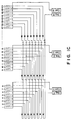
- Fig. 1A shows an example of wiring arrangement on the substrate (silicon substrate) of the ink jet recording device according to an embodiment of the present invention.
- the wiring comprises a first layer wiring which becomes the lower layer wiring, a second layer wiring which becomes the upper layer wiring and a thruhole SH which connects electrically them.
- 1-101 is a common electrode with the first layer wiring, which is connected to the common wiring 1-102.
- the common wiring 1-102 is connected to one of the electrothermal transducers 1-104 juxtaposed laterally in an array through the thruhole via the 1-105 common side take-out wiring with the first layer wiring.
- the electrothermal transducer 1-104 is formed of a heat generating resistance layer and a second wiring, and connected via the segment side take-out wiring 1-105 to the anode electrode 1-106 of the diode 1-113 which is used as the functional device for driving the electrothermal transducer through the thruhole, the second layer wiring, and the thruhole.
- the cathode electrode 1-107 of the diode is connected through the thruhole to the segment lateral wiring 1-108.
- the segment lateral wiring is connected via the thruhole 1-109 to the longitudinal wiring 1-110 with the first layer wiring, and the segment longitudinal wiring to the segment electrode 1-111.
- FIG. 1A an example with a number of 8 segments of the electrotransducers within one block is shown, and particularly those at the both ends are shown in the drawing.
- 8 diodes utilized as the functional devices are juxtaposed in the longitudinal direction in Fig. 1A along the arrangement direction of the segment lateral wiring.
- isolation electrodes 1-112 are arranged around the diodes to form an isolation region.
- the wiring resistance values mutually between the segments are made smaller in difference therebetween by employment of the arrangement as shown in the Figure. More specifically, the wiring resistance depends on the width of the pattern and the total distance wound around of the pattern, and in this embodiment, the common side take-out wiring is from the common electrode is made as thick as possible, and also the wiring resistance between segments is suppressed small by taking sufficiently wide the width of the wiring portion which becomes non-common between segments.
- the wirings from the segment side take-out wiring 1-105 to the diode anode 1-106, and from the segment side thruhole 1-109 to the segment electrode 1-111 may be sometimes restricted in wiring width to tolerate, for example, only 20 ⁇ m or less, and thus are places where wiring resistance is caused to be increased greatly, but by making structurally the arrangement so that the distance wound around may become the same for each segment as the total of the above-mentioned two wirings, it becomes possible to create no great difference mutually between the segments.
- the heater board size becomes smaller and also the wiring becomes shorter, whereby the resistance value becomes smaller.
- the size in the width direction can be made smaller, or the device can be made lengthy by continuous arrangement of the heater boards.
- the protective layer of the heater can be made thin.
- the second layer comprises a double structure of a heater material and a wiring material, but the second layer has the slight portion of the heater portion and the simple shape pattern of the segment wiring, whereby the yield cannot but be lowered by bridge establishment between the wirings. Further, even if the film thicknesses of the first layer, the second layer may be varied respectively, there will occur no variance of wiring resistance for each segment within the block.
- the common electrode 1-101 and the segment electrode 1-111 are selected.
- a pulse for driving passes through the common electrode 1-101 to the common wiring 1-102, the common side take-out wiring 1-103, the electrothermal transducer 1-104, and further through the segment side take-out wiring 1-105 to the anode electrode 1-106 of the diode. Further, passing through the diode, from the diode cathode electrode 1-107, through the segment lateral wiring 108 and the thruhole 1-109, further passing through the segment longitudinal wiring 1-110 and via the segment electrode 1-111, the pulse flows to the external portion.
- the isolation electrode 1-112 is earthed.
- a driving pulse is added to the electrothermal transducer and the resistor generates heat, whereby the ink immediately thereon is heated to be formed, thereby forming discharging ink droplets.
- connection of the electrothermal transducer with the diode as the functional device for driving, and driving of the electrothermal transducer are described in more detail.
- Fig. 1B is a sectional view of the substrate according to the present embodiment with its wiring portion schematically shown.
- the collector base common electrode 12 corresponds to the anode of the diode (1-106 in Fig. 1A), and the emitter electrode 13 to the cathode (1-107 in Fig. 1A).
- V H1 bias of positive potential on the electrothermal transducer connected to the collector base common electrode 12
- the NPN transistor within the cell turns on, and the bias current flows out from the emitter electrode 13 as the collector current and the base current.
- Fig. 1B only two semiconductor functional devices (cells) are shown, but practically such devices correspond to the electrothermal transducers in the number as shown in Fig. 1C to be arranged in the same number and electrically matrix connected so as to be block drivable (see Fig. 1C).
- the common electrodes (com1, ... com8) and selective electrodes (seg1, ... seg8) are arranged alternately on the substrate.
- the group is selected by the switch G1 (the common side switch), and also the electrothermal transducer RH1 is selected by the switch S1 (the segment side switch) to apply a positive voltage V H1 .
- the diode cell SH1 with a transistor constitution is positively biased, whereby a current flows out from the emitter electrode 13.
- the electrothermal transducer RH1 generates heat, which heat energy causes the liquid to undergo a state change and generate bubbles, thereby discharging the liquid through the discharge opening.
- the switch G1 when the electrothermal transducer RH2 is driven, the switch G1, the switch S2 are selectively turned on to drive the diode cell SH2, thereby supplying a current to the electrothermal transducer.
- the substrate 1 is earthed through the isolation regions 3, 6, 9.
- the isolation regions 3, 6, 9 of the respective semiconductor devices are prevented.
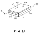
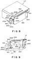
- Fig. 2A is a schematic perspective view of a recording head by use of the substrate constituted as outlined above.
- Such head as shown in the Figure, has a plurality of discharge openings 500, liquid channel wall members 501 comprising a photosensitive resin, etc. for forming the liquid channels communicated to the discharge openings, ceiling plates 502 and ink supplying openings 503.
- the liquid wall member 501 and the ceiling plate 502 can be also integrally formed by utilizing a resin mold material.
- Fig. 2B is a schematic sectional view of the substrate for recording head according to the present embodiment and its wiring portion, namely a sectional view along the line E-E' in Fig. 2A.
- 1 is a P-type silicon substrate, 2 an N-type collector embedding region for constituting a functional device, 3 a P-type isolation embedding region for functional device separation, 4 an N-type epitaxial region, 5 a P-type base region for constituting the functional device, 6 a P-type isolation region for device separation, 7 an N-type collector region for constituting the functional device, 8 a high concentration P-type base region for constituting the device, 9 a high concentration P-type isolation region for device separation, 10 an N-type emitter region for constituting the device, 11 a high density N-type collector region for constituting the device, 12 a collector base common electrode, 13 an emitter electrode, and 14 an isolation electrode.
- NPN transistors SH1, SH2 are formed, and the collector regions 2, 7, 11 are formed so as to surround completely the emitter region 10 and the base regions 5, 8. Also, as the device separation region, the respective cells are surrounded by the P-type isolation embedding region 3, the P-type isolation region 6 and the high concentration P-type isolation region 9 to be electrically separated.
- an SiO2 film 101 by thermal oxidation on the substrate having the driving portion described is provided an SiO2 film 101 by thermal oxidation, and on the heat accumulation layer 102 comprising a silicon oxide film according to the CVD method or the sputtering method, etc. an electrothermal transducer 110 constituted of a heat-generating resistance layer 103 of HfB2, etc. according to the sputtering method and an electrode 104 of Al, etc.
- Heat-generating resistance layers 103 such as HfB2, etc. are also provided between the collector base common electrode 12 and the emitter electrode 13 and the wirings 202 and 201 such as of Al, etc.
- the heat-generating resistance layer there may be employed otherwise Pt, Ta, ZrB2, Ti-W, Ni-Cr, Ta-Al, Ta-Si, Ta-Mo, Ta-W, Ta-Cu, Ta-Ni, Ta-Ni-Al, Ta-Mo-Ni, Ta-W-Ni, Ta-Si-Al, Ta-W-Al-Ni, Ti-Si, W, Ti, Ti-N, Mo, Mo-Si, W-Si, etc.
- a protective layer 105 such as SiO2, etc. according to sputtering or the CVD method
- a protective film 106 such as Ta, etc.
- the SiO2 film forming the heat accumulation layer 102 is provided integrally with the interlayer insulating film between the lowest layer wirings 12, 14 and 201 and 202 as the intermediate wirings.
- the protective layer 105 it is also similarly integrated with the interlayer insulating film between the wirings 201 and 202.
- actuation tests were conducted by block driving the electrothermal transducer.
- eight semiconductors were connected to one segment and currents each of 300 mA (total 2.4 A) were permitted to flow, and other semiconductor diodes could perform good discharging without erroneous actuation.
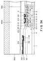
- Fig. 4A is a sectional view of the substrate according to the second embodiment of the present invention.
- the heater board 100a according to the present embodiment may be considered as classified broadly into the three areas A, B, C.
- A is the electrothermal transducer portion
- B the wiring portion
- C the diode portion
- the heat accumulation layer 101 is varied in thickness so as to be adapted to the respective areas.
- the thickness is made about 1.5 to 2.0 ⁇ m in conformity with the heat accumulation layer 102.
- the thickness is made thick, and the at the diode portion C, the thickness is made about 0.3 ⁇ m in view of contact with the first layer wiring 1-102.
- the thickness of the first layer wiring 1-102 has great influence on the wiring resistance of the segment, and therefore made thick up to 0.9 to 1.4 ⁇ m to the extent which does not exceed the thickness of the heat accumulation layer 102 of about 1.0 to 1.5 ⁇ m.
- the second layer wiring 104 has small influence on the wiring resistance, and therefore is made as thin as possible (about 0.3 ⁇ ), whereby the thickness of the protective layer 105 becomes thinner to about 0.4 to 0.6 ⁇ m to improve thermal efficiency to great extent.
- the protective layer 102 in view of the respective layers 104, 105, 106, may be subjected to patterning so that the step difference portion becomes tapered, or the film formation method in which the step difference becomes tapered such as the bias sputtering method may be employed.
- the planer arrangement constitutions of the devices and the wirings are the same as described above in Fig. 1A.
- the wiring resistance has already become smaller in the film constitution of the prior art example, but by taking the constitution of the present embodiment, liberation from the restriction of the antinomy of the prior art is possible, and by varying the film thickness further reduction of wiring resistance and improvement of heat transmission efficiency can be accomplished.
- the wiring can make danger such as short circuit of bridge, etc. or wiring smaller if it is shaped singly so far as possible.
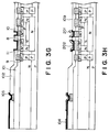
- Fig. 4B shows an embodiment in which the diode arrangement is made as slipped obliquely depending on the pitch of the segment take-out wiring 1-105 in arranging the diodes 1-113 in the longitudinal direction for the embodiment in Fig. 1A.
- the take-out wiring 1-105 becomes linear, whereby the design can be simplified, the wiring resistance reduced and the degree of freedom of the layers upon this improved.
- the anode electrode of 1-106 is performed by the first layer wiring.
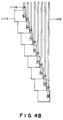
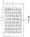
- heater boards with a heater board having a matrix structure of 8 x 8 and 64 heaters as one unit are continuously arranged.
- heaters are arranged with the same pitches as the p-1th unit and the p + 1th unit.
- the common electrode 1-101 and the segment electrode 1-111 are juxtaposed alternately, and at the center of the unit is arranged the isolation electrode 1-112.
- the segment electrode When the constitution as in the embodiment described above is employed concerning the heater board, the segment electrode will not come out, and therefore a plural arrangement of substrates in number of p is also possible with the constitution of m x n matrix as one unit as in the present embodiment.
- Fig. 4D shows an embodiment of the diode 1-113.
- the shape such as the anode electrode 1-106 shown was taken with the second layer wiring, whereby the segment lateral wiring 1-108 became greater in wiring resistance in order to circumvent this portion.
- an opening is provided at the isolation electrode so as to surround the diode to form an anode take-out wiring 1-116, whereby connection to the segment lateral wiring 1-105 is possible with the first layer wiring, while the segment lateral wiring 1-108 of the second layer wiring can be subjected to wiring without any restriction, whereby no increase in wiring resistance will occur.
- taking out of the electrode as in the present embodiment will make the present invention more effective.
- Fig. 5A shows a wiring arrangement embodiment on the substrate (silicon substrate) of an ink jet recording device according to another embodiment of the present invention.
- the wiring comprises a first layer wiring which becomes the lower layer wiring, a second layer wiring which becomes the upper layer wiring, and a thruhole for connecting electrically these.
- 1-101 is the common electrode with the first layer wiring, and connected to the common wiring 1-102.
- the common wiring 1-102 is connected to one of the electrothermal transducers 1-104 juxtaposed laterally in an array through a thruhole via the take-out wiring on the 1-105 common side with the first layer wiring.
- the electrothermal transducer 1-104 is formed of a heat generating resistance layer and the second layer wiring, and via the segment side take-out wiring 1-105 of the first layer wiring, is connected to the anode electrode 1-106 of the diode 1-113 used as the functional device for driving the electrothermal transducer through the thruhole, the second layer wiring, and via the thruhole through the anode electrode 1-106.
- the cathode electrode 1-107 of the diode is connected to the segment lateral wiring 1-108 with the second layer wiring through the thruhole.
- the segment lateral wiring is connected via the thruhole 1-109 to the segment longitudinal wiring 1-110 with the first layer wiring, and the segment longitudinal wiring to the segment electrode 1-111.
- one with the number of electrothermal transducers within one block being made 8 segments is shown by way of example, particularly those at the both ends.
- 8 diodes utilized as the functional device are juxtaposed in the longitudinal direction in Fig. 5A along the arrangement direction of the segment lateral wiring.
- the isolation electrode 1-112 for diode is arranged around the diodes to form an isolation region.
- the diode 1-113 is smaller in size as nearer to the heater 1-104.
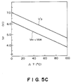
- Fig. 5B the functional description of the means for correcting the thermal influence by changing the diode size is given based on the temperature distribution of the heater board and the temperature characteristics of the diode.
- the heater board 122 is shown with Fig. 5A being omitted, and equipped with the heater row 124 and the diode row 123.
- the heater board 120 is an example in which the individual diode sizes within the diode 121 are made uniform.
- the temperature distribution on A-A' of the heater board 120 is shown in the graph ⁇ I>, and now when the heater is heated, it can be understood that the heater row 124 portion becomes the maximum temperature, and the temperature is lower as departed from that portion.
- ⁇ T D is made the maximum temperature gradient when the heater is heated highest
- T D1 , T D4 , T D8 the maximum temperature differences at the positions of the diodes D1, D4, D8, respectively, namely the temperature differences between when the heater is not heated and when the heater is heated highest.
- D2, D3, D5, D6, D7 the same principle is also applicable to description of D2, D3, D5, D6, D7.
- the diode has smaller V F as the temperature is higher.
- This is applied to the graph ⁇ II> in Fig. 5B, in which the axis of ordinate ⁇ T is set to be of the same scale as in the graph ⁇ I>.
- the heater board 120 becomes to have temperature gradient ⁇ T D
- the temperature at the diode D1 becomes T D1
- V F of the diode D1 becomes V1.
- That of the diode D8 is V8, whereby a V F difference ⁇ V1 ⁇ 8 occurs between the diodes D1 and D8.
- V F of the diodes D1', D4', D8' of the diode row 123 on the heater board 122 are described by referring to the graph ⁇ III>.
- the characteristics of the diodes D1, D4, D8 become respectively V D1 ', V D4 ',V D8 ', which characteristics are made different by varying the diode size utilizing the fact that the voltage drop with the diode becomes greater as the diode size is smaller to increase V F .
- the diode size may be chosen in the manner so that the diodes D1, D4, D8 may be equal in V F at 1/2 of the heater board maximum temperature gradient ⁇ TD, namely T D1 /2, T D4 /2, T D8 /2.
- V F at this time is defined as V o ', and corresponding to V o in the graph ⁇ III>, the actuation points are determined for these in the graph.
- the V F 's of the diodes D1, D4, D8 becomes respectively V1'', V4'', V8'' from the graph ⁇ III>, with the V F difference between the diodes D1 and D8 being ⁇ V1 ⁇ 8''.
- the common electrode 1-101 and the segment electrode 1-111 are chosen.
- the isolation electrode 1-112 is earthed.
- a driving pulse is applied to the electrothermal transducer, whereby the resistor generates heat to heat the ink immediately thereon to effect foaming, thereby forming discharge ink droplets.
- connection of the electrothermal transducer with the diode as the functional device for driving thereof, driving of the electrothermal transducer, etc. are substantially the same as in the first embodiment described above about the preparation steps of the ink jet recording head.
- the constitution of the wiring portion may be also as shown in Fig. 5D. More specifically, in Fig. 5D, a positive bias voltage VH1 is applied on the collector-base electrode 12, and the current from the emitter electrode 13 flows to the electrothermal transducer RH1 or RH2.
- actuation tests were conducted by block driving the electrothermal transducer.
- 8 semiconductor diodes were connected to one segment, and a current of 300 mA (total 2.4 A) was permitted to flow to each diode, and other semiconductors could perform good discharging without erroneous actuation.
- Fig. 6A shows one utilizing different characteristics of the diodes D1 - D8 in Fig. 5B.
- temperature correction was made by designing the diodes so as to have different temperature dependencies, and a diode having the characteristics of V D1 in the graph ⁇ II> with small temperature dependency is placed at D1 nearest to the heater row 124, a diode with higher temperature dependency placed as remote from the heater row 124, until a diode having the characteristic of V D8 is employed as D8.
- V F (kT/q)ln(I F /I S )
- I S qs[D P P n /L P ) + (D n n P )/L n ]
- k, q are constants
- T is temperature
- I F current D p , D n are diffusion constants
- n p , P n are small number carrier densities
- L p , L n are distances to the points where the carrier density becomes 1/e.
- the diodes D1 - D8 may be passed through the diffusion step as required, respectively.
- Fig. 6B shows an embodiment wherein application is changed from the one-dimensional arrangement as described above to the two-dimensional arrangement.
- the temperature distribution by heat generation at the heater row 124 on the heater board 125 is shown by T1 - T5 by the isothermal line representation. Therefore, for obtaining better temperature characteristics, in view of the two-dimensional arrangement, at the line where the temperature becomes the highest as the temperature T1, the diodes D31, D41, D51, D61 are applied, which are subjected to the correction methods in the embodiment 1 and the embodiment 2.
- V F actuation point movement correction or the V F gradient correction is applied more greatly, with correction being weakened as the temperature influence is weaker as T2 to T5, until the correction amount is made the smallest at the outside of the temperature T5 line, namely at the diodes D16, D17, D18, D28, D87, D88, D78. By doing so, V F correction becomes possible at better temperature.
- each diode is shown as Dmn.
- the wiring resistance can be made smaller, and also by making the second layer (upper layer) thinner and the protective layer of the electrothermal transducer thinner, the heater thermal efficiency can be improved without damaging the heater life. Also, there occurs no variance in wiring resistance according to film thickness variance of the first layer, the second layer wiring layers.
- the heater board size can be made compact, and the wiring resistance is also reduced as the size is made more compact. Further, there occurs no cumbersomeness on account of wiring resistance correction.
- the present invention by arranging diodes with different characteristic curves of normal direction saturated voltage for temperature such as making the size the diodes arranged in the region where the temperature on the heater board becomes higher, and the diodes arranged on the region with lower temperature larger, it becomes possible to make the difference in normal direction voltage of the diode according to the temperature distribution on the heater board without increase of the production, which in turn enables improvement of printing quality.
Landscapes
- Engineering & Computer Science (AREA)
- Manufacturing & Machinery (AREA)
- Particle Formation And Scattering Control In Inkjet Printers (AREA)
- Ink Jet (AREA)
- Recording Measured Values (AREA)
Claims (6)
- Ein Substrat für einen Aufzeichnungskopf mit einer Mehrzahl von elektrothermischen Transducern (1-104, 110) zur Erzeugung thermischer Energie, die zum Ausstoßen von Tinte verwendet werden soll, welche Tintenausstoßeinheiten des Aufzeichnungskopfes zugeführt wird, und einer Mehrzahl von funktionalen Vorrichtungen (1-113), die in einer Reihe angeordnet und elektrisch mit den elektrothermischen Transducern auf und innerhalb desselben Substrats verbunden sind, wobei die Mehrzahl von elektrothermischen Transducern (1-104) in einer Reihe in der Nähe einer gemeinsamen Elektrodenverkabelung (1-102) für die funktionalen Vorrichtungen angeordnet sind,
dadurch gekennzeichnet, daß
die Mehrzahl von funktionalen Vorrichtungen (1-113) in einer Reihe angeordnet sind, die sich von der Reihe von elektrothermischen Transducern quer zu der Anordnungsrichtung der Reihe elektrothermischer Transducer innerhalb des Bereiches weg erstreckt, welcher an dem Verkabelungsbereich vorgesehen ist, der die gemeinsame Elektrodenverkabelung (1-102) und die wahlweise Elektrodenverkabelung für die Mehrzahl von elektrothermischen Transducern und die Mehrzahl von funktionalen Vorrichtungen einschließt, wobei der Verkabelungsbereich im wesentlichen an einer Schicht in der sich quer erstreckenden Richtung angeordnet ist, die unterhalb der Schicht liegt, wo die elektrothermischen Transducer ausgebildet sind. - Ein Substrat für einen Aufzeichnungskopf nach Anspruch 1, dadurch gekennzeichnet, daß die Mehrzahl von elektrothermischen Transducern (1-104) und die Merhzahl von funktionalen Vorrichtungen (1-113) in einer bestimmten Anzahl von Blöcken angeordnet sind, und daß die gemeinsame Elektrode (1-101) und die wahlweise Elektrode (1-111) eines jeden Blockes im Wechsel an dem Substrat angeordnet sind.
- Ein Substrat für einen Aufzeichnungskopf nach Anspruch 1 oder 2, dadurch gekennzeichnet, daß die Mehrzahl von funktionalen Vorrichtungen unterschiedliche charakteristischen Kurven gesättigter Spannung über der Temperatur entsprechend dem Abstand von den elektrothermischen Transducern besitzen.
- Ein Substrat für einen Aufzeichnungskopf nach Anspruoh 1, 2 oder 3, dadurch gekennzeichnet, daß die Größe der funktionalen Vorrichtungen mit zunehmendem Abstand von der Reihe von elektrothermischen Transducern größer wird.
- Ein Substrat für einen Aufzeichnungskopf nach Anspruch 3 oder 4, dadurch gekennzeichnet, daß die Temperaturabhängigkeit der funktionalen Vorrichtungen mit zunehmendem Abstand größer gemacht wird.
- Ein Tintenstrahlaufzeichnungskopf mit einer Mehrzahl von Flüssigkeitsausstoßeinheiten, von denen jede eine Ausstoßöffnung (500) besitzt, und einem Substrat, wie in einem der vorangehenden Ansprüche 1 bis 5 beansprucht, dadurch gekennzeichnet, daß die elektrothermischen Transducer verwendet werden, um Tinte auszustoßen, die den Flussigkeitsausstoßeinheiten zugeführt wird.
Priority Applications (2)
| Application Number | Priority Date | Filing Date | Title |
|---|---|---|---|
| EP93202570A EP0579338B1 (de) | 1990-01-25 | 1991-01-24 | Tintenstrahlaufzeichnungskopf, Substrat dafür und Tintenstrahlaufzeichnungsgerät |
| AT91300537T ATE104214T1 (de) | 1990-01-25 | 1991-01-24 | Farbstrahlaufzeichnungskopf, substrat dafuer und vorrichtung. |
Applications Claiming Priority (4)
| Application Number | Priority Date | Filing Date | Title |
|---|---|---|---|
| JP1349090 | 1990-01-25 | ||
| JP1348990 | 1990-01-25 | ||
| JP13489/90 | 1990-01-25 | ||
| JP13490/90 | 1990-01-25 |
Related Child Applications (1)
| Application Number | Title | Priority Date | Filing Date |
|---|---|---|---|
| EP93202570.3 Division-Into | 1993-09-01 |
Publications (3)
| Publication Number | Publication Date |
|---|---|
| EP0441503A2 EP0441503A2 (de) | 1991-08-14 |
| EP0441503A3 EP0441503A3 (en) | 1992-01-08 |
| EP0441503B1 true EP0441503B1 (de) | 1994-04-13 |
Family
ID=26349304
Family Applications (2)
| Application Number | Title | Priority Date | Filing Date |
|---|---|---|---|
| EP91300537A Expired - Lifetime EP0441503B1 (de) | 1990-01-25 | 1991-01-24 | Farbstrahlaufzeichnungskopf, Substrat dafür und Vorrichtung |
| EP93202570A Expired - Lifetime EP0579338B1 (de) | 1990-01-25 | 1991-01-24 | Tintenstrahlaufzeichnungskopf, Substrat dafür und Tintenstrahlaufzeichnungsgerät |
Family Applications After (1)
| Application Number | Title | Priority Date | Filing Date |
|---|---|---|---|
| EP93202570A Expired - Lifetime EP0579338B1 (de) | 1990-01-25 | 1991-01-24 | Tintenstrahlaufzeichnungskopf, Substrat dafür und Tintenstrahlaufzeichnungsgerät |
Country Status (6)
| Country | Link |
|---|---|
| US (2) | US5182577A (de) |
| EP (2) | EP0441503B1 (de) |
| JP (1) | JP2916006B2 (de) |
| AT (1) | ATE158234T1 (de) |
| DE (2) | DE69101648T2 (de) |
| ES (1) | ES2051560T3 (de) |
Families Citing this family (21)
| Publication number | Priority date | Publication date | Assignee | Title |
|---|---|---|---|---|
| ATE158234T1 (de) * | 1990-01-25 | 1997-10-15 | Canon Kk | Tintenstrahlaufzeichnungskopf, substrat dafür und tintenstrahlaufzeichnungsgerät |
| CA2075097C (en) * | 1991-08-02 | 2000-03-28 | Hiroyuki Ishinaga | Recording apparatus, recording head and substrate therefor |
| US5598189A (en) * | 1993-09-07 | 1997-01-28 | Hewlett-Packard Company | Bipolar integrated ink jet printhead driver |
| US5660739A (en) * | 1994-08-26 | 1997-08-26 | Canon Kabushiki Kaisha | Method of producing substrate for ink jet recording head, ink jet recording head and ink jet recording apparatus |
| JPH08118641A (ja) | 1994-10-20 | 1996-05-14 | Canon Inc | インクジェットヘッド、インクジェットヘッドカートリッジ、インクジェット装置およびインクが再注入されたインクジェットヘッドカートリッジ用インク容器 |
| JP3397473B2 (ja) * | 1994-10-21 | 2003-04-14 | キヤノン株式会社 | 液体噴射ヘッド用素子基板を用いた液体噴射ヘッド、該ヘッドを用いた液体噴射装置 |
| JP3413063B2 (ja) | 1996-07-09 | 2003-06-03 | キヤノン株式会社 | 液体吐出方法及び液体吐出ヘッド |
| JP3652016B2 (ja) | 1996-07-12 | 2005-05-25 | キヤノン株式会社 | 液体吐出ヘッドおよび液体吐出方法 |
| US5901425A (en) | 1996-08-27 | 1999-05-11 | Topaz Technologies Inc. | Inkjet print head apparatus |
| JPH11129483A (ja) | 1997-07-03 | 1999-05-18 | Canon Inc | 液体吐出ヘッド用オリフィスプレートの製造方法、オリフィスプレート、該オリフィスプレートを有する液体吐出ヘッド及び液体吐出ヘッドの製造方法 |
| US6494563B2 (en) | 1997-12-25 | 2002-12-17 | Canon Kabushiki Kaisha | Ink jet element substrate and ink jet head that employs the substrate, and ink jet apparatus on which the head is mounted |
| US6286927B1 (en) | 1997-12-25 | 2001-09-11 | Canon Kabushiki Kaisha | Ink jet element substrate and ink jet head that employs the substrate, and ink jet apparatus on which the head is mounted |
| US6213587B1 (en) | 1999-07-19 | 2001-04-10 | Lexmark International, Inc. | Ink jet printhead having improved reliability |
| JP2001038908A (ja) | 1999-07-27 | 2001-02-13 | Canon Inc | 液体吐出ヘッド、ヘッドカートリッジおよび液体吐出装置 |
| JP2001138521A (ja) | 1999-11-11 | 2001-05-22 | Canon Inc | インクジェット記録ヘッドおよび該記録ヘッドを用いたインクジェット記録装置 |
| US6309053B1 (en) * | 2000-07-24 | 2001-10-30 | Hewlett-Packard Company | Ink jet printhead having a ground bus that overlaps transistor active regions |
| AT412314B (de) * | 2001-03-21 | 2004-12-27 | Siemens Ag Oesterreich | Verfahren und vorrichtung zum verbinden eines nach dem bluetooth standard arbeitenden gerätes mit einem datennetz |
| US6543883B1 (en) | 2001-09-29 | 2003-04-08 | Hewlett-Packard Company | Fluid ejection device with drive circuitry proximate to heating element |
| US7152957B2 (en) * | 2002-12-18 | 2006-12-26 | Canon Kabushiki Kaisha | Recording device board having a plurality of bumps for connecting an electrode pad and an electrode lead, liquid ejection head, and manufacturing method for the same |
| JP5679665B2 (ja) * | 2009-02-06 | 2015-03-04 | キヤノン株式会社 | インクジェット記録ヘッド |
| JP5762104B2 (ja) | 2011-04-15 | 2015-08-12 | キヤノン株式会社 | インクジェット記録ヘッド基板、インクジェット記録ヘッドおよびインクジェット記録装置 |
Family Cites Families (14)
| Publication number | Priority date | Publication date | Assignee | Title |
|---|---|---|---|---|
| US4099046A (en) * | 1977-04-11 | 1978-07-04 | Northern Telecom Limited | Thermal printing device |
| AU531269B2 (en) * | 1979-03-06 | 1983-08-18 | Canon Kabushiki Kaisha | Ink jet printer |
| JPS5772867A (en) * | 1980-10-23 | 1982-05-07 | Canon Inc | Liquid injecting recording apparatus |
| US4429321A (en) * | 1980-10-23 | 1984-01-31 | Canon Kabushiki Kaisha | Liquid jet recording device |
| FR2501443B1 (fr) * | 1981-03-06 | 1985-06-28 | Cit Alcatel | Tete d'impression d'image |
| JPS6074644A (ja) * | 1983-09-30 | 1985-04-26 | Fujitsu Ltd | Cmosゲ−トアレ− |
| JPH0679853B2 (ja) * | 1983-12-09 | 1994-10-12 | キヤノン株式会社 | 液体噴射装置 |
| US4719477A (en) * | 1986-01-17 | 1988-01-12 | Hewlett-Packard Company | Integrated thermal ink jet printhead and method of manufacture |
| US4791440A (en) * | 1987-05-01 | 1988-12-13 | International Business Machine Corporation | Thermal drop-on-demand ink jet print head |
| US5081474A (en) * | 1988-07-04 | 1992-01-14 | Canon Kabushiki Kaisha | Recording head having multi-layer matrix wiring |
| US5212503A (en) * | 1988-07-26 | 1993-05-18 | Canon Kabushiki Kaisha | Liquid jet recording head having a substrate with minimized electrode overlap |
| US5175565A (en) * | 1988-07-26 | 1992-12-29 | Canon Kabushiki Kaisha | Ink jet substrate including plural temperature sensors and heaters |
| DE68925897T2 (de) * | 1989-04-28 | 1996-10-02 | Ibm | Gate-Array-Zelle, bestehend aus FET's von verschiedener und optimierter Grösse |
| ATE158234T1 (de) * | 1990-01-25 | 1997-10-15 | Canon Kk | Tintenstrahlaufzeichnungskopf, substrat dafür und tintenstrahlaufzeichnungsgerät |
-
1991
- 1991-01-24 AT AT93202570T patent/ATE158234T1/de not_active IP Right Cessation
- 1991-01-24 DE DE69101648T patent/DE69101648T2/de not_active Expired - Lifetime
- 1991-01-24 DE DE69127707T patent/DE69127707T2/de not_active Expired - Lifetime
- 1991-01-24 US US07/645,732 patent/US5182577A/en not_active Expired - Lifetime
- 1991-01-24 ES ES91300537T patent/ES2051560T3/es not_active Expired - Lifetime
- 1991-01-24 EP EP91300537A patent/EP0441503B1/de not_active Expired - Lifetime
- 1991-01-24 EP EP93202570A patent/EP0579338B1/de not_active Expired - Lifetime
- 1991-01-25 JP JP3007902A patent/JP2916006B2/ja not_active Expired - Fee Related
-
1997
- 1997-09-17 US US08/931,931 patent/US6113220A/en not_active Expired - Fee Related
Also Published As
| Publication number | Publication date |
|---|---|
| JP2916006B2 (ja) | 1999-07-05 |
| EP0579338B1 (de) | 1997-09-17 |
| US6113220A (en) | 2000-09-05 |
| US5182577A (en) | 1993-01-26 |
| EP0441503A2 (de) | 1991-08-14 |
| DE69127707D1 (de) | 1997-10-23 |
| DE69101648T2 (de) | 1994-08-04 |
| ATE158234T1 (de) | 1997-10-15 |
| DE69101648D1 (de) | 1994-05-19 |
| ES2051560T3 (es) | 1994-06-16 |
| DE69127707T2 (de) | 1998-01-29 |
| EP0579338A1 (de) | 1994-01-19 |
| JPH04211953A (ja) | 1992-08-03 |
| EP0441503A3 (en) | 1992-01-08 |
Similar Documents
| Publication | Publication Date | Title |
|---|---|---|
| EP0441503B1 (de) | Farbstrahlaufzeichnungskopf, Substrat dafür und Vorrichtung | |
| US4429321A (en) | Liquid jet recording device | |
| US5081474A (en) | Recording head having multi-layer matrix wiring | |
| EP0154515A2 (de) | Tintenstrahldrucker mit Bläschen | |
| JP2820406B2 (ja) | サーマル・インクジェット・プリントヘッド用薄膜抵抗デバイスとその製造方法 | |
| EP0518467B1 (de) | Trägerschicht für Aufzeichnungskopf, Aufzeichnungskopf und Herstellungsverfahren dafür | |
| US5681764A (en) | Method for forming a bipolar integrated ink jet printhead driver | |
| US6382775B1 (en) | Liquid ejecting printing head, production method thereof and production method for base body employed for liquid ejecting printing head | |
| US5216447A (en) | Recording head | |
| EP1389526B1 (de) | Substrat für Tintenstrahlaufzeichnungskopf, Tintenstrahlaufzeichnungskopf und Gerät zur Verwendung desselben | |
| US5808640A (en) | Special geometry ink jet resistor for high dpi/high frequency structures | |
| US6832434B2 (en) | Methods of forming thermal ink jet resistor structures for use in nucleating ink | |
| EP0401440B1 (de) | Monolithisch integrierte Siliciumschaltkreis für einen Thermotintenstrahldrucker | |
| EP0659564B1 (de) | Farbstrahlkopfkassette und Farbstrahlvorrichtung | |
| US6137506A (en) | Ink jet recording head with a plurality of orifice plates | |
| EP0638424A2 (de) | Thermo-Tintenstrahldruckkopf und Herstellungsverfahren | |
| US5726696A (en) | Ink jet recording head having reserve functional devices | |
| JP2562439B2 (ja) | 液体噴射記録ヘッドおよび液体噴射方法 | |
| JP3270740B2 (ja) | 記録ヘッド,記録ヘッド用基体およびインクジェット記録装置 | |
| EP0369347B1 (de) | Thermischer Druckkopf | |
| JP3241060B2 (ja) | インクジェット記録ヘッド用基体、インクジェット記録ヘッドおよびインクジェット記録装置 | |
| US5969392A (en) | Thermal ink jet printheads with power MOS driver devices having enhanced transconductance | |
| JP3046641B2 (ja) | インクジェット記録ヘッド用基体の製造方法およびインクジェット記録ヘッドの製造方法 | |
| JPH03246046A (ja) | 記録ヘッド,記録ヘッド用基板およびインクジェット記録装置 | |
| EP1836054A1 (de) | Tintenstrahldruckkopf |
Legal Events
| Date | Code | Title | Description |
|---|---|---|---|
| PUAI | Public reference made under article 153(3) epc to a published international application that has entered the european phase |
Free format text: ORIGINAL CODE: 0009012 |
|
| AK | Designated contracting states |
Kind code of ref document: A2 Designated state(s): AT BE CH DE DK ES FR GB GR IT LI LU NL SE |
|
| PUAL | Search report despatched |
Free format text: ORIGINAL CODE: 0009013 |
|
| AK | Designated contracting states |
Kind code of ref document: A3 Designated state(s): AT BE CH DE DK ES FR GB GR IT LI LU NL SE |
|
| 17P | Request for examination filed |
Effective date: 19920525 |
|
| 17Q | First examination report despatched |
Effective date: 19920821 |
|
| GRAA | (expected) grant |
Free format text: ORIGINAL CODE: 0009210 |
|
| AK | Designated contracting states |
Kind code of ref document: B1 Designated state(s): AT BE CH DE DK ES FR GB GR IT LI LU NL SE |
|
| PG25 | Lapsed in a contracting state [announced via postgrant information from national office to epo] |
Ref country code: GR Free format text: LAPSE BECAUSE OF FAILURE TO SUBMIT A TRANSLATION OF THE DESCRIPTION OR TO PAY THE FEE WITHIN THE PRESCRIBED TIME-LIMIT Effective date: 19940413 Ref country code: DK Effective date: 19940413 Ref country code: AT Effective date: 19940413 Ref country code: BE Effective date: 19940413 |
|
| REF | Corresponds to: |
Ref document number: 104214 Country of ref document: AT Date of ref document: 19940415 Kind code of ref document: T |
|
| XX | Miscellaneous (additional remarks) |
Free format text: TEILANMELDUNG 93202570.3 EINGEREICHT AM 01/09/93. |
|
| REF | Corresponds to: |
Ref document number: 69101648 Country of ref document: DE Date of ref document: 19940519 |
|
| REG | Reference to a national code |
Ref country code: ES Ref legal event code: FG2A Ref document number: 2051560 Country of ref document: ES Kind code of ref document: T3 |
|
| ET | Fr: translation filed | ||
| ITF | It: translation for a ep patent filed | ||
| EAL | Se: european patent in force in sweden |
Ref document number: 91300537.7 |
|
| PG25 | Lapsed in a contracting state [announced via postgrant information from national office to epo] |
Ref country code: LU Free format text: LAPSE BECAUSE OF NON-PAYMENT OF DUE FEES Effective date: 19950131 |
|
| PLBE | No opposition filed within time limit |
Free format text: ORIGINAL CODE: 0009261 |
|
| STAA | Information on the status of an ep patent application or granted ep patent |
Free format text: STATUS: NO OPPOSITION FILED WITHIN TIME LIMIT |
|
| 26N | No opposition filed | ||
| ITTA | It: last paid annual fee | ||
| REG | Reference to a national code |
Ref country code: GB Ref legal event code: IF02 |
|
| PGFP | Annual fee paid to national office [announced via postgrant information from national office to epo] |
Ref country code: ES Payment date: 20081204 Year of fee payment: 19 |
|
| PGFP | Annual fee paid to national office [announced via postgrant information from national office to epo] |
Ref country code: SE Payment date: 20081222 Year of fee payment: 19 |
|
| PGFP | Annual fee paid to national office [announced via postgrant information from national office to epo] |
Ref country code: NL Payment date: 20090120 Year of fee payment: 19 |
|
| PGFP | Annual fee paid to national office [announced via postgrant information from national office to epo] |
Ref country code: CH Payment date: 20090116 Year of fee payment: 19 |
|
| PGFP | Annual fee paid to national office [announced via postgrant information from national office to epo] |
Ref country code: IT Payment date: 20090119 Year of fee payment: 19 |
|
| PGFP | Annual fee paid to national office [announced via postgrant information from national office to epo] |
Ref country code: FR Payment date: 20090121 Year of fee payment: 19 |
|
| PGFP | Annual fee paid to national office [announced via postgrant information from national office to epo] |
Ref country code: DE Payment date: 20100131 Year of fee payment: 20 Ref country code: GB Payment date: 20100126 Year of fee payment: 20 |
|
| REG | Reference to a national code |
Ref country code: NL Ref legal event code: V1 Effective date: 20100801 |
|
| REG | Reference to a national code |
Ref country code: CH Ref legal event code: PL |
|
| EUG | Se: european patent has lapsed | ||
| REG | Reference to a national code |
Ref country code: FR Ref legal event code: ST Effective date: 20100930 |
|
| PG25 | Lapsed in a contracting state [announced via postgrant information from national office to epo] |
Ref country code: NL Free format text: LAPSE BECAUSE OF NON-PAYMENT OF DUE FEES Effective date: 20100801 Ref country code: LI Free format text: LAPSE BECAUSE OF NON-PAYMENT OF DUE FEES Effective date: 20100131 Ref country code: FR Free format text: LAPSE BECAUSE OF NON-PAYMENT OF DUE FEES Effective date: 20100201 Ref country code: CH Free format text: LAPSE BECAUSE OF NON-PAYMENT OF DUE FEES Effective date: 20100131 |
|
| REG | Reference to a national code |
Ref country code: GB Ref legal event code: PE20 Expiry date: 20110123 |
|
| REG | Reference to a national code |
Ref country code: ES Ref legal event code: FD2A Effective date: 20110222 |
|
| PG25 | Lapsed in a contracting state [announced via postgrant information from national office to epo] |
Ref country code: IT Free format text: LAPSE BECAUSE OF NON-PAYMENT OF DUE FEES Effective date: 20100124 |
|
| PG25 | Lapsed in a contracting state [announced via postgrant information from national office to epo] |
Ref country code: ES Free format text: LAPSE BECAUSE OF NON-PAYMENT OF DUE FEES Effective date: 20110125 Ref country code: GB Free format text: LAPSE BECAUSE OF EXPIRATION OF PROTECTION Effective date: 20110123 |
|
| PG25 | Lapsed in a contracting state [announced via postgrant information from national office to epo] |
Ref country code: SE Free format text: LAPSE BECAUSE OF NON-PAYMENT OF DUE FEES Effective date: 20100125 |
|
| PG25 | Lapsed in a contracting state [announced via postgrant information from national office to epo] |
Ref country code: DE Free format text: LAPSE BECAUSE OF EXPIRATION OF PROTECTION Effective date: 20110124 |