EP0440407B1 - Elektrophotographisches Gerät - Google Patents
Elektrophotographisches Gerät Download PDFInfo
- Publication number
- EP0440407B1 EP0440407B1 EP91300644A EP91300644A EP0440407B1 EP 0440407 B1 EP0440407 B1 EP 0440407B1 EP 91300644 A EP91300644 A EP 91300644A EP 91300644 A EP91300644 A EP 91300644A EP 0440407 B1 EP0440407 B1 EP 0440407B1
- Authority
- EP
- European Patent Office
- Prior art keywords
- photosensitive member
- unit
- exposure device
- disposed
- main unit
- Prior art date
- Legal status (The legal status is an assumption and is not a legal conclusion. Google has not performed a legal analysis and makes no representation as to the accuracy of the status listed.)
- Expired - Lifetime
Links
- 238000012546 transfer Methods 0.000 claims description 11
- 238000009413 insulation Methods 0.000 claims description 7
- 238000011161 development Methods 0.000 claims description 6
- 238000012423 maintenance Methods 0.000 claims description 4
- 230000000903 blocking effect Effects 0.000 claims description 3
- 230000000694 effects Effects 0.000 claims description 3
- CBENFWSGALASAD-UHFFFAOYSA-N Ozone Chemical compound [O-][O+]=O CBENFWSGALASAD-UHFFFAOYSA-N 0.000 description 15
- 230000015572 biosynthetic process Effects 0.000 description 4
- 238000010586 diagram Methods 0.000 description 4
- 238000005755 formation reaction Methods 0.000 description 4
- 238000007599 discharging Methods 0.000 description 3
- 238000004140 cleaning Methods 0.000 description 2
- 238000011109 contamination Methods 0.000 description 2
- 239000005083 Zinc sulfide Substances 0.000 description 1
- XAGFODPZIPBFFR-UHFFFAOYSA-N aluminium Chemical compound [Al] XAGFODPZIPBFFR-UHFFFAOYSA-N 0.000 description 1
- 229910052782 aluminium Inorganic materials 0.000 description 1
- 238000007796 conventional method Methods 0.000 description 1
- 230000008021 deposition Effects 0.000 description 1
- 238000005401 electroluminescence Methods 0.000 description 1
- 230000007935 neutral effect Effects 0.000 description 1
- 230000000717 retained effect Effects 0.000 description 1
- 238000012358 sourcing Methods 0.000 description 1
- 239000010409 thin film Substances 0.000 description 1
- 229910052984 zinc sulfide Inorganic materials 0.000 description 1
- DRDVZXDWVBGGMH-UHFFFAOYSA-N zinc;sulfide Chemical compound [S-2].[Zn+2] DRDVZXDWVBGGMH-UHFFFAOYSA-N 0.000 description 1
Images

Classifications
-
- G—PHYSICS
- G03—PHOTOGRAPHY; CINEMATOGRAPHY; ANALOGOUS TECHNIQUES USING WAVES OTHER THAN OPTICAL WAVES; ELECTROGRAPHY; HOLOGRAPHY
- G03G—ELECTROGRAPHY; ELECTROPHOTOGRAPHY; MAGNETOGRAPHY
- G03G21/00—Arrangements not provided for by groups G03G13/00 - G03G19/00, e.g. cleaning, elimination of residual charge
- G03G21/16—Mechanical means for facilitating the maintenance of the apparatus, e.g. modular arrangements
- G03G21/18—Mechanical means for facilitating the maintenance of the apparatus, e.g. modular arrangements using a processing cartridge, whereby the process cartridge comprises at least two image processing means in a single unit
- G03G21/1803—Arrangements or disposition of the complete process cartridge or parts thereof
- G03G21/1814—Details of parts of process cartridge, e.g. for charging, transfer, cleaning, developing
-
- G—PHYSICS
- G03—PHOTOGRAPHY; CINEMATOGRAPHY; ANALOGOUS TECHNIQUES USING WAVES OTHER THAN OPTICAL WAVES; ELECTROGRAPHY; HOLOGRAPHY
- G03G—ELECTROGRAPHY; ELECTROPHOTOGRAPHY; MAGNETOGRAPHY
- G03G21/00—Arrangements not provided for by groups G03G13/00 - G03G19/00, e.g. cleaning, elimination of residual charge
- G03G21/16—Mechanical means for facilitating the maintenance of the apparatus, e.g. modular arrangements
- G03G21/1661—Mechanical means for facilitating the maintenance of the apparatus, e.g. modular arrangements means for handling parts of the apparatus in the apparatus
- G03G21/1671—Mechanical means for facilitating the maintenance of the apparatus, e.g. modular arrangements means for handling parts of the apparatus in the apparatus for the photosensitive element
-
- G—PHYSICS
- G03—PHOTOGRAPHY; CINEMATOGRAPHY; ANALOGOUS TECHNIQUES USING WAVES OTHER THAN OPTICAL WAVES; ELECTROGRAPHY; HOLOGRAPHY
- G03G—ELECTROGRAPHY; ELECTROPHOTOGRAPHY; MAGNETOGRAPHY
- G03G21/00—Arrangements not provided for by groups G03G13/00 - G03G19/00, e.g. cleaning, elimination of residual charge
- G03G21/16—Mechanical means for facilitating the maintenance of the apparatus, e.g. modular arrangements
- G03G21/1604—Arrangement or disposition of the entire apparatus
- G03G21/1619—Frame structures
-
- G—PHYSICS
- G03—PHOTOGRAPHY; CINEMATOGRAPHY; ANALOGOUS TECHNIQUES USING WAVES OTHER THAN OPTICAL WAVES; ELECTROGRAPHY; HOLOGRAPHY
- G03G—ELECTROGRAPHY; ELECTROPHOTOGRAPHY; MAGNETOGRAPHY
- G03G21/00—Arrangements not provided for by groups G03G13/00 - G03G19/00, e.g. cleaning, elimination of residual charge
- G03G21/16—Mechanical means for facilitating the maintenance of the apparatus, e.g. modular arrangements
- G03G21/1661—Mechanical means for facilitating the maintenance of the apparatus, e.g. modular arrangements means for handling parts of the apparatus in the apparatus
- G03G21/1666—Mechanical means for facilitating the maintenance of the apparatus, e.g. modular arrangements means for handling parts of the apparatus in the apparatus for the exposure unit
-
- G—PHYSICS
- G03—PHOTOGRAPHY; CINEMATOGRAPHY; ANALOGOUS TECHNIQUES USING WAVES OTHER THAN OPTICAL WAVES; ELECTROGRAPHY; HOLOGRAPHY
- G03G—ELECTROGRAPHY; ELECTROPHOTOGRAPHY; MAGNETOGRAPHY
- G03G2221/00—Processes not provided for by group G03G2215/00, e.g. cleaning or residual charge elimination
- G03G2221/16—Mechanical means for facilitating the maintenance of the apparatus, e.g. modular arrangements and complete machine concepts
- G03G2221/1636—Mechanical means for facilitating the maintenance of the apparatus, e.g. modular arrangements and complete machine concepts for the exposure unit
-
- G—PHYSICS
- G03—PHOTOGRAPHY; CINEMATOGRAPHY; ANALOGOUS TECHNIQUES USING WAVES OTHER THAN OPTICAL WAVES; ELECTROGRAPHY; HOLOGRAPHY
- G03G—ELECTROGRAPHY; ELECTROPHOTOGRAPHY; MAGNETOGRAPHY
- G03G2221/00—Processes not provided for by group G03G2215/00, e.g. cleaning or residual charge elimination
- G03G2221/16—Mechanical means for facilitating the maintenance of the apparatus, e.g. modular arrangements and complete machine concepts
- G03G2221/1645—Mechanical means for facilitating the maintenance of the apparatus, e.g. modular arrangements and complete machine concepts for conducting air through the machine, e.g. cooling
-
- G—PHYSICS
- G03—PHOTOGRAPHY; CINEMATOGRAPHY; ANALOGOUS TECHNIQUES USING WAVES OTHER THAN OPTICAL WAVES; ELECTROGRAPHY; HOLOGRAPHY
- G03G—ELECTROGRAPHY; ELECTROPHOTOGRAPHY; MAGNETOGRAPHY
- G03G2221/00—Processes not provided for by group G03G2215/00, e.g. cleaning or residual charge elimination
- G03G2221/16—Mechanical means for facilitating the maintenance of the apparatus, e.g. modular arrangements and complete machine concepts
- G03G2221/1651—Mechanical means for facilitating the maintenance of the apparatus, e.g. modular arrangements and complete machine concepts for connecting the different parts
- G03G2221/1654—Locks and means for positioning or alignment
-
- G—PHYSICS
- G03—PHOTOGRAPHY; CINEMATOGRAPHY; ANALOGOUS TECHNIQUES USING WAVES OTHER THAN OPTICAL WAVES; ELECTROGRAPHY; HOLOGRAPHY
- G03G—ELECTROGRAPHY; ELECTROPHOTOGRAPHY; MAGNETOGRAPHY
- G03G2221/00—Processes not provided for by group G03G2215/00, e.g. cleaning or residual charge elimination
- G03G2221/16—Mechanical means for facilitating the maintenance of the apparatus, e.g. modular arrangements and complete machine concepts
- G03G2221/1651—Mechanical means for facilitating the maintenance of the apparatus, e.g. modular arrangements and complete machine concepts for connecting the different parts
- G03G2221/166—Electrical connectors
-
- G—PHYSICS
- G03—PHOTOGRAPHY; CINEMATOGRAPHY; ANALOGOUS TECHNIQUES USING WAVES OTHER THAN OPTICAL WAVES; ELECTROGRAPHY; HOLOGRAPHY
- G03G—ELECTROGRAPHY; ELECTROPHOTOGRAPHY; MAGNETOGRAPHY
- G03G2221/00—Processes not provided for by group G03G2215/00, e.g. cleaning or residual charge elimination
- G03G2221/16—Mechanical means for facilitating the maintenance of the apparatus, e.g. modular arrangements and complete machine concepts
- G03G2221/1672—Paper handling
- G03G2221/1675—Paper handling jam treatment
-
- G—PHYSICS
- G03—PHOTOGRAPHY; CINEMATOGRAPHY; ANALOGOUS TECHNIQUES USING WAVES OTHER THAN OPTICAL WAVES; ELECTROGRAPHY; HOLOGRAPHY
- G03G—ELECTROGRAPHY; ELECTROPHOTOGRAPHY; MAGNETOGRAPHY
- G03G2221/00—Processes not provided for by group G03G2215/00, e.g. cleaning or residual charge elimination
- G03G2221/16—Mechanical means for facilitating the maintenance of the apparatus, e.g. modular arrangements and complete machine concepts
- G03G2221/1693—Mechanical means for facilitating the maintenance of the apparatus, e.g. modular arrangements and complete machine concepts for charging
-
- G—PHYSICS
- G03—PHOTOGRAPHY; CINEMATOGRAPHY; ANALOGOUS TECHNIQUES USING WAVES OTHER THAN OPTICAL WAVES; ELECTROGRAPHY; HOLOGRAPHY
- G03G—ELECTROGRAPHY; ELECTROPHOTOGRAPHY; MAGNETOGRAPHY
- G03G2221/00—Processes not provided for by group G03G2215/00, e.g. cleaning or residual charge elimination
- G03G2221/16—Mechanical means for facilitating the maintenance of the apparatus, e.g. modular arrangements and complete machine concepts
- G03G2221/18—Cartridge systems
- G03G2221/183—Process cartridge
- G03G2221/1853—Process cartridge having a submodular arrangement
Definitions
- the present invention relates to an electrophotographic apparatus which applies a light signal to a charged photosensitive member, develops a formed electrostatic latent image, and transfers the image to a print paper, and particularly to an electrophotographic apparatus which uses an exposure device of the self-scanning type as an exposure device for applying the light signal to the photosensitive member.
- the photosensitive member which has been charged on its external surface by the charging device is exposed to a light beam from the exposure device thereby to form an electrostatic latent image.
- a conventional exposing scheme is of the deflection scanning type in which a light beam emitted by a light source such as a laser diode is manipulated by a rotary mirror to scan the photosensitive member. More recently, an exposure scheme of the self-scanning type has been developed.
- An exposure scheme based on the exposure device of this self-scanning type is such that an active layer in the form of a thin film made of zinc sulfide or the like including active elements is placed between dielectric layers, and a line head formed of a linear arrangement of end-plane light emitting EL (electroluminescence) elements, with the active layer member being held between a pair of electrodes, is housed in a case to form an exposure device, so that the active layer has its end-plane emitting the light toward the photosensitive member in response to the application of a voltage to both electrodes.
- EL electroluminescence
- the photosensitive member and exposure device are supported separately in the main unit, and therefore in the treatment of paper jam or the like the photosensitive member and exposure device need to be separated apart and then brought to their positions again, the distance between the two members can be displaced slightly.
- the exposure device of the self-scanning type it has a very small facal distance and a slight change in the distance to the photosensitive member results in the emergence of uneven light emission.
- the electrophotographic apparatus using a self-scanning exposure device necessitates the adjustment of the relative distance between the photosensitive member and exposure device at each event of jam treatment or the like, leaving a shortcoming of awkwardness.
- EP A 0,345,089 discloses such an apparatus where this problem has been addressed, however in that device it is difficult to disconnect all the electrical connections readily.
- the first object of the present invention is to provide an electrophotographic apparatus which does not require the adjustment of the relative position between the photosensitive member and exposure device even after the jam treatment or the like.
- the second object of the present invention is to provide an electrophotographic apparatus capable of facilitating the jam treatment or the like.
- the third object of the present invention is to provide an electrophotographic apparatus capable of reducing the dimensions of the exposure device.
- the fourth object of the present invention is to provide an electrophotographic apparatus having its exposure device virtually free from contamination.
- the fifth object of the present invention is to provide an electrophotographic apparatus having its exposure device being rid of the influence of corona discharge by the charging device.
- the present invention provides an electrophotographic apparatus comprising: a main unit and an upper body member which is able to open and close to the main unit so as to expose a top region of the main unit a photosensitive member provided rotatably inside the main unit of apparatus; a charging device which is disposed to confront the exterior surface of said photosensitive member and adapted to charge said photosensitive member; an exposure device of the self-scanning type including a linear arrangement of many light emitting elements which project a light signal based on image information on to the exterior surface of said photosensitive member that has been charged by said charging device thereby to form an electrostatic latent image; a development device which is disposed to confront the exterior surface of said photosensitive member and adapted to develop the electrostatic latent image formed on said photosensitive member; a transfer device which transfers the electrostatic latent image on said photosensitive member developed by said development device onto a sheet of paper; a fixing device which is disposed on the downstream side of said photosensitive member in the transportation path of said paper; characterised by a
- the driver of the exposure device is disposed on the top of the photosensitive member unit and the light emitter of the exposure device is disposed on the side of the unit, with the light emitter being connected to the driver with a cable, so that the exposure device becomes compact.
- a blocking member with its one side in close proximity to the photosensitive member is attached to the photosensitive member unit so as to prevent the contamination of the exposure device due to the deposition of stray toner.
- an insulation member is attached to the photosensitive member unit so as to retard the influence of the corona discharge by the charging device on the exposure device.
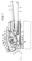
- Fig. 1 is a vertical cross-sectional diagram showing the overall structure of the apparatus, in which indicated by 1 is the main unit of the electrophotographic apparatus.
- a paper guide plate 3 is fitted rotatably on a pivot 2, and a paper tray 4, as an upper body member, is mounted rotatably and detachably on a pivot 4a at the top of the main unit 1.
- the main unit 1 is provided with a paper transportation path 9 for feeding a sheet of paper 7 or 8 in a paper supply cassette 5 or 6, and in the rear of the paper transportation path 9, there is provided a guide plate 10 which confronts the paper guide plate 3 and guides the paper 7 or 8 toward the paper tray 4.
- paper feed rollers 12 and 13 which are in contact with the uppermost ones of papers 7 and 8 in the paper supply cassettes 5 and 6, a transfer device 15 which applies charges to the paper 7 or 8 for transferring a developed image on the photosensitive member 14, a discharging device 16 which removes residual charges on the paper 7 or 8, a fixing device 17 which fixes the transferred image on the paper 7 or 8 that has passed through the transfer device 15, and a separator 11 which is in contact with the fixing roller in the fixing device 17 and function to separate the paper from the fixing roller, all disposed in order from the upperstream to downstream portions of the path.
- the main unit 1 further incorporates a photosensitive member unit 18 and a development device 22, both fitted detachably.
- the photosensitive member unit 18 comprises the photosensitive member 14, a charging device 19 for applying charges to the photosensitive member 14 prior to the formation of a electrostatic latent image, a discharging device 20 which implements the light exposure for the photosensitive member 14 and unifies charges on the exterior surface of the photosensitive member 14, a cleaning device 21, an ozone filter 24, and an exposure device 27 of the self-scanning type, all fitted on the supporting member 18a.
- the supporting member 18a has a formation of a space 18b at the position between the charging device 19 and the ozone filter 24.
- the charging device 19 has a frame 26 with a cross-sectional shape of channel for stretching a charging wire 25.
- the frame 26 is formed by drawing an aluminum bar, and it has a bracket section 28 on its one side surface for supporting the exposure device 27 of the self-scanning type.
- the exposure device 27 is made up of a light emitter 60 fixed to the bracket 28 and a driver 61 which is fixed to the top of the supporting member 18a, both member being connected to each other with a cable.
- the light emitter 60 comprises a light emitting board 29, an end-plane light-emitting board 30 having a linear arrangement of many end-plane light emitting EL elements, although they are not shown in the figure, fixed to the circuit board 29, and a focus lens 32 which is fixed to the bracket 28 by means of a hinge 31 to confront the edge 30a of the end-plane light emitting board 30.
- the driver 61 is a drive circuit board 34, which is connected to the light emitting circuit board 29 by the cable 33, with circuit component parts for driving the end-plane light emitting board 30 and a connector 36 being mounted on the circuit board 34.
- the connector 36 is to make electrical connection from the drive circuit (not shown) fixed in the main unit 1 to the the exposure device 27.
- an insulation board 37 which provides blocking and insulation between the charging device 19 and the exposure device 27 in the vicinity to the photosensitive member 14.
- Indicated by 38 is a cover which is supported by the supporting member 18a and is used to cover the exposure device 27.
- a toner room 50 is formed in the supporting member 18a, and the ozone filter 24 is held on a lid 51 which closes the toner room 50.
- the supporting member 18a has on its both sides formations of shaft holes 42 in which both ends of a shaft 41 for supporting the photosensitive member 14 rotatably are stopped, slits 43 running through the center of the shaft holes 42, and bosses 44 extending outwardly.
- the photosensitive member 14 is fitted to the supporting member 18a by placing both ends of the shaft 41 in the shaft holes 42 while expanding the slits 43 resiliently.
- the photosensitive member unit 18 can be fitted to a frame 45 by inserting the shaft 41 of the photosensitive member 14 into a U-shaped groove 46 of the upper opening formed in the frame 45 which is provided inside the main unit 1 until the bosses 44 are in contact with the upper edge of the frame 45.
- a hook 48 for pushing the shaft 41 to the bottom of the groove 46 is attached rotatably on a pivot 47 on the frame 45. The hook 48 is applied with a force by a toggle spring 49 to both sides of its neutral position.
- the photosensitive member 14 is charged at a certain interval during the rotation by the charging device 19, the charged portion is scanned by the light beam from the exposure device 23, resulting in the formation of an electrostatic latent image, and the image is developed by the development device 22.
- a sheet of paper 7 or 8 in the paper supply cassette 5 or 6 is drawn by the feed roller 12 or 13 to the position between the photosensitive member 14 and transfer device 15, where the developed image on the photosensitive member 14 is transferred to the paper 7 or 8 by the transfer device 15, and, after the image is fixed by the fixing device 17, the paper 7 or 8 is delivered to the paper tray 4.
- the dash-dot line in Fig. 1 when the paper guide plate 3 is swung downward, it functions as the paper tray.
- the paper tray 4 is turned upward around the pivot 4a, the connector 36 is disconnected, the hook 48 is turned so that it retracts from the shaft 41 of the photosensitive member 14, and thereafter the photosensitive member unit 18 is removed to the upward direction, and the paper transportation path 9 is cleared.
- the photosensitive member 14 and exposure device 27 are held by the common supporting member 18a, and hence when the photosensitive member unit 18 is attached to or detached from the main unit 1 for the jam treatment, the relative position between the photosensitive member 14 and exposure device 27 can be retained constant invariably. Since the connector 36 is disposed on the top of the photosensitive member unit 18, it can be connected and disconnected easily, whereby a jam treatment and maintenance activity can be carried out smoothly. In addition, owing to the disposition of the light emitter 60 on the side of the photosensitive member unit 18 and the driver 61 on its top, the exposure device 27 can be made compact.
- the photosensitive member 14 is cleaned by the cleaning device 21, but it may not be cleared of toner completely some times. Although toner is attracted by charges on the photosensitive member 14, a small part of toner may stray from it at portions discharged through the exposure to the light from the exposure device 27. The stray toner will move by being airborne in the turning air stream created by the rotation of the photosensitive member 14, but it does not reach the focus lens 32 by being blocked by the insulation board 37. The insulation board 37 also retards the influence of corona discharge by the charging device 19 on the exposure device 27.
- the turning air stream created by the rotation of the photosensitive member 14 is led together with hot air to the insulation board 37 and they are ventilated effectively through the opening 33.
- the ozone filter 21 is located in this evacuation path, and hence ozone created by the discharging of the charging device 19 can be dissolved effectively by the ozone filter 24.
- the space 18b in front of the ozone filter 24 provides a good route of air stream, and it is also possible to accumulate the ozone stream in this space and conduct it through the ozone filter slowly. Consequently, the ozone stream near the ozone-sourcing charging device 19 can be dissolved promptly.
- the fan can be driven with a small motor, and the noise level of the apparatus can be lowered.
- the ozone filter 24 can easily be replaced.
- corona discharge by the charging device 19 takes place with a negative polarity, and hence toner charged to the negative polarity is attracted to the portions of the photosensitive member 14 which have been discharged through the exposure to the light from the exposure device 27.
- Corona discharge in the transfer device 15 takes place with a positive polarity. Corona discharge with a positive polarity creates little ozone, and therefore no ozone filter is required in the neighborhood of the transfer device 15.
Landscapes
- Physics & Mathematics (AREA)
- General Physics & Mathematics (AREA)
- Engineering & Computer Science (AREA)
- Computer Vision & Pattern Recognition (AREA)
- Electrophotography Configuration And Component (AREA)
- Electrostatic Charge, Transfer And Separation In Electrography (AREA)
- Exposure Or Original Feeding In Electrophotography (AREA)
- Discharging, Photosensitive Material Shape In Electrophotography (AREA)
Claims (4)
- Elektrophotographische Vorrichtung, umfassend:
eine Haupteinheit (1) und ein oberes Gehäuseglied (4), das in der Lage ist, sich bezüglich der Haupteinheit (1) zu öffnen und zu schließen, sodaß ein oberer Bereich der Haupteinheit freigelegt wird;
ein photosensitives Glied (14), das innerhalb der Haupteinheit der Vorrichtung drehbar vorgesehen ist;
eine Ladevorrichtung (19), die so angeordnet ist, daß sie der Außenfläche des photosensitiven Glieds gegenüberliegt, und die dafür eingerichtet ist, das photosensitive Glied zu laden;
eine Belichtungsvorrichtung (27) des Selbstabtast-Typs einschließlich einer linearen Anordnung (60) vieler lichtaussendender Elemente, die auf die Außenfläche des photosensitiven Glieds, das durch die Ladevorrichtung geladen wurde, ein auf einer Bildinformation basierendes Lichtsignal projizieren, um dadurch ein elektrostatisches Latenzbild zu erzeugen;
eine Entwicklungsvorrichtung (22), die so angeordnet ist, daß sie der Außenfläche des photosensitiven Glieds gegenüberliegt, und die dafür eingerichtet ist, das auf dem photosensitiven Glied gebildete, elektrostatische Latenzbild zu entwickeln;
eine Übertragungsvorrichtung (15), die das elektrostatische latente Bild auf dem photosensitiven Glied, das durch die Entwicklungsvorrichtung entwickelt wurde, auf ein Blatt Papier überträgt;
eine Fixiervorrichtung (17), die im Transportpfad des Papiers auf der stromabwärtigen Seite des photosensitiven Glieds angeordnet ist;
gekennzeichnet durch
eine Einheit (18) des photosensitiven Glieds, in der das photosensitive Glied (14), die Belichtungsvorrichtung (27) und ein Verbinder (36) zum Verbinden der Belichtungsvorrichtung mit einer innerhalb der Haupteinheit (1) vorgesehenen Treiberschaltung, angebracht sind, wobei die Einheit (18) des photosensitiven Glieds in der Haupteinheit (1) lösbar angebracht und der Verbinder (36) auf der Oberseite der Einheit (18) des photosensitiven Glieds angeordnet ist, sodaß sie freigelegt werden, wenn das obere Gehäuseglied (4) geöffnet wird, wodurch es ermöglicht wird, den Verbinder (36) und die Einheit (18) des photosensitiven Glieds rasch zu entfernen und einzeln wieder anzubringen, wenn eine Papierstaubehebung oder Wartungsarbeit ausgeführt wird. - Elektrophotographische Vorrichtung nach Anspruch 1, dadurch gekennzeichnet, daß der Treiber (61) der Belichtungsvorrichtung (27), auf dem der Verbinder (36) angebracht ist, auf der Oberseite der Einheit (18) des photosensitiven Glieds angeordnet ist, und auf der Seitenfläche der Einheit (18) des photosensitiven Glieds der Lichtstrahler (60) der Belichtungsvorrichtung (27) derart angeordnet ist, daß der Kopf des Lichtstrahlers (60) dem photosensitiven Glied (14) gegenüberliegt, wobei der Lichtstrahler und der Treiber mit einem Kabel verbunden sind.
- Elektrophotographische Vorrichtung nach einem der vorhergehenden Ansprüche, gekennzeichnet durch ein Sperrglied (37), dessen eine Seite sich in direkter Nähe zum photosensitiven Glied befindet, und das in einer Position zwischen der Ladevorrichtung (19) und der Belichtungsvorrichtung (27) an der Einheit des photosensitiven Glieds angebracht ist.
- Elektrophotographische Vorrichtung nach einem der vorhergehenden Ansprüche, gekennzeichnet durch ein Isolierglied (37), das in einer Position zwischen der Ladevorrichtung (19) und der Belichtungsvorrichtung (27) an der Einheit des photosensitiven Glieds angebracht ist.
Applications Claiming Priority (2)
| Application Number | Priority Date | Filing Date | Title |
|---|---|---|---|
| JP2020904A JPH03225371A (ja) | 1990-01-31 | 1990-01-31 | 電子写真装置 |
| JP20904/90 | 1990-01-31 |
Publications (3)
| Publication Number | Publication Date |
|---|---|
| EP0440407A2 EP0440407A2 (de) | 1991-08-07 |
| EP0440407A3 EP0440407A3 (en) | 1992-05-20 |
| EP0440407B1 true EP0440407B1 (de) | 1995-06-07 |
Family
ID=12040220
Family Applications (1)
| Application Number | Title | Priority Date | Filing Date |
|---|---|---|---|
| EP91300644A Expired - Lifetime EP0440407B1 (de) | 1990-01-31 | 1991-01-29 | Elektrophotographisches Gerät |
Country Status (5)
| Country | Link |
|---|---|
| US (1) | US5155506A (de) |
| EP (1) | EP0440407B1 (de) |
| JP (1) | JPH03225371A (de) |
| KR (1) | KR940005126B1 (de) |
| DE (1) | DE69110146T2 (de) |
Families Citing this family (9)
| Publication number | Priority date | Publication date | Assignee | Title |
|---|---|---|---|---|
| JPH03225375A (ja) * | 1990-01-31 | 1991-10-04 | Tokyo Electric Co Ltd | 電子写真装置 |
| US5640548A (en) * | 1992-10-19 | 1997-06-17 | Motorola, Inc. | Method and apparatus for unstacking registers in a data processing system |
| US5390011A (en) * | 1993-05-27 | 1995-02-14 | Delphax Systems | Compact imaging roll printer |
| JP3332818B2 (ja) * | 1996-08-29 | 2002-10-07 | キヤノン株式会社 | プロセスカートリッジ及び電子写真画像形成装置及び接続端子の接続方法 |
| DE19854991B4 (de) * | 1997-12-04 | 2005-11-10 | Ricoh Co., Ltd. | Bilderzeugungsapparat und Verfahren zum Zusammenbauen desselben |
| US6201556B1 (en) * | 1999-11-19 | 2001-03-13 | Nexpress Solutions Llc | Electrographic reproduction apparatus light-emitting device support mechanism |
| US6263177B1 (en) | 2000-05-19 | 2001-07-17 | Nexpress Solutions Llc | Document printer/copier with decoupleable drum-support member |
| DE10122237A1 (de) * | 2000-05-17 | 2001-12-20 | Heidelberger Druckmasch Ag | Elektrostatische Bildentwicklungsvorrichtung |
| US6396524B1 (en) * | 2000-05-18 | 2002-05-28 | Nexpress Solutions Llc | Skew adjustment for optical writer in a document printer/copier |
Family Cites Families (18)
| Publication number | Priority date | Publication date | Assignee | Title |
|---|---|---|---|---|
| JPS5778075A (en) * | 1980-10-31 | 1982-05-15 | Toshiba Corp | Photoreceptor holding device for picture forming equipment |
| JPS58192059A (ja) * | 1982-05-06 | 1983-11-09 | Canon Inc | 画像形成装置 |
| JPS59123860U (ja) * | 1983-02-09 | 1984-08-21 | キヤノン株式会社 | 画像形成装置 |
| US4535341A (en) * | 1983-08-19 | 1985-08-13 | Westinghouse Electric Corp. | Thin film electroluminescent line array emitter and printer |
| JPS60205462A (ja) * | 1984-03-29 | 1985-10-17 | Kyocera Corp | 画像形成装置 |
| JPS6156370A (ja) * | 1984-08-28 | 1986-03-22 | Ricoh Co Ltd | 画像形成装置 |
| JPH0665497B2 (ja) * | 1984-12-28 | 1994-08-24 | オリンパス光学工業株式会社 | 画像形成装置 |
| US4785319A (en) * | 1986-08-05 | 1988-11-15 | Canon Kabushiki Kaisha | Electrographic apparatus |
| JPS6395464A (ja) * | 1986-10-09 | 1988-04-26 | Sharp Corp | 複写機 |
| JP2539803B2 (ja) * | 1986-12-22 | 1996-10-02 | 株式会社東芝 | 記録装置 |
| JPS63210857A (ja) * | 1987-02-27 | 1988-09-01 | Nec Corp | プロセスキツト |
| US4796037A (en) * | 1987-03-11 | 1989-01-03 | Ricoh Company, Limited | Compact image recording apparatus having an up-side down structure |
| JPH0682245B2 (ja) * | 1987-12-22 | 1994-10-19 | キヤノン株式会社 | 画像形成装置 |
| CA1327831C (en) * | 1988-05-25 | 1994-03-15 | Shigeki Sakakura | Image-forming apparatus |
| JPH0782288B2 (ja) * | 1988-06-03 | 1995-09-06 | 富士通株式会社 | プロセスカートリッジ及びそれを使用した画像形成装置 |
| JP2788285B2 (ja) * | 1988-09-12 | 1998-08-20 | 株式会社リコー | 画像記録装置 |
| JPH02158764A (ja) * | 1988-12-13 | 1990-06-19 | Sharp Corp | プロセスカートリッジ |
| JP2568740B2 (ja) * | 1990-08-13 | 1997-01-08 | 三菱電機株式会社 | 電子写真装置 |
-
1990
- 1990-01-31 JP JP2020904A patent/JPH03225371A/ja active Pending
-
1991
- 1991-01-14 KR KR1019910000442A patent/KR940005126B1/ko not_active Expired - Fee Related
- 1991-01-29 EP EP91300644A patent/EP0440407B1/de not_active Expired - Lifetime
- 1991-01-29 DE DE69110146T patent/DE69110146T2/de not_active Expired - Fee Related
- 1991-01-31 US US07/648,230 patent/US5155506A/en not_active Expired - Fee Related
Also Published As
| Publication number | Publication date |
|---|---|
| JPH03225371A (ja) | 1991-10-04 |
| KR940005126B1 (ko) | 1994-06-11 |
| US5155506A (en) | 1992-10-13 |
| EP0440407A2 (de) | 1991-08-07 |
| DE69110146D1 (de) | 1995-07-13 |
| EP0440407A3 (en) | 1992-05-20 |
| KR910014772A (ko) | 1991-08-31 |
| DE69110146T2 (de) | 1996-02-01 |
Similar Documents
| Publication | Publication Date | Title |
|---|---|---|
| US8014696B2 (en) | Image forming device | |
| CN100501579C (zh) | 成像装置 | |
| US7146120B2 (en) | Image forming apparatus having a corona discharge air supplying section | |
| JPH05216305A (ja) | 画像形成装置 | |
| EP0440407B1 (de) | Elektrophotographisches Gerät | |
| US7555235B2 (en) | Image forming apparatus enabling user to directly clean discharge wire | |
| US20050089315A1 (en) | Optical writing device and image forming apparatus including the optical writing device that prevents scattered toner and powder dust from entering the optical writing device | |
| JP3315596B2 (ja) | 画像形成装置 | |
| EP0440404B1 (de) | Elektrofotografisches Gerät | |
| JPH03213887A (ja) | 電子写真装置の転写装置 | |
| US5426496A (en) | Printing apparatus | |
| JP2002196635A (ja) | 帯電装置、及び画像形成装置 | |
| JP2004333799A (ja) | 画像形成装置 | |
| GB2228446A (en) | Image forming apparatus | |
| US4774531A (en) | Recording apparatus | |
| US10969732B2 (en) | Image forming apparatus including optical print head | |
| JP3288075B2 (ja) | 静電潜像の記録装置 | |
| JP3587566B2 (ja) | カラー電子写真装置 | |
| JPH0618366Y2 (ja) | 画像形成装置 | |
| JPH05323698A (ja) | 作像装置 | |
| JP2858545B2 (ja) | 画像記録装置 | |
| JP2614032B2 (ja) | 画像記録装置 | |
| JP3135556B2 (ja) | 電子写真装置 | |
| JPH03225372A (ja) | 電子写真装置 | |
| JP3091559B2 (ja) | 画像形成装置 |
Legal Events
| Date | Code | Title | Description |
|---|---|---|---|
| PUAI | Public reference made under article 153(3) epc to a published international application that has entered the european phase |
Free format text: ORIGINAL CODE: 0009012 |
|
| 17P | Request for examination filed |
Effective date: 19910205 |
|
| AK | Designated contracting states |
Kind code of ref document: A2 Designated state(s): DE FR GB |
|
| PUAL | Search report despatched |
Free format text: ORIGINAL CODE: 0009013 |
|
| AK | Designated contracting states |
Kind code of ref document: A3 Designated state(s): DE FR GB |
|
| 17Q | First examination report despatched |
Effective date: 19931005 |
|
| GRAA | (expected) grant |
Free format text: ORIGINAL CODE: 0009210 |
|
| AK | Designated contracting states |
Kind code of ref document: B1 Designated state(s): DE FR GB |
|
| PG25 | Lapsed in a contracting state [announced via postgrant information from national office to epo] |
Ref country code: FR Effective date: 19950607 |
|
| REF | Corresponds to: |
Ref document number: 69110146 Country of ref document: DE Date of ref document: 19950713 |
|
| EN | Fr: translation not filed | ||
| RAP2 | Party data changed (patent owner data changed or rights of a patent transferred) |
Owner name: KABUSHIKI KAISHA TEC |
|
| PGFP | Annual fee paid to national office [announced via postgrant information from national office to epo] |
Ref country code: GB Payment date: 19960122 Year of fee payment: 6 |
|
| PGFP | Annual fee paid to national office [announced via postgrant information from national office to epo] |
Ref country code: DE Payment date: 19960126 Year of fee payment: 6 |
|
| PLBE | No opposition filed within time limit |
Free format text: ORIGINAL CODE: 0009261 |
|
| STAA | Information on the status of an ep patent application or granted ep patent |
Free format text: STATUS: NO OPPOSITION FILED WITHIN TIME LIMIT |
|
| 26N | No opposition filed | ||
| PG25 | Lapsed in a contracting state [announced via postgrant information from national office to epo] |
Ref country code: GB Effective date: 19970129 |
|
| GBPC | Gb: european patent ceased through non-payment of renewal fee |
Effective date: 19970129 |
|
| PG25 | Lapsed in a contracting state [announced via postgrant information from national office to epo] |
Ref country code: DE Effective date: 19971001 |